Theoretical and experimental discovery of single-Dirac-cone topological-insulator class was reported in the same paper at arXiv:0812.2078 (2008) [http://arxiv.org/abs/0812.2078]. Perspectives and Published version at Y. Xia et.al., Nature Physics 5, 398-402 (2009) [http://dx.doi.org/10.1038/nphys1294].
First observation of Spin-Momentum helical locking in Bi2Se3 and Bi2Te3, demonstration of Topological-Order at 300K and a realization of topological-transport-regime
Helical Dirac fermions - charge carriers that behave as massless relativistic particles with a quantum magnetic moment that is locked to its direction of motion - are proposed to be the key to realizing fundamentally new phenomena in condensed matter physics 1 ; 2 . Prominent examples include the anomalous quantization of magneto-electric coupling 3 ; 4 ; 5 ; 6 , half-fermion states that are their own anti-particle 7 ; 8 , and charge fractionalization in a Bose-Einstein condensate 9 , all of which are not possible with conventional Dirac fermions of the graphene variety 10 . Helical Dirac fermions are challenging to find, and so far remain undiscovered, because they are forbidden to exist in ordinary Dirac materials such as graphene 10 or bismuth 11 , and because the necessary spin-sensitive measurements are lacking. It has recently been proposed that helical Dirac fermions may exist at the edges of certain types of topologically ordered insulators 3 ; 4 ; 12 , and that their peculiar properties may be accessed provided the insulator is tuned into a topological transport regime 3 ; 4 ; 5 ; 6 ; 7 ; 8 ; 9 . However, helical Dirac fermions have not been observed in existing topological insulators 13 ; 14 ; 15 ; 16 ; 17 ; 18 to date because conventional electrical gating based tuning techniques that work for graphene 10 ; 19 cannot be applied and the necessary spin-resolved photoelectron detections do not exist. Here we report the first realization of a tunable topological insulator in a bismuth based class by combining spin- and momentum-resolved spectroscopies, bulk charge compensation and surface control. Our results reveal a spin-momentum locked Dirac cone that is nearly 100% spin-polarized, which exhibits a tunable topological fermion density in the vicinity of the Kramers’ point and can be driven to the long-sought topological transport regime. The observed topological nodal Dirac ground state is found to be protected even up to room temperature (300 K). Our results on Bi2-δCaδSe3.NO2 pave the way for future transport based studies of topological insulators, and possible room temperature applications of protected spin-polarized edge channels in microelectronics technology.
Unlike conventional Dirac fermions as in graphene, helical Dirac fermions possess a net spin and are guaranteed to be conducting because of time-reversal symmetry 3 ; 4 ; 5 , allowing the unique possibility to carry spin currents without heat dissipation. However, the most important difference lies in the topological properties of helical Dirac fermion systems 3 ; 4 ; 5 ; 12 , which are predicted to manifest in several ways, provided the system can be tuned to the topological transport regime where the charge density vanishes (analogous to the charge neutrality point in graphene 19 ). These manifestations include an anomalous half-integer quantization of Hall conductance 3 ; 4 ; 5 ; 6 , a realization of Majorana fermions (particles with anyon exchange statistics that differs from the conventional Bose or Fermi-Dirac statistics) 7 ; 8 , and a generation of fractionally charged particles 9 . Helical fermions are believed to exist on the edges of certain types of three-dimensional (3D) topological insulators 3 ; 4 ; 12 , with material candidates Bi2X3 (X = Se, Te) recently proposed based on observations 15 ; 17 and models 4 ; 20 . However, these materials cannot be used to detect helical Dirac fermion physics for three reasons: First, the helical properties of the surface electrons are unknown and depend on the materials class. Second, their electronic structure is not in the topological transport regime, thus not allowing any of the interesting topological insulator experiments to be performed to this date. And third, unlike 2D quantum Hall Dirac systems such as graphene 10 ; 19 , 3D topological insulators cannot be tuned to this zero carrier density regime through electrical gating, which has prevented a revolution like that witnessed for graphene 10 from taking place for topological insulators.
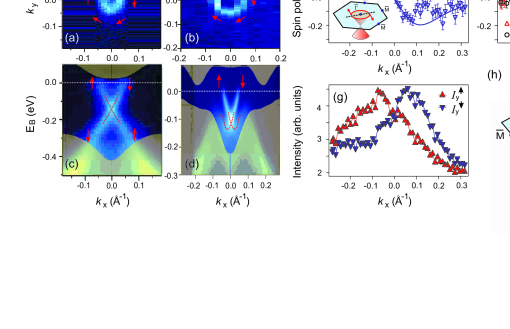
To determine the key helical properties of the surface electrons near the Fermi level () in the candidate Bi2X3 class, we performed spin- and angle-resolved photoemission spectroscopy (ARPES) scans using a double Mott detector setup 21 , which systematically measures all three components of the spin of a photoelectron as a function of its energy and momentum throughout the Brillouin zone (Supplementary Information). Although the surface electrons of both Bi2Se3 and Bi2Te3 exhibit a finite density of states near (Figs 1(a)-(d)), there is an additional contribution to the density of states around momentum from the spin-degenerate bulk conduction band in Bi2Se3 15 . Therefore, the helical nature of the surface electrons is most clearly resolved in Bi2Te3. We analyzed the spin-polarization of photoelectrons emitted at a binding energy = -20 meV along the ( -M̄) cut in Bi2Te3 (inset Fig. 1(e)). Because the surface state dispersion of Bi2X3 exhibits a pronounced time dependence after cleavage (SI) related to semiconductor band bending effects 17 , data collection times were only long enough to ensure a level of statistics sufficient to measure the spin-polarized character of the surface states.
Figures 1(e) and (f) show the measured spin polarization spectra of the = , and (out-of-plane) components along the -M̄ direction. In the and directions, no clear signal can be discerned within the margins of statistical error. In the direction on the other hand, clear polarization signals of equal magnitude and opposite sign are observed for surface electrons of opposite momentum, evidence that the spin and momentum directions are one-to-one locked. This is most clearly seen in the spin-resolved spectra (; Fig. 1(g)), which are calculated from according to = (1+)/2 and = (1-)/2, where is the spin-averaged intensity. To extract the spin polarization vectors of the forward (+) and backward (-) moving electrons, we performed a standard numerical fit (SI) 21 . The fit results yield 100(15)% polarized (see Fig. 1(h)) spins that point along the (kz) direction, which is consistent with its spin-orbit coupling origin 14 ; 21 . Our combined observations of a linear dispersion relation and a one-to-one locking of momentum and spin directions allow us to conclude that the surface electrons of Bi2X3 (X = Se, Te) are helical Dirac fermions of topological order origin (Fig. 1).

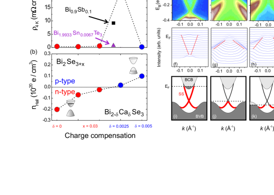
To experimentally access these helical Dirac fermions for research device applications, the electronic structure must be in the topological transport regime where there is zero charge fermion density 7 ; 8 ; 9 . This regime occurs when lies in between the bulk valence band maximum (VBM) and the bulk conduction band minimum (CBM), and exactly at the surface Dirac point, which should in turn lie at a Kramers’ time-reversal invariant momentum 3 ; 4 . This is clearly not the case in either Bi2Te3, Bi2(Sn)Te3, Bi2Se3 or graphene. Although pure Bi2X3 are expected to be undoped semiconductors 20 ; 22 ; 23 , nominally stoichiometric samples are well known to be n- and p-type semiconductors due to excess carriers introduced via Se or Te site defects respectively 16 ; 17 . To compensate for the unwanted defect dopants, trace amounts of carriers of the opposite sign must be added into the naturally occurring material, which may be easier to achieve in Bi2Se3 than in Bi2Te3 because it has a larger band gap 24 (around 0.35 eV 25 compared to 0.18 eV 26 respectively). To lower the of Bi2Se3 into the bulk band gap, we substituted trace amounts of Ca2+ for Bi3+ in as-grown Bi2Se3, where Ca has been shown to act as a hole donor by scanning tunnelling microscopy and thermoelectric transport studies 16 . Figure 2(a) shows that as the Ca concentration increases from 0% to 0.5%, the low temperature resistivity sharply peaks at 0.25%, which suggests that the system undergoes a metal to insulator to metal transition. The resistivity peak occurs at a Ca concentration where a change in sign of the Hall carrier density also is observed (Fig. 2(b)), which shows that for measured Ca concentrations below and above 0.25%, electrical conduction is supported by electron and hole carriers respectively.

We performed systematic time-dependent ARPES measurements to study the electronic structure evolution of Bi2-δCaδSe3 as a function of Ca doping in order to gain insight into the trends observed in transport (Figs 2(a) and (b)). Early time ARPES energy dispersion maps taken through the point of the (111) surface Brillouin zone are displayed in Figure 2(c)-(h) for several Ca doping levels. In the as-grown ( = 0) Bi2Se3 samples, a single surface Dirac cone is observed with lying nearly 0.3 eV above the Dirac node forming an electron Fermi surface (FS). We also observe that intersects the electron-like bulk conduction band. When a 0.25% concentration of Ca is introduced, is dramatically lowered to lie near the Dirac node (Fig. 2(d)), which is consistent with Ca acting as a highly effective hole donor. Because the bulk CBM lies at a binding energy of approximately -0.1 eV for = 0 (Fig. 2(c)), an 0.3 eV shift in between = 0 and = 0.0025 suggests that for = 0.0025, is located 0.2 eV below the CBM. This is consistent with being in the bulk band gap because the indirect energy gap between the CBM and the VBM is known from both tunneling 24 and optical 25 data and theory 22 to be nearly 0.35 eV.
As the Ca concentration is increased further, the position of continues a downward trend such that by = 0.01, it is located clearly below the Dirac node (Fig. 2(e)) and intersects the hole-like bulk valence band. The systematic lowering of with increasing in Bi2-δCaδSe3 observed in early time ARPES measurements (Figs 2(i)-(k)), which reflect the electronic structure of the sample bulk, consistently explain the measured transport behavior. However, we observe that rises back up over time across all samples such that all spectra relax back to a = 0 like spectrum on a typical time scale of 18 hours (Fig. 2(l)). Such a slow upward shift of the surface Fermi level has been observed also in Bi2Te3 17 and is due to a surface band bending effect commonly observed in most semiconductors (SI). Therefore, although bulk Ca doping succeeds in tuning between the bulk valence and conduction bands, it does not change the position of relative to the surface Dirac point in the ground state.
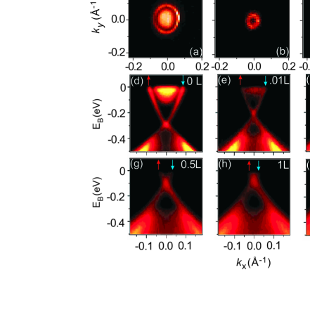
Because the surface Dirac point in the ground state of most insulating Bi1.9975Ca0.0025Se3 lies 0.3 eV below , its electronic structure is still not in the much desired topological transport regime. To bring the surface Dirac point level with in Bi2-δCaδSe3, we show that hole carriers can be systematically introduced into the surface by dosing with NO2 molecules, which has been demonstrated in graphene 27 ; 28 . Figure 3 shows that with increasing surface hole donor concentration, the binding energy of the surface Dirac point rises monotonically towards . Starting from -0.3 eV at a 0 Langmuir (L) dose, it rises to -0.15 eV at 0.1 L where the surface bent CBM has completely disappeared, and finally to the charge neutrality point ( = 0 eV) at 2 L. No further changes of the chemical potential are observed with higher dosages. To quantify the surface carrier density () dependence on surface hole donor concentration, we mapped the surface state FS in Figures 3(a)-(c) and performed an electron count based on FS area = /, where is the area of the FS and is the area of the surface Brillouin zone. We find that 0.1 L of NO2 removes approximately 0.0066 electrons per surface unit cell of Bi2-δCaδSe3 (111), and an excess of 2 L reduces the FS to a single point within our experimental resolution, which has an additional 0.005 electrons per unit cell removed. Because surface doping does not affect the carrier density in the bulk (which thus remains insulating), the energy of the Dirac point is lifted above the bulk VBM; a new time independent electronic ground state is realized that lies in the topological transport regime with intersecting the Dirac node.
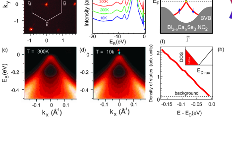
In order to investigate the thermal stability of this nodal Dirac ground state (Fig. 4(e)), temperature dependent ARPES scans were collected on Bi2-δCaδSe3 samples that were first surface hole doped with NO2 at a temperature = 10 K. Figures 4(c) and (d) illustrate that the charge neutral point-like FS (Fig. 4(a)) is robust up to room temperature ( = 300 K) over days long measurement times. A density of states that decreases linearly to zero at the Dirac point energy at 300 K (Fig. 4(f)) is further evidence that the low energy properties of Bi1.9975Ca0.0025Se3.NO2 are dominated by a novel ground state that features massless helical Dirac fermions with nearly 100% spin polarization. This also confirms a non-trivial Berry s phase on the surface due to the spin-momentum locking pattern that we observe, which is similar to the robust Berry s phase previously observed in the Bi-Sb system 14 (Fig. 1).
Helical nodal Dirac fermions are forbidden from acquiring a mass through band gap formation because they are located around time-reversal invariant (Kramers’) momenta = or M̄ (Fig. 4(h)). This makes them fundamentally different from chiral Dirac fermions such as those found in graphene, which are located at K̄ and not topologically protected (Fig. 4(g)). The helical Dirac fermion on the surface of Bi2Se3 owes its existence to a non-zero topological number given by (-1) = (), where () is the parity eigenvalue of the bulk wavefunction at the 3D Kramers’ point and is the number of occupied bulk bands 4 . Because Ca dopants are present in only trace quantities in Bi1.9975Ca0.0025Se3.NO2, the values of () do not deviate from those of pure Bi2Se3, as evidenced by the persistence of a single gapless surface band in both Bi2Se3 and Bi1.9975Ca0.0025Se3. Both Ca2+ and NO2- are non-magnetic and so do not break time-reversal symmetry, therefore the same topological number ( = 1) applies even in the Dirac transport regime (Fig. 4) realized by our method shown here, which is stable with both time and temperature. Our direct demonstration of spin-polarized edge channels and room temperature operability of chemically gated stoichiometric Bi2Se3 or Bi2-δCaδSe3, not achieved in purely 2D topological systems such as Hg(Cd)Te quantum wells 29 , enables exciting future room temperature experiments on surface helical Dirac fermions that carry a non-trivial Berry’s phase.

Our demonstration of topological order at room temperature opens up possibilities of using quantum Hall-like phenomena and spin-polarized protected edge channels for spintronic or computing device applications without the traditional requirements of high magnetic fields and delicate cryogenics. A direct detection of surface-edge states would be possible in stoichiometric Bi2Se3 or Bi2-δCaδSe3, using transport methods which will bear signatures of weak anti-localization and thus exhibit anomalous magneto-optic effects. Here we envisage a few sample experiments that could be carried out by using surface doped or electrically gated Bi2-δCaδSe3. By applying a weak time-reversal breaking perturbation at the surface of Bi2-δCaδSe3.NO2 so as to lift the Kramers’ degeneracy at (A method of gap opening on the surface is shown in the SI), a half-integer quantized magneto-electric coupling can be realized 3 ; 4 ; 5 ; 6 , which may be measured by standard Hall probes. This would enable a variety of novel surface quantum Hall physics to be realized. Another class of experiments would be made possible by interfacing the helical topological surface with magnetic and ordinary superconducting films. An interferometer device can be built based on Bi2-δCaδSe3 that is used to create and detect long-sought Majorana fermions 7 ; 8 . These particles, which have never been experimentally observed, possess only half the degrees of freedom of a conventional fermion and constitute the key building block for topological quantum computing that can operate in fault-tolerant mode. Yet another class of experiments would be made possible by sandwiching a charge neutral topological insulator film made of Bi2-δCaδSe3 within a charged capacitor. In this way, a microchip that supports a topological electron-hole condensate with fractionally charged vortices 9 can be fabricated, which offers the exciting opportunity to probe interactions between Dirac fermions of opposite helicity; this would enable searching for exotic quantum phenomena beyond the standard model of particle physics 30 .
Acknowledgements The spin-resolved ARPES measurements are supported by NSF through the Center for Complex Materials (DMR-0819860) and Princeton University; the use of synchrotron X-ray facilities (ALS-LBNL Berkeley) is supported by the Basic Energy Sciences of the U.S. Department of Energy (DE-FG-02-05ER46200) and by the Swiss Light Source, Paul Scherrer Institute, Villigen, Switzerland.
Author information Correspondence and requests for materials should be addressed to M.Z.H (mzhasan@princeton.edu).
I Methods
Spin-integrated ARPES data were taken at beamlines 12.0.1 and 7.0.1 of the Advanced Light Source in Lawrence Berkeley National Laboratory with 29 eV to 100 eV photons. Typical energy and momentum resolutions were 15 meV and 1% of the surface BZ and 50 meV and 2% of the surface BZ respectively. Spin-resolved ARPES measurements were performed at the SIS beamline at the Swiss Light Source using the COPHEE spectrometer, which consists of two 40 kV classical Mott detectors that measure all three spatial components of spin polarization. Spin-resolved measurements were taken with 20 eV to 22 eV photons with energy and momentum resolutions of 80 meV and 3% of the surface BZ respectively. Spin-integrated data were collected on Bi2-δCaδSe3 and Bi2Te3 single crystals cleaved in ultra high vacuum pressures better than torr and maintained at a temperature of 10 K unless otherwise specified. Spin-resolved data were collected at 50 K. Adsorption of NO2 molecules on Bi2-δCaδSe3 was achieved via controlled exposures to NO2 gas (Matheson, 99.5%). The adsorption effects were studied under static flow mode by exposing the cleaved sample surface to the gas for a certain time then taking data after the chamber was pumped down to the base pressure. Spectra of the NO2 adsorbed surfaces were taken within minutes of opening the photon shutter to minimize photon exposure related effects. The calculations were performed with the LAPW method in slab geometry using the WIEN2K package.
References
- (1) Day, C. Exotic spin textures show up in diverse materials. Phys. Today 62, 12-13 (2009). http://dx.doi.org/10.1063/1.3120883
- (2) Moore, J. E. Topological insulators: The next generation. Nature Phys. 5, 378-380 (2009). http://dx.doi.org/10.1038/nphys1294
- (3) Fu, L., Kane, C. L. & Mele, E. J. Topological insulators in three dimensions. Phys. Rev. Lett. 98, 106803 (2007).
- (4) Fu, L. & Kane, C. L. Topological insulators with inversion symmetry. Phys. Rev. B. 76, 045302 (2007).
- (5) Qi, X.-L., Hughes, T. L. & Zhang, S.-C. Topological field theory of time-reversal invariant insulators. Phys. Rev. B 78, 195424 (2008).
- (6) Essin, A., Moore, J. E. & Vanderbilt, D. Magnetoelectric polarizability and axion electrodynamics in crystalline insulators. Phys. Rev. Lett. 102, 146805 (2009).
- (7) Fu, L. & Kane, C. L. Probing neutral Majorana fermion edge modes with charge transport. Phys. Rev. Lett. 102, 216403 (2009).
- (8) Akhmerov, A. R., Nilsson, J. & Beenakker, C. W. J. Electrically detected interferometry of Majorana fermions in a topological insulator. Phys. Rev. Lett. 102, 216404 (2009).
- (9) Seradjeh, B., Moore, J. E. & Franz, M. Exciton condensation and charge fractionalization in a topological insulator film. Phys. Rev. Lett. 103, 066402 (2009).
- (10) Geim, A. K. & Novoselov, K. S. The rise of graphene. Nature Mat. 6, 183-191 (2007).
- (11) Li, L. et al. Phase transitions of Dirac electrons in Bismuth. Science 321, 547-550 (2008).
- (12) Moore, J. E. & Balents, L. Topological invariants of time-reversal-invariant band structures. Phys. Rev. B 75 121306(R) (2007).
- (13) Hsieh, D. et al. A topological Dirac insulator in a quantum spin Hall phase. Nature 452, 970-974 (2008).
- (14) Hsieh, D. et al. Observation of unconventional quantum spin textures in topological insulators. Science 323, 919-922 (2009).
- (15) Xia, Y. et al. Observation of a large-gap topological-insulator class with a single Dirac cone on the surface. Nature Phys. 5, 398-402 (2009).
- (16) Hor, Y. S. et al. p-type Bi2Se3 for topological insulator and low-temperature thermoelectric applications. Phys. Rev. B 79, 195208 (2009).
- (17) Noh, H.-J. et al. Spin-orbit interaction effect in the electronic structure of Bi2Te3 observed by angle-resolved photoemission spectroscopy. Europhys. Lett. 81, 57006 (2008).
- (18) Nishide, A. et al. Direct mapping of the spin-filtered surface bands of a three-dimensional quantum spin Hall insulator. Preprint at ¡http://arxiv.org/abs/0902.2251¿ (2009).
- (19) Checkelsky, J. G., Li, L. & Ong, N. P. Divergent resistance of the Dirac point in graphene: Evidence for a transition in high magnetic field. Phys. Rev. B 79, 115434 (2009).
- (20) Zhang, H. et al. Topological insulators in Bi2Se3, Bi2Te3 and Sb2Te3 with a single Dirac cone on the surface. Nature Phys. 5, 438-442 (2009).
- (21) Meier, F., Dil, J. H., Lobo-Checa, J., Patthey, L. & Osterwalder, J. Quantitative vectorial spin analysis in angle-resolved photoemission: Bi/Ag(111) and Pb/Ag(111). Phys. Rev. B 77, 165431 (2008).
- (22) Larson, P. et al. Electronic structure of Bi2X3 (X = S, Se, T) compounds: Comparison of theoretical calculations with photoemission studies. Phys. Rev. B 65, 085108 (2001).
- (23) Mishra, S. K., Satpathy, S. & Jepsen, O. Electronic structure and thermoelectric properties of bismuth telluride and bismuth selenide. J. Phys: Condens. Mat. 9, 461-470 (1997).
- (24) Urazhdin, S. et al. Surface effects in layered semiconductors Bi2Se3 and Bi2Te3. Phys. Rev. B 69, 085313 (2004).
- (25) Black, J., Conwell, E. M., Seigle, L. & Spencer, C. W. Electrical and optical properties of some MN semiconductors. J. Phys. Chem. Sol. 2, 240-251 (1957).
- (26) Thomas, G. A. et al. Large electron-density increase on cooling a layered metal: Doped Bi2Te3. Phys. Rev. B 46, 1553-1556 (1992).
- (27) Zhou, S. et al. A. Metal to insulator transition in epitaxial graphene induced by molecular doping. Phys. Rev. Lett. 101, 086402 (2008).
- (28) Schedin, F. et al. Detection of individual gas molecules adsorbed on graphene. Nature Mat. 6, 652-655 (2007).
- (29) Konig, M. et al. Quantum spin Hall insulator state in HgTe quantum wells. Science 318, 766-770 (2007).
- (30) Wilczek, F. Remarks on dyons. Phys. Rev. Lett. 48, 1146-1149 (1982).
Figure 1 : Detection of spin-momentum locking of spin-helical Dirac electrons in Bi2Se3 and Bi2Te3 using spin-resolved ARPES. (a) ARPES intensity map at of the (111) surface of tuned Bi2-δCaδSe3 (see text) and (b) the (111) surface of Bi2Te3. Red arrows denote the direction of spin around the Fermi surface. (c) ARPES dispersion of tuned Bi2-δCaδSe3 and (d) Bi2Te3 along the cut. The dotted red lines are guides to the eye. The shaded regions in (c) and (d) are our calculated projections of the bulk bands of pure Bi2Se3 and Bi2Te3 onto the (111) surface respectively. (e) Measured component of spin-polarization along the -M̄ direction at = -20 meV, which only cuts through the surface states. Inset shows a schematic of the cut direction. (f) Measured (red triangles) and (black circles) components of spin-polarization along the -M̄ direction at = -20 meV. Error bars in (e) and (f) denote the standard deviation of , where typical detector counts reach ; Solid lines are numerical fits 21 . (g) Spin-resolved spectra obtained from the component spin polarization data. The non-Lorentzian lineshape of the and curves and their non-exact merger at large is due to the time evolution of the surface band dispersion, which is the dominant source of statistical uncertainty. a.u., arbitrary units. (h) Fitted values of the spin polarization vector P = (,,) are (sin(90∘)cos(-95∘), sin(90∘)sin(-95∘), cos(90∘)) for electrons with + and (sin(86∘)cos(85∘), sin(86∘)sin(85∘), cos(86∘)) for electrons with -, which demonstrates the topological helicity of the spin-Dirac cone. The angular uncertainties are of order 10∘ and the magnitude uncertainty is of order 0.15.
Figure 2 : Tuning the bulk Fermi level through systematic bulk charge compensation monitored through systematic transport and ARPES measurements. (a) Resistivity at T = 4 K measured for samples of Bi2Se3 that are bulk electron doped due to varying concentrations of Se vacancies 16 () or bulk hole doped through Ca/Bi substitution (). These are compared to analogous values for topological insulators Bi0.9Sb0.1 (black square, arrowed; 13 ) and Bi1.9933Sn0.0067Te3 (purple triangle, arrowed). The stoichiometric Bi2Se3 (Bi1.9975Ca0.0025Se3) is found to be the most insulating of these topological insulators. In Bi2-δCaδSe3, bulk resistivity in excess of 75 mcm is possible, which will be shown elsewhere. The bulk insulating state in Bi0.9Sb0.1 13 is intrinsic and not due to disorder which will also be shown elsewhere. Bi1.9975Ca0.0025Se3 is known to be most metallic-like among the three classes studied so far. (b) Hall carrier density of the same samples determined using Hall measurements. Symbols colored red (blue) represent n- (p-) type behavior. (c) ARPES band dispersion images of Bi2-δCaδSe3 (111) through collected within 20 minutes after cleavage for = 0, (d) = 0.0025 and (e) = 0.01. Panels (f) through (h) show the corresponding momentum distributions curves. Red lines are guides to the eye. Panels (i) through (k) show the schematic downward evolution of with increasing Ca content. The occupied bulk conduction band (BCB) and bulk valence band (BVB) states are shaded dark, and the occupied surface states (SS) are colored red. (l) Typical ARPES band dispersion image of panels (c) through (e) taken around 18 hours after cleavage and (m) its corresponding momentum distribution curves. (n) Schematic of the surface band bending process that is responsible for the observed downward shift in energies over time. Vac., vacuum.
Figure 3: Tuning the density of helical Dirac electrons to the spin-degenerate Kramers point and topological transport regime. (a) A high resolution ARPES mapping of the surface Fermi surface (FS) near of Bi2-δCaδSe3 (111). The diffuse intensity within the ring originates from the bulk-surface resonance state 15 . (b) The FS after 0.1 Langmuir (L) of NO2 is dosed, showing that the resonance state is removed. (c) The FS after a 2 L dosage, which achieves the Dirac charge neutrality point. (d) High resolution ARPES surface band dispersions through after an NO2 dosage of 0 L, (e) 0.01 L, (f) 0.1 L, (g) 0.5 L, (h) 1 L and (i) 2 L. The arrows denote the spin polarization of the bands. We note that due to an increasing level of surface disorder with NO2 adsorption, the measured spectra become progressively more diffuse and the total photoemission intensity from the buried Bi2-δCaδSe3 surface is gradually reduced.
Figure 4 : Topological order of the nodal helical Dirac ground state at 300 K. (a) Typical ARPES intensity map of the Bi2(Se/Te)3 class collected at spanning several Brillouin zones. (b) Energy distribution curves of the valence bands of Bi2-δCaδSe3 taken at T = 10 K, 200 K and 300 K. The peaks around -4 eV and -7.5 eV come from NO2 adsorption (SI). The intensity of these NO2 core level peaks do not change over this temperature range, indicating no measurable NO2 desorption during the heating process. (c) ARPES intensity map of the surface state band dispersion of Bi2-δCaδSe3 (111) after a 2 L dosage of NO2 is applied at T = 10 K, which is taken at 300 K and (d) 10 K. (e) Schematic of the surface and bulk electronic structure of Bi2-δCaδSe3.NO2, tuned to the topological transport regime. (f) Angle-integrated intensity near (red) shows a linear trend. The inset shows the expected density of states (DOS) of a helical Dirac cone, which is 1/2 that of a graphene Dirac cone due to its single spin degeneracy. (g) Schematic of the chiral Dirac fermion ground state of graphene, which exhibits spin-degenerate Dirac cones that intersect away from the Kramers’ points. (h) Schematic of the helical Dirac fermion ground state of Bi2-δCaδSe3.NO2, which exhibits a spin-polarized Dirac cone that intersects at a Kramers’ point and guarantees a = 1 topological quantum number for the ground state.

