Spatial and frequency domain effects of defects in 1D photonic crystal
Abstract
The aim of this paper is to present the analysis of influence of defects in 1D photonic crystal (PC) on the density of states and simultaneously spontaneous emission, in both spatial and frequency domains. In our investigations we use an analytic model of 1D PC with defects. Our analysis reveals how presence of a defect causes a defect mode to appear. We show that a defect in 1D PC has local character, being negligible in regions of PC situated far from the defected elementary cell. We also analyze the effect of multiple defects, which lead to photonic band gap splitting.
keywords:
1D photonic crystal, mode spectrum, defect1 Introduction
Photonic crystals (PhCs), since first proposed by Yablonovitch ([1]) and John ([2]), have attracted considerable attention. These artificial structures are materials patterned with a periodicity in dielectric constant, which can create a range of frequencies (called a photonic band gap) for which light is forbidden to exist within the interior of the crystal. These photonic band gaps (PBGs) lend themselves to numerous applications in linear, nonlinear and quantum optics. It has been predicted and confirmed experimentally that photonic crystals allow to modify and control spontaneous emission of an exited atom due to modification of the density of quantum states ([3, 4]). In particular, it is well known, that suppression of spontaneous emission is important in keeping a system in exited states and can result in the reduction of noise in optoelectronic devices. Localized electromagnetic modes can be achieved by introduction of defects within the photonic crystal lattice ([5, 6]). The nature of the defect decides on the shapes and properties of localized photonic states in the gap. A point defect could act like a microcavity, a line defect like a waveguide.
In this paper, we study the effect of defects on the density of states and simultaneously spontaneous emission rate in one-dimensional photonic crystal. We begin by presenting an analytical model of density of states which is called the effective resonator model (Section 2). In general it is well known, that the microcavity affects density of states and spontaneous emission rate. In our approach effective cavity model is used to study density of states and spontaneous emission rate in finite photonic crystal. Moreover, the influence of local defects on density of states in spectral and spatial domain is considered. Presented model also takes into consideration direction of propagation and therefore does not neglect anisotropic nature of photonic crystals. In Section 3 we briefly derive the analytical expression for mode spectrum which is related to the density of states. This relation allow to analyze properties of one-dimensional photonic crystals with defects. The influence of defects in 1D photonic crystal on the density of states and spontaneous emission, in spatial and frequency domain is investigated in Section 4. Conclusions can be found in Section 5.
2 Effective resonator model
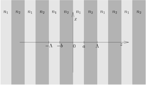
It is an easy task to calculate reflection coefficient of a lattice built of dielectric layers, which extend towards infinity in and directions (where coordinate system is taken as shown in Fig. 1). Following [7], in every layer, for each of two polarizations, a solution of Maxwell equations can be written as a superposition of two plane waves:
| (1) |
where stands for the number of the layer and
| (2) |
These plane waves are bound with plane waves in the next layers by continuity conditions, which can be written as a matrix equation ([7, 8, 9]):
| (3) |
where is the continuity condition matrix: {subequation}
| (4) |
| (5) |
where is the wave vector’s component in the th layer, is the th layer’s width and is the th layer’s refractive index (more precisely, Eq. (3) is a relation between amplitudes of fields in different points of space – left edges of layers). Amplitudes of plane waves outside the lattice are therefore related to each other:
| (6) |
If is an amplitude of the plane wave incident on the lattice, then corresponds to the plane wave reflected in the infinity. This reflection does not occur, hence . Therefore:
| (7) |
where
| (8) |
and as a result:
| (9) |
The reflection coefficient of the whole lattice is then given by
| (10) |
with the assumption, that amplitudes and describe incident and reflected plane waves in a “virtual” layer with the same refraction coefficient as the external medium and width . The above expression is purely analytical, though for lattices with diversified layers it would take a very complicated form if written as an explicit function of wave vector, polarization and lattice parameters, which are hidden in and .
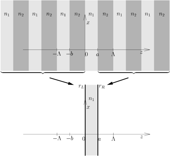
Having derived (10), we can calculate reflection coefficient of any number of dielectric layers, what allows us to treat any randomly selected layer of a lattice as an effective resonator. The idea of this model is presented in Fig. 2. Formally, a lattice can be treated as two lattices and the layer joined together. It is possible to replace the lattices on both sides of the layer with mirrors having the same reflection coefficients and , where denotes polarization.
3 Mode spectrum
Let be a plane wave exciting a resonator limited by two parallel planes with reflection coefficients and (direction of this vector determines polarization of the wave). Because of reflections, there appears in the resonator an effective plane wave . We introduce an operator , which establishes a relation between them ([10, 11]):
| (11) |
We call a plane wave with polarization and wave vector a mode of the resonator, if it is an eigenvector of :
| (12) |
Eigenvalue is proportional to mode spectrum , which we define as:
| (13) |
Mode spectrum describes distribution of modes in wave vector domain, which is equivalent to frequency and direction of propagation. We consider the following relation between mode spectrum and density of states (DOS):
| (14) |
In free space no reflections occur and therefore the operator is an identity, with all eigenvalues equal to . Hence, mode spectrum is constant in free space, and with taken normalization we obtain from (14) valid and well known formula for DOS in free space:
| (15) |
Let be a mode of the considered resonator. If the amplitude of the excitation is , to find the amplitude of the effective plane wave one has to sum all the reflected waves:
| (16) |
where is the resonator’s width. The second sum arises because continuity conditions apply on both mirrors, and it can be easily checked, that for a plane wave incident on a plane between two different media the change of sign of (assuming that axis is perpendicular to the plane) causes the reflection coefficient to become its conjugate. It follows, that mode spectrum for the resonator is described with the formula:
| (17) |
where reflection coefficients depend on polarization and wave vector.
4 Defects in 1D photonic crystal
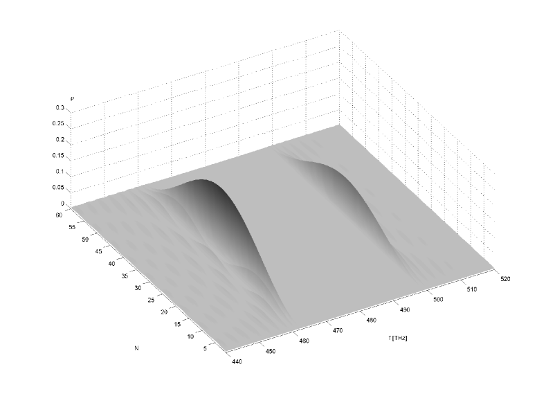
Formula (17) allows to analyze properties of layers of a lattice, in a particular case – a 1D photonic crystal. In this kind of structure there appear photonic band gaps, regions of frequency for which no mode is allowed. In terms of mode spectrum a photonic band gap is a region, for which mode spectrum is equal to . However, in a structure built of finite number of layers it is not strictly possible, because the structure is not able to fully eliminate coupling with electromagnetic field outside of it. Mode spectrum of a perfect photonic crystal in the region of a band gap for perpendicular incidence () is shown in Fig. 3 versus frequency and the number of elementary cell in which there is the layer, for which the calculation has been made. For simplicity, it has been assumed that the crystal is surrounded by a uniform medium with refractive index .
As it can be seen in Fig. 3, for elementary cells near the middle of the crystal mode spectrum is practically equal to in the gap with maximal values at both edges of the gap. Outside the gap mode spectrum fluctuates around the free space value. It means, that the layers are resonators with resonant frequencies at the gap edges. For layers near the crystals edge there is only a slight difference between mode spectrum of the layer and a uniform medium (which is constant in the latter case), because they are resonators with a very low quality and do not impose a significant change of an amplitude of a plane wave.
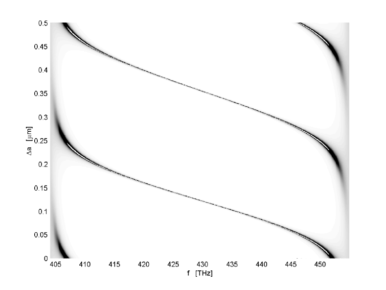
Introducing a defect of width to a layer results in an appearance of a defect mode. The size of the defect determines at which frequency does it happen – see Fig. 4 – obviously, because a resonant frequency of a resonator depends on its width. However, the defect mode appears only in a certain number of layers near the defected one, because electromagnetic field with frequency from a band gap has an envelope which vanishes in consecutive layers – it has a limited range of penetration, hence the defect has no noticeable influence on mode structure of layer which is sufficiently distant. This behaviour is depicted in Fig. 5 (values on -axis in this figure are limited).
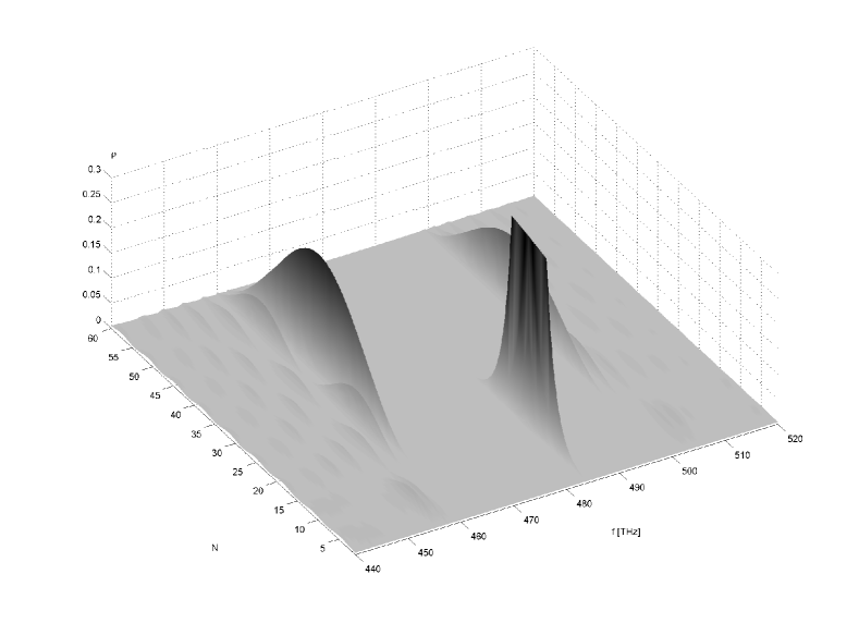
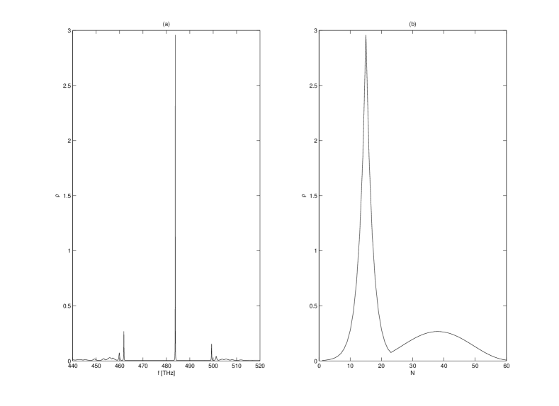
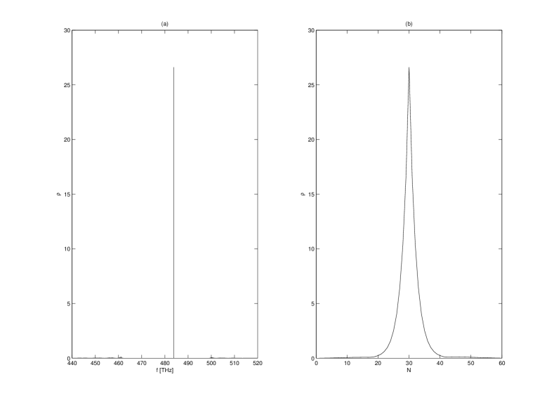
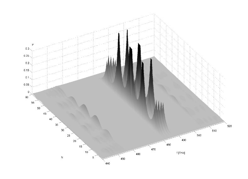
Figure 6 shows maximal values of mode spectrum for each frequency and in each layer. It can be seen, that the defect introduces much higher values of mode spectrum than the edges of the band gap. Modification of mode spectrum depends on which layer is defected – a similar graph for a defect in the middle of the photonic crystal is shown in Fig. 7. In this case the defect mode frequency is the same, but values of mode spectrum associated with the defect are even higher.
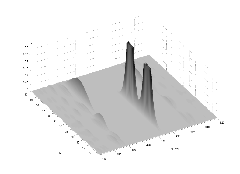
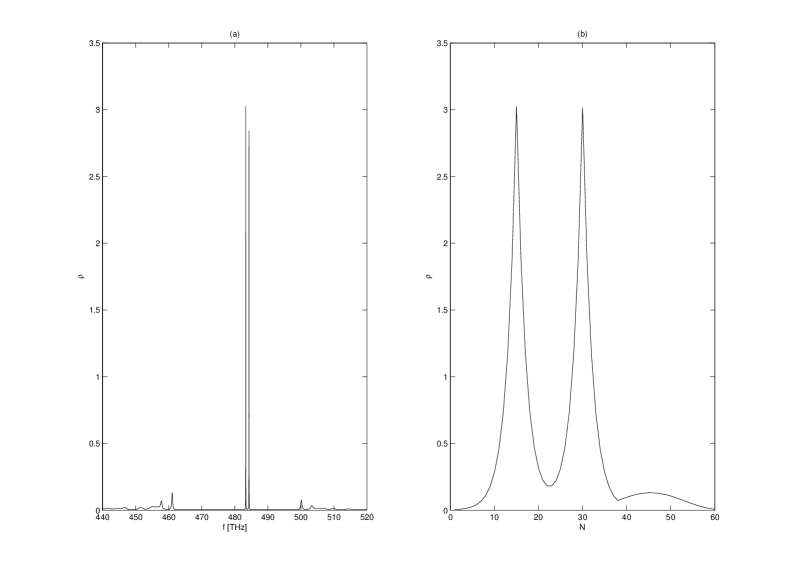
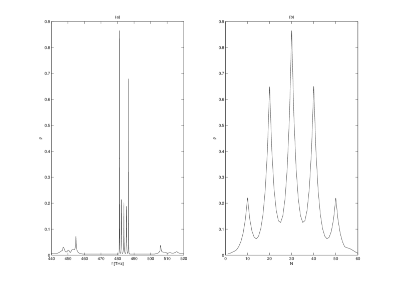
If a photonic crystal has two defected layers, then there appear two regions in which influence of defect modes is significant. Overlap of these regions results in two defect modes, with two different frequencies, instead of one. This case is shown in Fig. 8 and maximal values of mode spectrum are plotted in Fig. 9. Adding more defect leads to further splitting of the band gap by a new defect band – see Figs. 10 and 11.
5 Conclusions
In this paper we have analyzed the influence of defects in a 1D photonic crystal on the density of states and spontaneous emission, in both spacial and frequency domains. We have used the effective resonator model and derived an analytical expression for mode spectrum. With the help of this relation the presented numerical results revealing properties of 1D photonic crystal with defects have been obtained. In particular, it has been shown that a single defect has local character and its influence on mode structure diminishes with the distance from the defect position.
Acknowledgements.
Project granted by the Ministry of Education and Science in Poland, project no 3 T11B 069 28. The authors are members of the Sixth European Union Framework Program for Research and Technological Development (FP6) – Network of Excellence on Micro-Optics “NEMO”.References
- [1] E. Yablononovitch. Inhibited spontaneous emission in solid-state physics and electronics. Phys. Rev. Lett., 58:2059, 1987.
- [2] S. John. Strong localization of photons in certain disordered dielectric superlattices. Phys. Rev. Lett., 58:2486, 1987.
- [3] S.-Y. Zhu, H. Chen, and H. Huang. Quantum interference effects in spontaneous emission from an atom embedded in a photonic band gap structure. Phys. Rev. Lett., 79:205, 1997.
- [4] Y. Yang, M. Fleischhauer, and S.-Y. Zhu. Spontaneous emission in a photonic crystal near the band edge: Field versus population dynamics. Phys. Rev. E, 68:015602–1, 2003.
- [5] N. Kawai, M. Wada, and K. Sakoda. Limits on quality factors of localized defect modes in photonic crystals due to dielectric loss. J. Appl. Phys., 84:6299, 1998.
- [6] R. K. Lee, O. Painter, B. Kitzke, A. Scherer, and A. Yariv. Emission properties of a defect cavity in a two-dimensional photonic bandgap crystal slab. J. Opt. Soc. Am. B, 17:629, 2000.
- [7] P. Yeh, A. Yariv, and C. Hong. Electromagnetic propagation in periodic stratified media. i. general theory. J. Opt. Soc. Am., 67:423, 1977.
- [8] J. D. Jackson. Classical electrodynamics. J. Wiley, 1975.
- [9] A. Rudziński. Problem of spontaneous emission process in photonic crystals. B.Sc. thesis, Warsaw University of Technology, 2003.
- [10] A. Rudziński. Problem of density of states of electromagnetic field in two-dimensional photonic crystals. M.Sc. thesis, Warsaw University of Technology, 2004.
- [11] A. Rudziński, A. Tyszka-Zawadzka, and P. Szczepański. Simple model of the density of states in 1d photonic crystal. In Proc. of SPIE, volume 5950, 2005.