Single-Gate Accumulation-Mode InGaAs Quantum Dot with a Vertically Integrated Charge Sensor
Abstract
We report on the fabrication and characterization of a few-electron quantum dot controlled by a single gate electrode. Our device has a double-quantum-well design, in which the doping controls the occupancy of the lower well while the upper well remains empty under the free surface. A small air-bridged gate contacts the surface, and is positively biased to draw laterally confined electrons into the upper well. Electrons tunneling between this accumulation-mode dot and the lower well are detected using a quantum point contact (QPC), located slightly offset from the dot gate. The charge state of the dot is measured by monitoring the differential transconductance of the QPC near pinch-off. Addition spectra starting with were observed as a function of gate voltage. DC sensitivity to single electrons was determined to be as high as %, resulting in a signal-to-noise ratio of with an equivalent noise bandwidth of kHz. Analysis of random telegraph signals associated with the zero to one electron transition allowed a measurement of the lifetimes for the filled and empty states of the one-electron dot: ms and ms, respectively, for a device with a nm AlInAs tunnel barrier between the two wells.
Semiconductor quantum dots have been a subject of recent interest, due in part to their potential use in quantum information processing applications DiVincenzo ; Kouwenhowen ; Elzerman ; Hanson . The electron spin in a magnetic field is a promising two-level quantum system in which to represent the qubit, as decoherence times can be quite long (tens to hundreds of milliseconds), particularly in a Si-based implementation Eriksson ; Tyryshkin .
In this paper, we describe the practical realization of a novel device geometry, similar in some respects to devices described in Refs. Vrijen ; IEEE ; Kosaka ; Zaitsu , in which the quantum dot and the readout channel are integrated in a vertical structure. In our case, the quantum dot is located above the channel instead of adjacent, as is the case for laterally-depleted dots Petta . The design is particularly simple in that it uses a single gate electrode to define the dot and control its occupancy. No etching is necessary to define the dot.
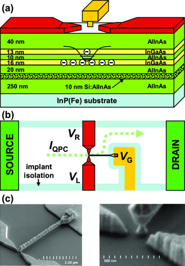
The heteroepitaxial stack, doping profile, and electrode layout were optimized in a comprehensive theoretical effort described partly in Ref. Caflisch . A schematic diagram detailing the layer structure and device design is shown in Fig. 1(a). The samples are doped so that away from the gates, under the free surface, the upper well is fully depleted and the lower well contains a two-dimensional electron gas (2DEG). Placement of the dopant supply layer below the two quantum wells was found to result in a more robust design, requiring less control of the total doping to achieve the desired band profile. The 2DEG in the lower well also serves as a source of electrons for the dot.

The quantum dot is located at the center of an implant-isolated region contacted at each end with sintered ohmic contacts. Lateral depletion gates under reverse bias form a quantum point contact (QPC) in the lower well near the dot. The quantum dot is formed in the upper well by placing the dot gate in forward bias (hence, our use of the term accumulation mode) to locally push the conduction band in the upper well below the Fermi level of the 2DEG. Electrons can then tunnel into the potential well created by the gate when the 2DEG Fermi level aligns with the quantum states of that localized potential. The typical device we studied was a nominally nm diameter dot gate within nm of the QPC.
The sample was grown on a in. semi-insulating, -oriented InP substrate in a gas source MBE system. Doping was adjusted to provide a K sheet electron density of cm; mobility was measured to be cm/volt-sec. Figure 1(b) shows the layout looking down from above. The air-bridge extended from the gate feed [yellow region surrounded by implant isolation in Fig. 1(b)], over the semiconductor, contacting it at only one point near the center of the QPC [see also Fig. 1(c) for scanning electron micrograph images of representative devices]. The gate feed was defined using standard optical lithography, whereas the QPC, the dot gate, and the air-bridge were formed using two e-beam lithography and metallization steps.

Devices were introduced into a top-loading 3He system and tested at temperatures below mK. No magnetic fields were used in the experiments reported here. We measured the differential transconductance () of the QPC using a low-noise transimpedance amplifier (TIA) and standard lock-in techniques. The differential transconductance signal was generated by applying a source-drain bias of V across the QPC and adding a small AC modulation to the DC dot gate voltage, . The lock-in then measured the QPC current at the applied frequency.
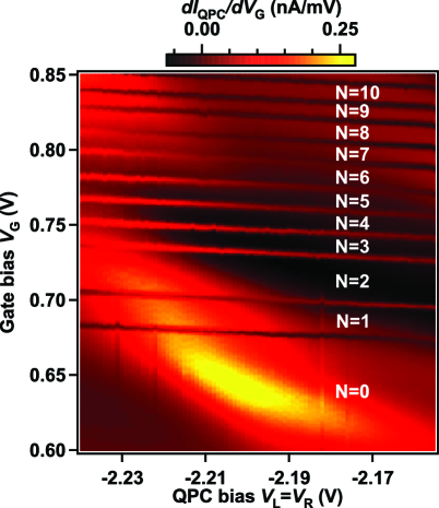
Figure 2 shows the amplitude of the in-phase component of the differential transconductance for a typical device, measured near QPC pinch-off, as a function of and the QPC bias (for the ‘left’ and ‘right’ QPC gates). For each QPC bias, the gate voltage was swept from to V, causing electrons to tunnel sequentially from the lower well into the upper well at particular values of bias for which the 2DEG Fermi level aligned with the quantum states of the dot. Transitions are indicated by a dip (peak) when the background transconductance signal is positive (negative). The dot occupancy , labeled in white, is evident from the fact that no transitions are observed below V despite the QPC still being sensitive to changes in the local electrostatic charge configuration. Furthermore, the tunneling rate is largely independent of all gate biases used in the experiment, in contrast to the more common depletion-gated devices in which pinch-off of the tunnel barriers is always a concern when the dot is nearly empty Elzerman ; Ciorga .

From the slope of the transition lines, we obtained the ratio, , for the gate to QPC capacitances, confirming the dot potential was primarily controlled by a single gate. The large voltage gap at is a fingerprint of strong electron quantization in the dot potential, with the scale of orbital energies being comparable to the electrostatic charging energies. Real-space few-electron simulations of the ground state filling spectrum were performed using the grown epitaxial structure and final metal dimensions. Excellent agreement was found between the simulated and measured voltage gaps providing an estimate for the charging energy of meV.
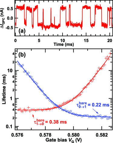
In another experiment, we digitized the output of the TIA as a function of time for different values of . On resonance, random telegraph signals (RTS) were observed for each transition. Figure 3(a) shows a representative time trace of the QPC current for the electron transition after optimizing the QPC bias for maximum sensitivity. The red curve is the output of the TIA after being low-pass filtered by a double-pole buffered RC filter set to have a –% rise time of s. The measured equivalent noise bandwidth in this configuration was found to be kHz, resulting in a total of pA of noise. Single electron occupation changes resulted in a pA change in the nA DC current (% sensitivity, ). Figure 3(b) is a plot of the average lifetimes (average of the times spent in the high and low current states, respectively) for the electron transition as a function of ; the filling voltage is reduced from that of Fig. 2 because the data were taken after a separate cooldown. For each gate bias, a histogram of the individual tunneling times was generated from seconds of current data, sampled every s. A simple thresholding procedure was used to determine when loading and unloading events had occurred. The tunneling times were confirmed to obey Poisson statistics by both fitting the distribution of tunneling times to an exponential and observing that the average lifetime was equal to the standard deviation. The solid lines are fits to the functions and , where is the lever arm of the top-gate to dot potential Weis , is Boltzmann’s constant, and is the gate bias that aligns the chemical potentials of the empty dot and the lower well. The fitting parameters, and , are the minimum lifetimes corresponding to loading and unloading of the one-electron dot, respectively. The fits yield mV, V, and minimum lifetimes of ms and ms for loading and unloading, respectively. Loading is approximately a factor of two faster than unloading due to the fact that both spin states are available to load into when the dot is empty. These results were obtained for a dot with a 10 nm Al0.48In0.52As tunnel barrier between the two wells.
In summary, we have demonstrated the creation of a well-controlled, few-electron quantum dot in an accumulation mode device using a single surface gate placed in forward bias. We have also demonstrated single-shot readout of the charge state of these dots using an adjacent QPC formed in the lower well as a charge sensor. This device layout offers several advantages over existing designs. Unlike other vertically-oriented devices formed by etching pillar structures, it should be straightforward to place these dots in close proximity and control their coupling through the use of one additional surface gate placed between the dot gates. Unlike depletion-gate geometries that require several gates to form even a single dot, our approach forms the dot and controls electron occupancy with a single, forward-biased gate.
Acknowledgements.
The authors gratefully acknowledge Profs. HongWen Jiang and Robert Schwartz for many useful discussions. Sponsored by United States Department of Defense. The views and conclusions contained in this document are those of the authors and should not be interpreted as representing the official policies, either expressly or implied, of the United States Department of Defense or the U.S. Government. Approved for public release, distribution unlimited.References
- (1) D. Loss and D. P. DiVincenzo, Phys. Rev. A 57, 120 (1998).
- (2) L. P. Kouwenhoven, D. G. Austing, and S. Tarucha, Rep. Prog. Phys. 64, 701 (2001).
- (3) J. M. Elzerman, R. Hanson, L.H.W. van Beveren, S. Tarucha, L.M.K. Vandersypen, and L.P. Kouwenhoven, Lect. Notes Phys. 667, 25 (2005).
- (4) R. Hanson, L. P. Kouwenhoven, J. R. Petta, S. Tarucha, and L. M. K. Vandersypen, Rev. Mod. Phys. 79, 1217 (2007).
- (5) M. A. Eriksson, M. Friesen, S. N. Coppersmith, R. Joynt, L. J. Klein, K. Slinker, C. Tahan, P. M. Mooney, J. O. Chu, and S. J. Koester, Quantum Information Processing 3, 133 (2004).
- (6) A. M. Tyryshkin, S. A. Lyon, A. V. Astashkin, and A. M. Raitsimring, Phys. Rev. B 68, 193207 (2003).
- (7) R. Vrijen, E. Yablonovitch, K. Wang, H. W. Jiang, A. Balandin, V. Rowchowdhury, T. Mor, and D. DiVincenzo, Phys. Rev. A 62, 012306 (2000).
- (8) E. Yablonovitch, H. W. Jiang, H. Kosaka, H. D. Robinson, D. S. Rao, T. Szkopek, Proc. IEEE 91, 761 (2003).
- (9) H. Kosaka, D. S. Rao, H. D. Robinson, P. Bandaru, K. Makita, and E. Yablonovitch, Phys. Rev. B 67, 045104 (2003).
- (10) K. Zaitsu, Y. Kitamura, K. Ono, and S. Tarucha, Appl. Phys. Lett. 92, 033101 (2008).
- (11) J. R. Petta, A. C. Johnson, J. M. Taylor, E. A. Laird, A. Yacoby, M. D. Lukin, C. M. Marcus, M. P. Hanson, and A. C. Gossard, Science 309, 2180 (2005).
- (12) R. E. Caflisch, M. F. Gyure, H. D. Robinson, and E. Yablonovitch, SIAM J. Appl. Math. 65, 1285 (2005)
- (13) M. Ciorga, A.S. Sachra jda, P. Hawrylak, C. Gould, P. Zawadzki, S. Jullian, Y. Feng and Z. Wasilewski, Phys. Rev. B 61, R16315 (2000).
- (14) J. Weis, R. J. Haug, K. v. Klitzing, and K. Ploog, Phys. Rev. B 46, 12837 (1992).