Ring-shaped luminescence patterns in a locally photoexcited electron-hole bilayer
Abstract
We report the results of molecular dynamics simulation of a spatiotemporal evolution of the locally photoexcited electrons and holes localized in two separate layers. It is shown that the ring-shaped spatial pattern of luminescence forms due to the strong in-layer Coulomb interaction at high photoexcitation power. In addition, the results predict (i) stationary spatial oscillations of the electron density in quasi one-dimensional case and (ii) dynamical phase transition in the expansion of two-dimensional electron cloud when threshold electron concentration is reached. A possible reason of the oscillations and a theoretical interpretation of the transition are suggested.
pacs:
71.35.–y, 73.50.Gr, 73.63.-b, 78.67.DeExciton systems in semiconductor nanostructures can provide an unique opportunity to obtain nonequilibrium superfluid transition in solids Mos ; KK ; Loz ; ex_sup . Indeed, a remarkable phenomenon has been experimentally discovered in the system of interwell excitons in GaAs/AlGaAs double quantum wells (QWs) But_ring : local off-resonant photoexcitation of electrons (e) and holes (h) gives rise to a macroscopic ring-shaped pattern of the luminescence spatial distribution when the excitation power is above some threshold value. The similar effects were observed later in other systems snoke_nat ; Tim ; stern .
The first theoretical explanation of the phenomenon was suggested BLS ; theor ; Ha within the diffusive transport model (DTM). However, the model is not applicable to the experiments But_ring for the derivation of the ring radius com . In particular, the ring radius is derived within the DTM as
| (1) |
where is the diffusion coefficient for electrons, is the equilibrium two-dimensional (2D) electron density, is the stationary photoexcitation power, and the electron depletion length BLS . According to the model BLS , the diffusion of holes is the only reason why they move out of the laser excitation spot. However, according Eq.(1) the ring radius does not depend on the hole diffusion coefficient (in BLS is in the exponent also), i.e. the ring forms even if all holes are left into the excitation spot (). This clearly unphysical result is not a consequence of the limiting case , but is valid in the general case Ha . Moreover, the DTM can not explain in principle the condition on the excitation power, i.e. that the external ring appears only when the power exceeds some critical value, But_ring . So the development of a different theory of the ring pattern formation is necessary.
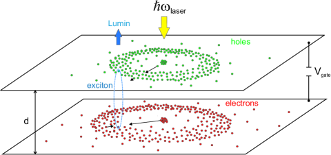
Here we present both quasi one-dimensional (1D) and 2D simulations of the spatiotemporal dynamics of optically generated electrons and holes that are located in two coupled layers (Fig.1). We show that due to (i) large in-layer Coulomb interaction in the pumping region at high excitation intensities and (ii) essential difference in mobilities and effective masses for electrons and holes in GaAs, a macroscopic spatial separation of the electron and hole densities appears naturally. In contrast to the previous theoretical studies BLS ; theor ; Ha , the in-plane distributions for electrons and holes are found self-consistently. The distribution of holes is located much closer to the excitation spot than the electron one, and their narrow overlap gives large ring-shaped luminescence pattern. We also find that the dependence of exciton formation rate on the electron-hole relative velocity is crucial for the ring-shaped pattern formation. More surprisingly, we have clearly observed stationary spatial oscillations of the electron density outside the luminescence ring in 1D case. A possible origin of the oscillations is a kinetic instability of two interacting electron counter flows: faster flow from the center to the periphery and slower back flow from the periphery to the luminescence region due to the depletion of electron density there.

Model.—To describe the dynamics of hot electrons and holes, we use the Newton equations of motion combined with the exciton formation condition. The dimensionless equations read
| (2) | ||||
where vectors and are in-plane positions of -th electron and -th hole (); is the interlayer distance. The left-hand side of Eqs.(2) accounts electron and hole inertia and momentum damping (mainly due to interaction with acoustic phonons), while the right-hand side describes the in-layer electron-electron and hole-hole Coulomb repulsion as well as the interlayer electron-hole attraction. Hereafter, we normalized time by and all distances by , where and are electron charge and mobility, respectively, is effective electron mass and is dielectric constant of the layers. The coefficients in Eqs.(2) are and . To estimate the parameters, we use well-known experimental values for high-quality undoped GaAs/AlGaAs QWs note0 getting , , s, cm that gives for interlayer spacing of about cm But_rev .
Stationary optical excitation of electrons and holes was modeled by generating the particles in random positions inside the excitation spot of radius with rate . Initial velocities of electrons and holes were also chosen randomly within intervals and with ratio to allow the momentum conservation for each e-h pair created. During the dynamical evolution of the carriers, an exciton formation happened if an electron and a hole were close enough to each other, , where is a phenomenological in-layer exciton radius a_ex , and their relative velocity was smaller than some critical value Vc . To simplify the calculations, we did not consider the exciton dynamics and neglected the interaction of charge carriers with dipole excitons. It means that as soon as an electron and a hole had formed an exciton, their dynamics was no longer considered and the position of the formation event was recorded as a position of photon emission. In addition, due to the inevitable restrictions in computational power we were able to simulate interacting particles. For this reason we had to increase the value of .
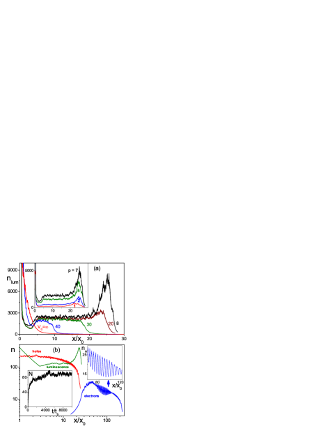
Results for 1D case.—The results of extensive 1D simulations of Eqs.(2) combined with the exciton formation condition are shown in Fig.2. The stationary luminescence density has a large distant peak that correlates with the ring-shaped pattern observed experimentally But_ring ; snoke_nat ; stern ; BLS ; But_new . It is remarkable that the smaller critical relative velocity for the exciton formation, the larger both the peak amplitude and the distance between the peak position and the excitation spot in the center (Fig.2a). Indeed, at extremely large , when an exciton is formed as soon as the instant distance between an electron and a hole is small enough, the luminescence decreases monotonically from the excitation spot. For the finite but still high critical velocities a broad plateau-like maximum appears out of the centre in the luminescence pattern. Finally, a narrow high peak of luminescence located on the external plateau edge far away from the excitation spot develops at lower . To uncover the origin of this peak, we plot density distributions for electrons and holes (Fig.2b). It is seen that the hole distribution is located much closer to the excitation spot than the electron one. The luminescence peak forms in the region where electron and hole densities overlap. In addition, the electron density exhibits pronounced spatial oscillations beyond the luminescence peak (Fig.2b). They depend on optical pumping parameters: e.g., the characteristic period of the oscillations is proportional to , where is pumping rate. By turning off interlayer electron-hole interaction, we have concluded that the oscillations originate due to the in-layer electron-electron interaction. In particular, they can be caused by a kinetic instability of two interacting electron counter flows: the flow of hot electrons expanding from the center meets the returning flow of electrons from the steady electron cloud at the periphery. The back flow can originate from the depletion of the density of slow electrons in the luminescence region due to the exciton formation. Nevertheless, a detailed understanding of the underlying physical mechanism of the electron density oscillations still requires further studies. The dependence of the luminescence peak on the electron-hole creation rate (inset in Fig.2a) has shown that though the peak height increases with , its position is almost independent on for 1D case. This behaviour differs from that observed experimentally for 2D samples But_ring , where the luminescence ring radius grows essentially with the increase of pumping intensity. The difference poses a question of modeling the full-value 2D expansion of photoexcited electron-hole plasma.
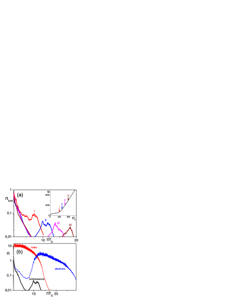
Results for 2D case.—Due to the quadratic increase of the number of particles, in 2D case without a boundary (Fig.3) the stationary state was not reached for the expectation time, though a clear tendency to slow down was observed for the expansion of the electron distribution. Remarkably, however, that the luminescence ring-shaped pattern forms dynamically at , fastly expanding afterwards (Fig.3a) (cp. But_new ). Moreover, the spatiotemporal dynamics of the 2D electron density (not shown) has revealed very nontrivial details: at the electron cloud ejects a long ”tail” towards the outside of the excitation area. Due to the corresponding depletion of the internal part of the cloud, the in-layer separation between electron and hole distributions becomes more pronounced giving rise to a sharp luminescence ring in the bilayer plane.
To roughly understand why the dynamical transition occurs in 2D case, let us reduce Eqs.(2) to the case when the carrier distributions can be described only by collective ring coordinates , where . In the limit the equation of motion for the electron ring reads
| (3) |
where is a width of the electron ring. (For simplicity, we neglect the dependences and .) The first term in the right-hand side describes the interaction of electrons within the ring, while the second term originates from the electron-hole interaction. The logarithmic factor in the electron-electron interaction term is absent in 1D case. It results in a fast expansion of the electron ring for , i.e., when has amounted to some critical value.
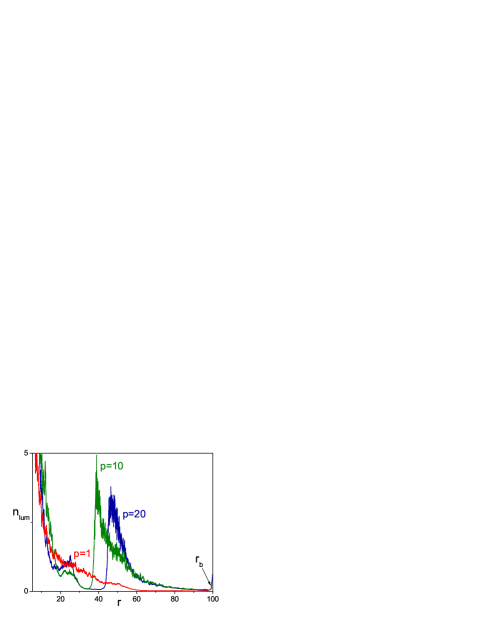
We have confirmed that the principle of the ring pattern formation in 2D case is the same as that in quasi 1D case: the luminescence peak appears at the narrow overlap of separated electron and hole density distributions (Fig.3b). Meanwhile, the electron density oscillations observed in quasi 1D case are absent in 2D case, even in the stationary state for the case with a boundary. In the latter case, we have also observed the onset of the luminescence ring at high enough pumping rate (Fig.4, cp. inset in Fig.2a) and the shift of the ring position to larger when increasing . The result correlates well with the experimental dependence (Fig.1a in But_ring ) for pumping powers slightly above threshold.


Qualitative picture.—The macroscopic electron-hole spatial separation and luminescence ring-shaped pattern formation can be explained as follows. At high photoexcitation power the carrier densities in the excitation spot quickly reach their critical values () when the repulsive in-layer Coulomb forces between particles become stronger than the attractive interlayer force. It leads to the appearance of in-layer electric fields ejecting the ”surplus” electrons and holes from the excitation spot region. Then the e-h densities in the spot grow to the critical values again and the ejection process recurs. Due to very high mobilities of the carriers in GaAs quantum wells at low temperature mob0 ; mob ; cp , the initial velocities of the ejected particles are also high. The absolute values of the velocities are restricted by the emission threshold of an optical phonon that gives cm/s note . In turn, the velocity ratio for the hot electrons and holes has the same order of magnitude as the ratio between their mobilities ( for GaAs/AlGaAs QWs at temperatures K mob .) Due to this, the electron distribution is mainly located much farther from the excitation spot than the hole one. During the in-plane expansion the electrons and holes cool down emitting acoustic phonons. In addition, their relative velocities decrease due to the interlayer Coulomb drag screen . Finally, the luminescence ring appears in the overlapping region between the stationary densities of the slowed electrons and holes. Note that at typical electron-acoustic phonon scattering time s phon one comes to the promising estimate for the ring radius mm (cp. But_ring ; cp ).
Conclusion.—We have simulated a spatiotemporal evolution of the locally photoexcited electrons and holes localized in two separate layers. In contrast to previous theoretical studies BLS ; theor ; Ha ; But_new , we have shown that both in-plane spatial separation of electrons and holes and the ring-shaped luminescence pattern are formed essentially due to the in-layer Coulomb repulsion. A specific reason for the separation is found to be the difference in electron and hole mobilities. In turn, a specific reason for the luminescence ring is the dependence of exciton formation probability on the electron-hole relative velocity. We also observed drastically different electron and hole dynamics in 1D and 2D cases and, more importantly, pronounced stationary spatial oscillations of the electron density in 1D case.
We thank A. S. Alexandrov, Yu. M. Kagan and F. V. Kusmartsev for helpful discussions.
References
- (1) S. A. Moskalenko, Sov. Phys. Solid State 4, 199 (1962).
- (2) L. V. Keldysh, A. N. Kozlov, Sov. Phys. JETP 27, 521 (1968).
- (3) Y. E. Lozovik, V. I. Yudson, JETP Lett. 22, 274 (1975).
- (4) A. V. Balatsky et al., Phys. Rev. Lett. 93, 266801 (2004); J. Kasprzak et al., Nature 443, 409 (2006).
- (5) L. V. Butov et al., Nature 418, 751 (2002).
- (6) D. Snoke et al. Nature 418, 754 (2002).
- (7) V. B. Timofeev, A. V. Gorbunov, J. Appl. Phys. 101, 081708 (2007).
- (8) M. Stern et al., Phys. Rev. Lett. 101, 257402 (2008).
- (9) L. V. Butov et al. Phys. Rev. Lett. 92, 117404 (2004);
- (10) R. Rapaport et al. Phys. Rev. Lett. 92, 117405 (2004); S. Denev et al. Solid State Commun. 134, 59 (2005); A. A. Chernyuk, V. I. Sugakov, Phys. Rev. B 74, 085303 (2006).
- (11) M. Haque, Phys. Rev. E 73 066207 (2006).
- (12) A. V. Paraskevov, arXiv:0902.3909v2.
- (13) We take typical cm2/(Vs) mob0 for temperatures K and electron densities cm-2 (excitation spot), for GaAs (see also note ) and mob .
- (14) L. V. Butov, J. Phys.: Condens. Matter 16, R1577 (2004).
- (15) Due to the finite interlayer distance , the exciton radius can be essentially larger than the Bohr radius of a purely 2D exciton ( cm for GaAs).
- (16) There are two critical relative velocities so one should choose the minimal value. One appears due to the finite interlayer distance , , where is e-h reduced mass. If the Fourier transform of interlayer Colulomb interaction potential drops as screen . At cm But_rev and in GaAs, cm/s. Another comes from the exciton formation condition: electron-hole scattering rate should not exceed carrier-acoustic phonon one, . Its estimate is , and . For s phon and cm-2 But_rev one gets cm/s.
- (17) S. Yang et al., arXiv:0908.2978v1.
- (18) H. L. Stormer et al., Phys. Rev. B 41, 1278 (1990); M. P. Lilly et al., Phys. Rev. Lett. 90, 056806 (2003).
- (19) J. A. Seamons et al., Appl. Phys. Lett. 90, 052103 (2007).
- (20) G. R. Facer et al., Phys. Rev. B 59, 4622 (1999).
- (21) To contribute to the transport, the value of photoexcited carrier velocity should be restricted by optical phonon emission, , where for GaAs is the optical phonon energy, and effective electron and heavy hole masses are and ( is bare electron mass). The estimates result in cm/s. The corresponding de Broglie wavelength of the carriers cm.
- (22) U. Sivan et al., Phys. Rev. Lett. 68, 1196 (1992).
- (23) T. Kawamura, S. Das Sarma, Phys. Rev. B 45, 3612 (1992); V. I. Fal’ko, Phys. Rev. B 47, 13585 (1993).