Signatures of Klein tunneling in disordered graphene p-n-p junctions
Abstract
We present a method for obtaining quantum transport properties in graphene that uniquely combines three crucial features: microscopic treatment of charge disorder, fully quantum mechanical analysis of transport, and the ability to model experimentally relevant system sizes. As a pertinent application we study the disorder dependence of Klein tunneling dominated transport in p-n-p junctions. Both the resistance and the Fano factor show broad resonance peaks due to the presence of quasi bound states. This feature is washed out by the disorder when the mean free path becomes of the order of the distance between the two p-n interfaces.
A realistic modeling of quantum transport in graphene Novoselov et al. (2004) has two main requirements: microscopic treatment of disorder and a fully quantum mechanical calculation of transport, taking into account the finite (but large with respect to the lattice constant) size of the samples. This is especially important close to the Dirac point Neto et al. (2009), the charge neutrality point at which transport is dominated by evanescent modes and conventional analytical methods fail, and for interference effects. In this letter we report on the first such calculation in a study of the resistance oscillations in a disordered graphene p-n-p junction which incorporates both realistic Coulomb disorder and quantum mechanical transport.
The physics of the p-n-p junction is governed by “Klein tunneling”, an effect first discovered in the context of a relativistic particle tunneling through a potential barrier with a height comparable to its rest energy Dombey and Calogeracos (1999). Since the occurrence of relativistic Klein tunneling is a crucial feature distinguishing graphene from ordinary electronic materials, a clear understanding of how to unambiguously observe Klein tunneling in realistic graphene samples, where disorder is unavoidably present, is important. In graphene, transmission through a potential barrier has a pronounced angular dependence, with perfect transmission for perpendicular incidence and a quick decrease of transmission probability for finite angle of incidence Ando et al. (1998). As a consequence, electrons can be confined within a single potential barrier, such as the p-n-p junction Silvestrov and Efetov (2007); Bardarson et al. (2009). Resonant tunneling through those confined states then leads to pronounced oscillations in the resistance as a function of system parameters Silvestrov and Efetov (2007); Shytov et al. (2008); Bardarson et al. (2009).
The existence of this phenomenon relies heavily on the presence of a well defined interface between the p and n regions. Early experiments failed to reproduce the predicted resistance oscillations Huard et al. (2007), presumably because of too much disorder. More recent experiments that seek to minimize the effects of disorder have been more successful Gorbachev et al. (2008); Stander et al. (2009); Young and Kim (2009). However a theoretical understanding of whether or to what extent these experiments are really observing Klein tunneling phenomena and the issue of the experimental conditions needed to see Klein tunneling unambiguously have remained open.
There exists strong evidence that disorder in current experiments is dominated by remote charged impurities Tan et al. (2007); Chen et al. (2008) invariably present in the graphene environment. Due to the long range character of the Coulomb potential of impurity and gate charges, all scattering potentials and charge densities in the graphene sheet vary slowly on the scale of the lattice constant. This fact leads to two simplifications that make an accurate modeling of current experimental setups Gorbachev et al. (2008); Stander et al. (2009); Young and Kim (2009) possible. First, the Thomas-Fermi-Dirac (TFD) self-consistent density functional method is sufficient to obtain the ground state carrier density in the presence of disorder Rossi and Das Sarma (2008); Rossi et al. (2009). Second, intervalley coupling can be neglected for a smooth scattering potential, so that one can model transport using the single valley Dirac Hamiltonian. The transfer matrix method of Refs. Titov, 2007 and Bardarson et al., 2007 is ideal for this purpose and can be used for experimentally relevant system sizes, as opposed to tight binding models which are generally limited to small system sizes.

Our calculation thus consists of two steps. In the first step the ground state carrier density and the corresponding screened Coulomb potential is obtained using the TFD approach Rossi and Das Sarma (2008). In the second step the resistance and Fano factor, the ratio of shot noise power and electrical current, are calculated using as an input into the fully quantum mechanical transfer matrix approach Titov (2007); Bardarson et al. (2007). We first describe the two steps of our method in more detail and then turn to the results.
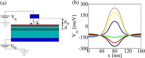
A schematic of the p-n-p junction under consideration is shown in Fig. 1a. A top gate of length is located a distance above the graphene layer — in an air-bridge setup the medium in between is air with dielectric constant . A back gate that controls the average carrier density is separated from the graphene by a SiO2 substrate (dielectric constant ). The effective dielectric constant in this setup is . Together, the voltages on these two gates define the junction. Examples of potential profiles are shown in Fig. 1b.
A number of charged impurities is trapped in the substrate and just below the graphene layer. We model this by a random distribution of impurity charges at a fixed distance with properties
| (1) |
with the average 2D charge impurity density.
In the TFD approximation, the ground state carrier density in the graphene layer is obtained by minimizing the energy functional
| (2) | |||||
with respect to . Here is the Fermi velocity for graphene,
| (3) | |||||
with , and the potentials induced by the impurity density and the top gate, respectively, and the chemical potential. is the exchange correlation energy (see Rossi and Das Sarma (2008); Polini et al. (2008) for details) which we include even though it gives only minor quantitative corrections to the transport properties of the p-n-p junction. The minimization is subject to the constraint , where is the area of the sample away from the top gate. The constraint is enforced self-consistently by varying . The electrostatic potential is expressed in terms of the top gate charge density ,
| (4) |
and is obtained self-consistently, for a fixed voltage difference between the top gate and graphene, , by requiring that in the region below the top gate where is the top gate capacitance.
The potential defines a scattering problem through the Dirac Hamiltonian
| (5) |
with the Pauli matrices. The Schrödinger equation generates a transfer matrix , which relates the wavefunction at to the one at , . In order to numerically calculate we divide the interval into equal subintervals of length and calculate the transfer matrix in each subinterval in the Born approximation. This gives Bardarson et al. (2007)
| (6) |
where
| (7) |
We then take the limit in which the Born approximation becomes exact. From the transfer matrix we calculate the matrix of transmission amplitudes, which in turn gives us the two terminal conductance and Fano factor as and .

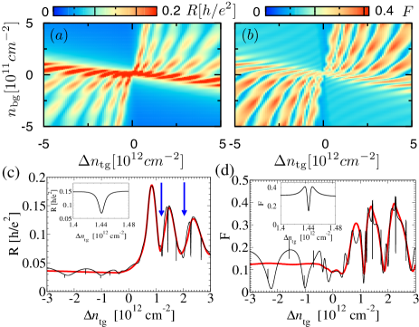
We now turn to our results. We first consider the clean case . By varying the top gate potential, the junction type can be varied from p-n-p to p-p-p (or n-p-n to n-n-n depending on the back gate voltage), as shown in Fig. 1b. The dependence of the resistance and Fano factor on the two gate voltages is shown in Fig. 2a-b. In the p-p-p (n-n-n) region of the upper left (lower right) corner the resistance is small compared to the resistance of the p-n-p (n-p-n) region of the upper right (lower left) corner. Pronounced oscillations in the resistance are seen in the p-n-p and n-p-n regions. The behavior of the Fano factor mostly follows that of the resistance.
The resistance oscillations can be understood as arising from resonances through quasi bound states inside the barrier created by the two p-n interfaces Silvestrov and Efetov (2007); Shytov et al. (2008); Bardarson et al. (2009). The larger the transverse momentum , the larger the incident angle for scattering off the barrier and the tunneling amplitude decreases. The broad oscillations arise from resonant tunneling of the few modes with smallest . Larger give rise to very narrow resonance seen in Fig. 2c-d, where we show a cross-section of Fig. 2a-b at a fixed value of the back gate voltage in a higher resolution. Since the positions and widths of the narrow resonances are sensitive to the transverse boundary conditions we also plot the smooth curves obtained by averaging over twisted boundary conditions. The weak oscillations in the p-p-p and n-n-n regions and the narrow resonances are absent after the averaging. Observation of the narrow resonances will thus require very well defined edges. The double peak structure of the Fano factor resonances reflects the increase of the transmission probability from zero to one and back to zero and the fact that the Fano factor of a perfectly transmitted mode is zero.
In contrast to the narrow resonances the resistance minima for the broader oscillations do not depend on boundary conditions and can be estimated by a semiclassical argument Silvestrov and Efetov (2007). One can think of the p-n-p junction as a Fabry-Perot etalon in which waves scattered off the two p-n interfaces interfere destructively if the WKB phase
| (8) |
with the turning points defined by the condition , . The positions of the resistance minima that follow from this argument are indicated by arrows in Fig. 2.
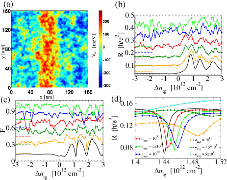
We now consider the effect of disorder. A single realization of the scattering potential in a disordered p-n-p junction is shown in Fig. 3a. For realistic impurity concentrations, the correlation length of is nm Rossi and Das Sarma (2008); Zhang et al. (2009). While one can still clearly make out the different and regions in the presence of disorder, the boundary between the two is no longer as sharp, leading to a weaker confinement of particles inside the barrier. The effects of Klein tunneling are thus expected to be suppressed.

Figures 3b-c give the transport properties as a function of top gate voltage for a single disorder realization and for different impurity densities. Mesoscopic fluctuations due to the disorder are superimposed on the oscillations from the Klein tunneling. As the impurity strength increases these fluctuations become stronger, eventually dominating the signal. The Fano factor is more sensitive to disorder than the resistance. The effect of disorder on a narrow resonance is shown in Fig. 3d.
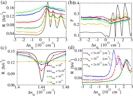
In Fig. 4 we show the disorder averaged resistance and Fano factor, where the average was taken over disorder realizations. We find that the clean limit broad quantum oscillations survive for impurity densities up to cm-2 while the narrow resonances disappear at cm-2. We do emphasize that for weak enough disorder the narrow resonances will be present, and it is therefore conceivable that they may actually be observed at low enough temperatures, when the phase coherence length is much larger than the system size.
As in the case of the single disorder realization, the dependence of the Fano factor on the disorder strength is similar to that of the resistance. The dependence of the resistance on the back gate voltage for a fixed impurity density is shown in Fig. 4d. The main effect of the back gate is an overall reduction of the resistance and a shift of the top gate density at which the central region changes polarity.
One expects impurity scattering effects to start dominating the ballistic oscillations when the mean free path becomes comparable to the sample width (for the narrow resonances) or the length of the central region (for the broad oscillations). The mean free path can be estimated through its relation to the conductivity , , where is the Fermi wavevector. Away from the Dirac point, Nomura and MacDonald (2006), where is a known function of and only [] Adam et al. (2007). Setting and using the impurity densities quoted above, we find that the narrow resonances vanish for nm, which is the same order of magnitude as expected. The impurity density at which the broad oscillations disappear corresponds to a mean free path nm. This is roughly the same as the length between the two p-n interfaces, see Fig. 1, and consistent with the experimental results of Refs. Gorbachev et al., 2008 and Stander et al., 2009.

In summary, we have presented a powerful theoretical method that is generally applicable to transport problems in realistic graphene samples where the disorder is dominated by charge impurities and transport properties need to be obtained fully quantum mechanically. We have applied this method to understand the effects of disorder on transport through p-n-p junctions. The crossover from the ballistic transport governed by Klein tunneling, to the disordered diffusive transport is found to take place as the mean free path becomes of the order of the distance between the two p-n interfaces consistent with recent experiments Gorbachev et al. (2008); Stander et al. (2009).
We thank S. Adam, E. H. Hwang, and in particular L. S. Levitov for discussions. The numerical calculations have been performed on the University of Maryland High Performance Computing Cluster (HPCC). This work is supported by US-ONR and NSF-NRI, by the NSF under grant no. DMR 0705476, and by the Humboldt Foundation. JHB thanks the Dahlem Center at FU Berlin for hospitality.
References
- Novoselov et al. (2004) K. S. Novoselov et al., Science 306, 666 (2004).
- Neto et al. (2009) A. H. Castro Neto et al., Rev. Mod. Phys. 81, 109 (2009).
- Dombey and Calogeracos (1999) N. Dombey and A. Calogeracos, Phys. Rep. 315, 41 (1999).
- Ando et al. (1998) T. Ando, T. Nakanishi, and R. Saito, J. Phys. Soc. Japan 67, 2857 (1998); M. I. Katsnelson, K. S. Novoselov, and A. K. Geim, Nat. Phys. 2, 620 (2006); V. Cheianov and V. Fal’ko, Phys. Rev. B (2006a).
- Silvestrov and Efetov (2007) P. G. Silvestrov and K. B. Efetov, Phys. Rev. Lett. 98, 016802 (2007).
- Bardarson et al. (2009) J. H. Bardarson, M. Titov, and P. W. Brouwer, Phys. Rev. Lett. 102, 226803 (2009).
- Shytov et al. (2008) A. V. Shytov, M. S. Rudner, and L. S. Levitov, Phys. Rev. Lett. 101, 156804 (2008).
- Huard et al. (2007) B. Huard et al., Phys. Rev. Lett. 98, 236803 (2007); J. R. Williams, L. DiCarlo, and C. M. Marcus, Science 317, 638 (2007); B. Özyilmaz et al., Phys. Rev. Lett. 99, 166804 (2007).
- Gorbachev et al. (2008) R. V. Gorbachev, A. S. Mayorov, A. K. Savchenko, D. W. Horsell, and F. Guinea, Nano Letters 8, 1995 (2008).
- Stander et al. (2009) N. Stander, B. Huard, and D. Goldhaber-Gordon, Phys. Rev. Lett. 102, 026807 (2009).
- Young and Kim (2009) A. F. Young and P. Kim, Nat. Phys. 5, 222 (2009).
- Tan et al. (2007) Y.-W. Tan et al., Phys. Rev. Lett. 99, 246803 (2007).
- Chen et al. (2008) J. H. Chen et al., Nature Physics 4, 377 (2008).
- Rossi and Das Sarma (2008) E. Rossi and S. Das Sarma, Phys. Rev. Lett. 101, 166803 (2008).
- Rossi et al. (2009) E. Rossi, S. Adam, and S. D. Sarma, Phys. Rev. B 79, 245423 (2009).
- Titov (2007) M. Titov, Europhys. Lett. 79, 17004 (2007).
- Bardarson et al. (2007) J. H. Bardarson, J. Tworzydlo, P. W. Brouwer, and C. W. J. Beenakker, Phys. Rev. Lett. 99, 106801 (2007).
- Polini et al. (2008) M. Polini, A. Tomadin, R. Asgari, and A. MacDonald, Phys. Rev. B 78, 115426 (2008).
- Zhang et al. (2009) Y. Zhang, V. W. Brar, C. Girit, A. Zettla, and M. F. Crommie, Preprint arXiv:0902.4793v1 (2009).
- Nomura and MacDonald (2006) K. Nomura and A. H. MacDonald, Phys. Rev. Lett. 96, 256602 (2006); T. Ando, J. Phys. Soc. Jpn. 75, 074716 (2006); V. Cheianov and V. Fal’ko, Phys. Rev. Lett. 97, 226801 (2006b).
- Hwang et al. (2007) E. H. Hwang, S. Adam, and S. Das Sarma, Phys. Rev. Lett. 98, 186806 (2007).
- Adam et al. (2007) S. Adam, E. H. Hwang, V. M. Galitski, and S. Das Sarma, Proc. Natl. Acad. Sci. USA 104, 18392 (2007).