A scalable control system for a superconducting adiabatic quantum optimization processor
Abstract
We have designed, fabricated and operated a scalable system for applying independently programmable time-independent, and limited time-dependent flux biases to control superconducting devices in an integrated circuit. Here we report on the operation of a system designed to supply 64 flux biases to devices in a circuit designed to be a unit cell for a superconducting adiabatic quantum optimization (AQO) system. The system requires six digital address lines, two power lines, and a handful of global analog lines.
pacs:
85.25.Dq, 85.25.Hv, 03.67.LxI Introduction
Several proposals for how one might implement a quantum computer now exist. One of these is based on enabling adiabatic quantum optimization algorithms in networks of superconducting flux qubits connected via tunable coupling devices (Kaminsky et al., ). Flux qubits can be manipulated by applying magnetic flux via currents along inductively coupled control lines. This can be accomplished with one analog control line per device driven by room temperature current sources and routed, through appropriate filtering, down to the target device on chip.
Beyond the scale of a few dozens of such qubits the one-analog-line-per-device approach becomes impractical. Hundreds of qubits could require thousands of wires, each subject to filtering, cross-talk, and thermal requirements so as to minimize disturbance of the thermal and electromagnetic environment of the targeted qubits, which are operated at milliKelvin temperatures. We require an approach that does not use so many wires.
One advantage of using superconductor based qubits is the existence of a compatible classical digital and mixed signal electronics technology based on the manipulation of single flux quanta (SFQ) Likharev and Semenov (1991); Hurrell et al. (1980). The ability to manufacture classical control circuitry Abelson and Kerber (2004); Silver et al. (2003); hyp on the same chip, with the same fabrication technology as is used in construction of the qubits, addresses many of the thermal and electromagnetic compatibility requirements faced in integrating control circuitry with such a processor. The idea of using SFQ circuitry to control flux qubits is not new, and has investigated by a number of researchers Castellano et al. (2007); Xingxiang et al. (2001); de Castro et al. (2001); Orlando et al. (2002); Semenov and Averin (2003); Berggren (2004); Kaplunenko and Ustinov (2004).
We present here a description of a functioning system of on-chip Programmable Magnetic Memory (PMM) designed to manipulate the parameters and state of superconducting flux qubits and tunable couplers, in such a way as to overcome the scalability limitations of the one-analog-line-per-device paradigm. This system comprises three key parts.
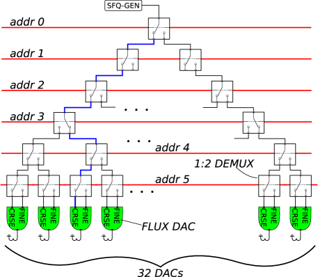
The first of these is a SFQ demultiplexer used as an addressing system. It is constructed as a binary tree of 1:2 SFQ demultiplexer gates as shown in Fig. 1. For the specific design discussed here, the number of address lines is 6. This demultiplexer allows many devices to be addressed using only a few address lines.
The second part is a set of digital-to-analog converters (DACs), located at the leaves of the address tree. These DACs comprise storage inductors that can hold an integer number of single magnetic flux quanta . Their digital input are single flux quanta, and their analog output are the stored flux, which can be coupled into a target device. The magnitude of this output flux is proportional to the number of stored flux quanta. Each DAC has two such storage inductors, a COARSE stage, and a FINE stage, named for the relative strength with which their output flux is coupled to the target device. In our architecture, the output of these DACs is static.
The third part is a method for converting the static output of a DAC to a time-dependent signal. This is achieved by coupling the output of the DAC into a variable gain element, equivalent to the tunable coupler described elsewhere Harris et al. (2009). An analog line carrying a time-dependent current is coupled to the target device via the variable gain element. This approach is useful in the types of circuits of interest here because single analog lines can be shared among large numbers of devices that need the same functional dependence on time, but may require individual tunability of the gain and offset.
We designed, fabricated, and operated integrated circuits comprising this type of control system architecture. One such circuit includes eight superconducting rf-SQUID flux qubits as described in Harris et al. . Though not discussed here, the state of each qubit was read out via a Quantum Flux Parametron (QFP) latch or buffer which was in turn read by an x-y addressible dc-SQUID array as discussed in detail in Berkley et al. . Each rf-SQUID flux qubit has inductive ports coupled to five different DACs, and 24 compound Josephson junction (CJJ) rf-SQUID couplers Harris et al. (2009), each of which is coupled to a single DAC. Thus, this circuit required DACs. The particular control circuit described here comprises two 1:32 demultiplexers with six shared address lines and two separate power lines. This circuit included 1,538 junctions ranging in size from a minimum of 0.6 m diameter (32 of them) to a maximum of 4 m in diameter.
The paper is organized as follows: Requirements on control circuitry derived from the devices, architecture and operating procedures in superconducting adiabatic quantum optimization systems are discussed in section II. The specific control circuitry architecture is discussed in section III. Data demonstrating the performance relative to requirements is presented in section IV. Conclusions are presented in section V.
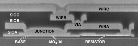
The measurements reported in section IV were performed on chips fabricated in a four Nb layer superconducting process employing a standard Nb/AlOx/Nb trilayer, a TiPt resistor layer, and planarized PECVD SiO2 dielectric layers. Design rules included 0.25 lines and spaces for wiring layers and a minimum junction diameter of 0.6 . A sample process cross section is shown in Fig. 2.
II Magnetic Memory Requirements
Our intent is to embody a specific quantum algorithm in hardware. This algorithm, known as adiabatic quantum optimization (AQO), is a novel approach for solving combinatorial optimization problemsFarhi et al. (2001); Steffen et al. (2003). Unlike the incumbent techniques for such problems, such as simulated annealing or genetic algorithms, AQO algorithms include procedures that are explicitly quantum mechanical. The requirement to provide the quantum mechanical resources necessary for running this algorithm places unusual constraints on processor systems and components.
Quantum computation intimately ties the physics of the underlying hardware to its intended algorithmic use. Both the problem to be solved, and the algorithm used to solve it, are implemented by manipulating the system Hamiltonian. Primarily motivated by this observation, the approach we have taken to design hardware is a top-down one. For the circuits considered here, the requirements are driven by what is required to run the AQO algorithm. To provide context for the material in this section we first provide an overview of the algorithm itself.
Consider the following discrete optimization problem: Given a vector and upper diagonal matrix , where the elements of both are real numbers, find the set that minimizes the objective function
| (1) |
where , and is an set of pairs where is allowed to be non-zero. We call the allowed edge set. The necessity for explicitly defining the set arises because ultimately we will connect this term in the objective function to physical couplings between pairs of qubits, and for a variety of reasons the number of elements in will generally be much less than the total number of possible pairs . A design constraint on processor architecture is that qubits must be connected in such a way so that finding the minimum of Eq. (1) is NP-hard. Even with this constraint, it is straightforward to find realizable sets for which this holds, and we will focus exclusively on these cases.
An AQO algorithm exists for solving this problem. The approach is outlined in Algs. 1 and 2. The control system reported on here enters into these in the load step of Alg. 1.
II.1 Processor Interconnect Architecture
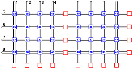
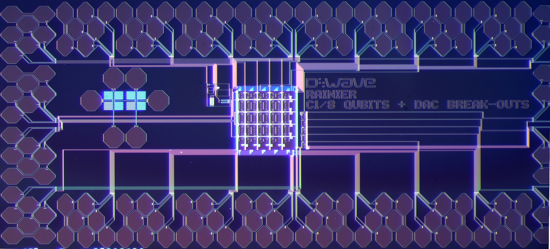
There are many possibilities for how one might try to build a hardware system capable of running Algs. 1 and 2. Here we focus on a unit cell consisting of eight qubits and 24 couplers. See Fig. 3 for a schematic and photograph showing the interconnect pattern. Copies of this unit cell can be connected together, as indicated in the top of Fig. 3, and this is how we design larger systems. This choice of unit cell fixes the allowed edge set , and satisfies the constraint that minimizing Eq. 1 be NP-hard.
II.2 Number of DACs
The total number of DACs required for circuits of increasing complexity is shown in Table 1. Here we provide a brief overview of how these numbers arise, and refer the reader to Harris et al. (2009, ) for further details.
| Unit Cells | Qubits | Couplers | DACS | JJs |
|---|---|---|---|---|
| 1 | 8 | 16 | 56 | 1500 |
| 4 | 32 | 72 | 232 | 6000 |
| 16 | 128 | 328 | 968 | 24000 |
| 64 | 512 | 1416 | 3976 | 96000 |
| 256 | 2048 | 5896 | 16136 | 384000 |
II.2.1 One DAC per Coupler
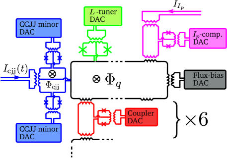
A tunable compound Josephson junction rf-SQUID coupler inductively coupled to qubits and is used to set each desired value of Harris et al. (2009). One such physical device is required per element of the allowed edge set . Couplers are controlled using a static dc flux bias applied to their compound-junction–no time dependence in this signal is required. For this design, the flux bias is provided by the DAC shown in red in Fig. 4.
II.2.2 Five DACs per Qubit
The potential energy of an ideal compound Josephson junction rf-SQUID qubit is Han et al. (1989)
| (2) | |||||
where is the sum of Josephson critical currents in the compound junction, and are the inductance in the qubit and compound-junction loop, respectively. Likewise , , and , are the internal and applied flux for the qubit and CJJ loop respectively.
Eq. 2 is only applicable when the two junctions making up the compound-junction are identical. Junction critical current s of identically drawn Josephson junctions in superconductor fabrication processes are reported to have a normal distribution with a standard deviation of anywhere from 1% to 5% Abelson et al. (1995); Nakada et al. (2003). Thus, we expect real compound-junctions to be naturally imbalanced. This causes difficulties in running the annealing algorithm Alg. 2 Harris et al. . To overcome the junction imbalance problem we use a more complex structure which we call a compound-compound-Josephson junction (CCJJ) which is described in detail in Harris et al. . This provides two additional degrees of control freedom per qubit, which can be used to correct for reasonable junction imbalance ( 5% difference). We access these structures via the blue CCJJ minor DACs in Fig. 4.
As inter-qubit coupling strength is adjusted, the susceptibility of the coupler, and the extent to which it inductively loads the qubit, will change Harris et al. (2009). This causes the qubit inductance in Eq. 2 to be dependent upon the choice of . To overcome the resulting problem-dependent inter-qubit imbalance, we add an additional compound-junction, comprising much larger junctions, in series with the qubit inductance. We call this structure an -tuner Harris et al. . The Josephson inductance of this compound-junction is modified with application of a flux bias applied through an on-chip flux DAC, shown in green in Fig. 4.
As discussed in Harris et al. , care must be taken during annealing to ensure that the final Hamiltonian , the one encoding the problem we wish to solve, is that which was intended. Using a compound-junction to modify the relative weights of and causes and to change during annealing, both in an absolute sense, and relative to each other. This arises because although energy scales and are both functions of the persistent currents in the qubits (), they have different functional dependencies. Qubit changes during annealing, distorting .
To keep the relative scale constant, the value of the applied flux used to implement must change during annealing, but will be different for each qubit, depending on the intended value of for that problem. This is accomplished by giving each qubit another tunable coupler, coupled to both the qubit and a shared external analog flux bias line. We call this an -compensator. Each such coupler is used as a variable gain element, programmed with its own DAC (the pink DAC in Fig. 4), and used to scale a global controlled signal to the locally required .
Finally, each qubit has a DAC that can apply a small dc flux bias to its main loop (the black DAC in Fig. 4).
II.3 Precision and Range Requirements
| Max # | COARSE/FINE | ||||
|---|---|---|---|---|---|
| DAC Type | Span | min | COARSE | FINE | Ratio |
| Qubit Flux | 17 | 17 | 14.1 | ||
| CJJ Balance | 17 | 17 | 14.1 | ||
| L-Tuner | 40 | 10 | 10.7 | ||
| Coupler | 40 | 10 | 10.6 | ||
Requirements on precision and range of flux from the DACs ultimately depend on the precision to which the elements of and are to be specified. The system described here was designed to be able to attain four effective bits of precision on parameters and ; in other words, the elements and can be specified with a relative precision of about 5%. This does not mean that the DACs need only four bits of precision. The DAC requirements are derived from those on Hamiltonian parameters and , based on which aspect of a qubit or coupler is being controlled. In our case, requiring four bits of precision in and typically translates into a requirement of about eight bits of precision in each of the DACs.
The primary design parameters for each DAC is its dynamic range: how much flux is it necessary for the DAC to provide, and how fine a control of that flux is needed. All of the DACs were designed to cover their respective ranges in subdivisions of either 300 or 400 steps. However, they differ in the total amount of flux coupled at maximum range from around 25 for the qubit flux bias DAC to as much as 0.9 from the coupler DAC. A summary of desired flux ranges and minimal flux steps is shown in Table 2.
II.4 Programming Constraints
In the design discussed here, there are five DACs per qubit and one per coupler that need to be programmed to implement a specific problem instance. While the DACs are being programmed, power is applied to the SFQ circuits in the address tree, and the chip will heat. The amount of time we must wait for it to cool afterwards (step 3 in Alg. 1) depends on the peak temperatures reached by the various portions of the circuitry, and the relaxation mechanisms enabling their return to equilibrium Savin et al. (2006). Minimizing overall programming time, including that required to cool, is an important design constraint, and must be considered when comparing control circuitry architectures.
Given the block architecture described above, the number of DACs we must program increases with processor size as shown in Table 1. While not every DAC will need to be programmed for each unique configuration of and in practice, in what follows the assumption will be that all are. In our multiple flux quantum based encoding scheme, the programming time will depend on the value programmed. To estimate the basic scaling with number of devices, it is probably reasonable to assume that each time the processor is programmed for a new problem, each DAC stage must receive on average half of its designed capacity in pulses. For example, the coupler DAC would receive about , the qubit flux bias DAC about , or roughly 20 per DAC in either case.
Programming speed can then be bought at the expense of additional input lines and more parallelization - using more, shallower address trees each with its own separate input.
However, with or without parallelization, one must be able to load all the pulses without errors. The more DACs being programmed, the more pulses there are that must be routed through the address tree with fidelity, and the smaller the acceptable error probability per pulse. For example, per Table 1, with qubits, we require 16,136 DACs. An average problem would require loading flux quanta onto the chip. If we want 95% confidence that we can program problems correctly 99 times out of 100, the probability that any flux quanta makes an error should not be greater than . With 128 qubits, is sufficient.
Bit error probability in SFQ circuits has been extensively studied Herr and Feldman (1996); Q. P. Herr (1999); Satchell (1999). Satisfying these and even more demanding error rate requirements at sub-Kelvin temperatures is straightforward, but needs to be confirmed for any particular implementation.
III Magnetic Memory Architecture
III.1 Two Stage Multiple Flux Quantum DAC with Reset
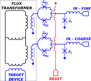
The DACs each have two stages. Each stage comprises a large storage inductor in series with a two-junction reset SQUID, and an input junction, as shown in Fig. 5(a). Each stage was designed with in the range 75 to 300, depending on their function, and thus able to hold in the range of 10 to 40 flux quanta of either polarity. Here L is the stage inductance, and is the effective critical current of the two junction reset SQUID.
 |
 |
|
| (a) | (b) |
The two-junction reset SQUID is used to empty the DAC stage of stored flux. This is accomplished by applying flux to the reset loop, so that its effective critical current , and thus DAC stage , is diminished to below the level required to store flux. For this reset function to be effective, it must be possible to suppress the effective critical current of the reset SQUID to less than that required to store one in the storage inductor. This requirement places an upper bound on the DAC stage . It also places a requirement on how closely matched the s of the two junctions in the reset SQUID must be to each other. This is because the minimum effective critical current will not be less than the difference in the s of the two reset junctions. Thus given a particular fabrication process, with its feature size, penetration depths, and characteristic junction spread, there will be some maximum number of that can be stored in a DAC that can be reliably reset to an empty state. This limits the dynamic range of an individual DAC stage.
| Fine | Coarse | Target | |
|---|---|---|---|
| Fine | |||
| Coarse | |||
| Target |
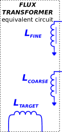
We can achieve a dynamic range greater than that of an individual DAC stage, and shorten programming times, by connecting two or more stages together, as indicated in Fig. 5(a). The intervening transformer couples the different stages into the target circuit with different weights. The flux transformer can be thought of as playing the role of an R-2R ladder, such as is frequently used in construction of semiconductor DACs. One important difference is that successive stages of this DAC differ from each other not by factors of two, but more typically by a factor of ten, depending on the requirements set by the target device. The other difference is that we are transforming and dividing flux rather than voltage.
The flux transformer can be modeled with the equivalent circuit shown in Fig. 5(b), where we consider only two storage inductors , , and the target inductor . The inductance matrix for the equivalent circuit shown in Fig. 5(b) was calculated by modeling the layout using FastHenry 3.0wr wrc , and is shown in Table 3.
The flux coupled out of this DAC can be summarized by the expression:
| (3) |
where represent the integer number of flux quanta that are stored within the respective DAC stages, the coupling constant describing the amount of flux from the COARSE stage into the output device, and , the division ratio between COARSE and FINE, which is typically 10 for the devices discussed here.
III.2 DAC Noise
One concern with using SFQ circuitry in this way arises from the fact that its Josephson Junctions are usually critically damped with external shunt resistors. These resistors are a source of fluctuations which may ultimately decrease the precision with which Hamiltonian parameters and can be specified. In the design presented in Figure 5(a), a number of factors serve to isolate the resistors in the SFQ circuitry from the junctions in the qubit, so that their impact on the qubit can be quite small.
To see this more clearly, we consider a simple lumped element circuit model of the DAC and qubit. A description of our system using lumped elements is reasonable at low enough frequencies, but will eventually fail at higher frequencies, for example when the 1 millimeter long coils in the DAC spirals approach at around 100 gigahertz. Fortunately, we are most concerned with fluctuations occuring at an energy scale comparable to, or less than, the tunnel splitting of our qubits during the annealing algorithm, typically a few gigahertz or lessHarris et al. .
There are many shunted junctions in the SFQ circuits discussed here, but none couples more strongly into the qubit than the input junctions of the various COARSE DAC stages, labelled in Figure 5(a). In what follows, the effect of this junction’s shunt resistor on a qubit is considered by analyzing an equivalent circuit shown in Figure 6(a) for the case of the qubit flux bias DAC. Here the DAC input junction has been linearized, and is represented by its Josephson inductance and junction capacitance . Two different operating points of the DAC input junction, corresponding to the DAC being empty or full of flux, are used to determine the small signal inductance . The qubit’s four CCJJ junctions are represented as a single linearized junction described by and .

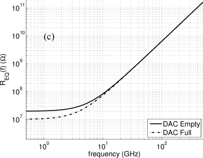
One way to characterize the extent to which fluctuations in couple into qubit junctions is by comparing its effect to that of an equivalent shunt resistor connected directly across the qubit junctions, as indicated in Figure 6(b). The magnitude of will be frequency dependent, and can be determined as where is the admittance of the circuit across the terminals shown in Figure 6(a). The resulting is plotted vs. frequency in Figure 6(c) for circuit parameters described in the caption. At low frequency is around and grows at frequencies above a few gigahertz.
Even at low frequency, most current fluctuations from are shunted by the DAC input junction, whose small-signal inductance is between 100 and 150 times smaller than the DAC storage inductor , depending on the state of the DAC. Noise current that does flow into can in turn couple into the qubit, though it is further reduced by a factor of , or around 1/40 for the circuits discussed here. At higher frequencies fluctuations are further shunted by the junction capacitances.
The other DACs couple into the qubit in a less straightforward fashion, but we can still make a reasonable estimate of their impact. An example is the case of the L-Tuner DAC. The L-Tuner is a dc-SQUID connected in series with the qubit inductorHarris et al. . It is flux biased in such a manner that it would not apply any flux into the qubit if its two , diameter junctions were identical, but does so when they differ. A 1% mismatch between junction critical currents is typical for junctions of this size in our process. A typical operating point for the L-Tuner corresponds to a flux bias of . For this case, following Eq. 4c from Harris et al. , about 1% of the flux applied to the L-Tuner will get applied into the qubit body. This is comparable but smaller than the corresponding factor of of 1/40 discussed for the qubit flux bias DAC. For this reason, we expect the corresponding for the case of the L-Tuner DAC to be larger than that of the qubit flux bias DAC. It should then have a relatively smaller effect on the qubit. Similar arguments apply to the other DAC types.
An of will contribute approximately flux noise into the qubit, considerably less than the 1.3 at 1 Hz observed in 1/f noise in our qubits Harris et al. ; Lanting et al. (2009). Thus we do not expect the shunt resistors in our control circuitry will add a significant amount of flux noise to our qubits.
III.3 Programmable time-dependent signals
As discussed in section II.2.2, we require the ability to supply time dependent signals to each of the qubits to compensate for the fact that the qubit persistent current changes during the annealing process. These time dependent signals need to have the same temporal shape but with different magnitudes. The DACs discussed above can hold static flux, and are not suited to provide real-time signals. This is because they do not include a sample-and-hold stage to protect the output from transients during programming. Moreover, real-time updating of the DACs would raise the temperature of the chip to an unacceptable level.
Rather, time dependent signals can be customized using the tunable coupler discussed in Reference Harris et al. (2009) as a variable or programmable gain element. A global analog bias line holding a master copy of the desired time dependent signal is coupled to each qubit on the chip through its own programmable gain element, as indicated in Fig. 7. Each programmable gain element is controlled by its own DAC. In conjunction with an additional DAC (not shown) to provide a flux offset to each target device, the master copy of the signal can be uniquely transformed for each target in the following manner:
| (4) |
where and are programmable on a per device basis. This is not as flexible as having independent arbitrary waveform generators for each device, but it is flexible enough to satisfy the requirements of the compensator.

III.4 Demultiplexer Tree

The DACs discussed above were loaded with SFQ pulses routed through a binary tree demultiplexer circuit shown in Fig. 1. Each address tree is fed SFQ pulses originating in an SFQ generator circuit, namely a flux biased dc-SQUID. Each node of the tree is made of a 1:2 SFQ demultiplexer circuit, as shown in Fig. 8. The 1:2 demultiplexer circuit is addressed with a magnetically coupled flux bias line which steers an incoming SFQ pulse to one of its outputs based on the sign and magnitude of current on that address line.
Reversing the polarity of the bias current allows flux quanta of opposite polarity to be routed, though the sign of the address current must also be reversed to get this negative flux to the same output port. This makes use of a symmetry not commonly exploited in RSFQ circuits. Here it allows the DAC stages to store flux of either sign, and allows the state of each stage to be both incremented and decremented. This in turn allows DAC programming to be performed incrementally - starting from the previously programmed state without first resetting to the empty (no stored flux) state.
Address lines are shared for all demultiplexer nodes at a particular depth of the tree. The final address line in the tree chooses between COARSE and FINE stages of each DAC. The 64 DACs mentioned above are served by two separate trees, each addressing 32 DACs. These trees require five address lines to address a particular DAC, plus a sixth line to choose between FINE and COARSE, giving a total of six address lines to service the circuit block.
IV Demonstration of control circuit functionality
For the circuit block discussed in this paper, the control circuitry in its entirety represents moderate complexity - certainly not the most complex or heterogeneous SFQ circuit demonstrated to date, nor the one with the most junctions. The eight qubit circuit block reported here, including the attached control circuitry, contains just over 1,500 Josephson junctions and 2,000 resistors. Nevertheless, implementation of a new design in a new foundry requires careful performance evaluation. We must determine that the circuit yielded, operated as designed, and whether variances are due to design or fabrication issues. We must determine if it meets its design requirements.
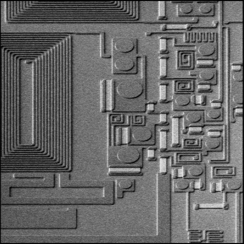
A scanning electron microscope (SEM) image of a portion of one of the DACs and demultiplexer cells equivalent to those reported here is shown in Fig. 9. The image was taken after patterning of the trilayer and subsequent junction definition. Uncontacted junctions appear as circles and are still visible in the demultiplexer circuitry toward the right of the image. Subsequent fabrication involves the deposition of three planarized dielectric layers and three additional metal (Nb) layers. Junctions in this circuit have critical currents in the range . Resistors are also visible and appear as rectangles contacted at each end. Bias resistors are long and thin while shunt resistors for this portion of the circuitry are relatively wide. The coils visible on the left are portions of the two storage inductors for one of the L-Tuner DACs. The coils are patterned with lines and spaces. The DAC’s reset junctions are visible in the upper center of the image. To the right is one of the demultiplexer cells. The entire field of view is approximately in width and top to bottom.
In the architecture described above, many of the DACs are embedded deeply within the circuit, with no convenient or direct method to determine how much flux they actually apply to the target per in the FINE and COARSE stages. This inconvenience is addressed in two ways: Each variant of DAC is implemented in a separate stand-alone or break-out circuit in which it applies a flux bias directly to a two-junction dc-SQUID. The dc-SQUID vs modulation curve is then measured vs. DAC state, and a precise calibration of FINE and COARSE weights ( and ) can be extracted. Data from parameters extracted in this way is presented in Table 4. Second, within the body of the circuit block, wherever a DAC is used to apply a flux bias, an analog line is also used to flux bias that target device in parallel with that DAC. This combination is indicated in the inset of Fig. 10. This single analog line is shared amongst all like control nodes for all qubits, so that only a handful of such lines are required to service the entire chip. Of course, the shared analog line cannot be used for independent control of all devices simultaneously, but it is nevertheless useful for testing individual devices. For example, each qubit is flux biased by its own DAC and a single shared externally accessible analog line. The qubit degeneracy point is easily measured Berkley et al. . If the DAC is then programmed with, for example, in its COARSE stage, one can determine the change in current on that analog qubit flux bias line required to compensate for the shift in degeneracy point. This allows us to find the ratio of mutual inductance between the analog line and the qubit to that between each DAC stage (COARSE & FINE) and the qubit. We can independently measure the mutual inductance of the analog line into the qubit by noting the periodicity in its response. We can then determine and for that DAC, which are the parameters we need to determine how much flux the DAC applies to its target.
This feedback measurement is applicable to determining and for DACs used for various types of control, not just qubit flux bias. The only thing that differs is the nature of the measured quantity. For the qubit flux bias DAC, the qubit degeneracy point is used. For the L-Tuner DAC, a measure of the qubit’s inductance, ultimately a measure of its circulating current, can be used. For the CCJJ DACs, a measure that quantifies the imbalance in the qubit’s compound-junction is used. In all cases we use the measured quantity to determine what analog signal is necessary to compensate for a change in the programmed DAC state. In this way we can determine how much flux each DAC on chip applies to its target.
IV.1 DAC Biasing a dc-SQUID
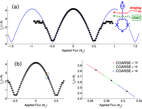
The couplers shown in red in Fig. 3 are designed to couple qubits between different unit cells. For the eight qubit unit cell under study here, these were not connected to qubits on both ends. Instead, the inter-unit cell couplers were wired up in such a way that their compound-junction, still biased by its own DAC, could be operated as a hysteretic dc-SQUID. This coupler’s DAC could thus be used to apply flux to a dc-SQUID, and so we traced out the vs threshold characteristics for this dc-SQUID as discussed in Reference Berkley et al. . The vs curve shown in Fig. 10 was taken both with an analog flux bias controlled directly from room temperature electronics ((a), blue dots) or using the DAC ((a), black circles). To make such a plot, we have to know the coupling constant between the COARSE DAC stage and the dc-SQUID it biases, as well as the mutual inductance between the analog bias line and the dc-SQUID. As mentioned earlier, the mutual inductance between analog line and dc-SQUID is easily determined by observing the periodicity of the modulation curve. Also discussed earlier, the coupling constant and division ratio are measured separately with a feedback procedure.
The two threshold curves shown in Fig. 10a begin to deviate from each other past about . This corresponds to where the COARSE stage of this DAC has reached its capacity, and fails to store additional flux. To be clear, the black circles are plotted vs. flux programmed into the DAC COARSE stage, not flux actually applied by that DAC stage to the dc-SQUID. A plot of the latter would fall on top of the blue dots.
Fig. 10b shows the same threshold curve vs. flux programmed into the COARSE stage (black dots), but in addition, at COARSE values of , , and , flux ranging from to is programmed into the FINE DAC stage as well. This is shown in the boxed region in Fig. 10b, which in turn is expanded in Fig. 10c. In Fig. 10c, it is clear that there is sufficient range in the FINE DAC stage to bridge the COARSE DAC steps.
It is worth noticing that the range of the FINE DAC achieved from adjacent COARSE settings overlap each other. It is essential that they do not underlap, as this would result in holes in the range of flux that could be provided by the DAC. This means that there can be more than one way to obtain a particular output FLUX. But while the ranges overlap, the specific levels achieved from adjacent COARSE settings do not, in general, line up. Of course there is no need for them to.
To use the DAC, it is necessary for the reset function to operate. A reset operation is made by first increasing the flux bias on the reset SQUID (shown in Fig. 5) to a predetermined level, and then lowering it back to zero. The predetermined level is chosen to be just beyond the current corresponding to a flux bias of on the reset SQUID. This reset pulse was usually adequate to reset the DAC. There were cases when the s of reset junctions for a particular DAC stage differed from each other by more than about 5%, where a single reset pulse was not sufficient, and the DAC could retain one or two after the reset. In these cases, the reset pulse had to be repeated several times to consistently empty the DAC. While the correlation between junction spread, DAC stage , and reset function is not quantitatively understood by us, we expect the problem to worsen with increased junction spread, and with increased DAC stage storage capacity (). We found that for the chips reported upon here, it was always possible to reset all of the DAC stages by applying multiple reset pulses.
IV.2 DAC applying flux bias to a qubit
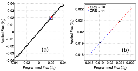
Each qubit has a DAC that can apply a flux bias to its body. Fig. 11 shows the flux response relative to the COARSE and FINE stages for one of these DACs. The limits of the COARSE stage capacity are just visible at the extrema of the plot. To adequately cover the range, the maximum span achievable with the FINE stage must be enough to cover one step of the COARSE stage. This coverage is clearly attained in Fig. 11.
IV.3 DAC control of inter-qubit coupling
One of the most challenging cases to treat in the design of these DACs was the situation in which a large flux span needed to be applied to a low inductance SQUID. This situation is most extreme in the case of the coupler DAC and the -tuner DAC. In fact, the dc-SQUID threshold curve presented in Fig. 10 above is an example of such a case - these dc-SQUIDs are patterned identically to the compound-junction used in the coupler and -compensator.
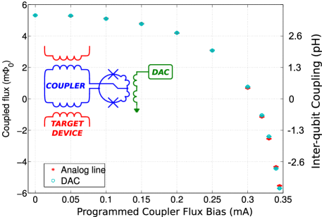
We can also observe a DAC controlling inter-qubit coupling. Fig. 12 shows a plot of the effective coupling between two qubits, via a tunable coupler, as a function of flux applied to control the coupler by an analog control line (red points). Inter-qubit coupling using the DAC to control the same coupler is shown as blue circles in the same plot. More details about the type of measurement used to obtain this plot are discussed in Harris et al. (2009).
While presented as an inter-qubit coupler, a similar device is employed in customizing shared time-dependent signals, as discussed in section III.3. The key difference is that in Fig. 7, one of the qubit ports on the coupler is connected to a global analog bias line. We found it straightforward to operating this programmable coupler in the fashion described in section III.3.
IV.4 Summary of DAC performance
| COARSE Step | FINE Step | |||
|---|---|---|---|---|
| DAC Type | Design | Achieved | Design | Achieved |
| Qubit Flux | ||||
| CCJJ | ||||
| L-Tuner | ||||
| Coupler | ||||
| MAX COARSE | Max Coupled Flux | |||
|---|---|---|---|---|
| DAC Type | Designed | Achieved | Designed | Achieved |
| Qubit Flux | 17 | 22 | 0.050 | 0.077 |
| CCJJ | 17 | 22 | 0.093 | 0.086 |
| L-Tuner | 41 | 40 | 0.460 | 0.339 |
| Coupler | 41 | 35 | 0.960 | 0.665 |
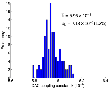
Table 4(a) summarizes design targets vs. achieved COARSE and FINE step sizes for the various types of DAC implemented on the eight-qubit block. Data from Table 4(a) are extracted from separate break-out versions of the circuit. Uncertainties reported derive from the measurement uncertainty of that parameter for that individual device. Measuring these parameters in-situ using the feedback technique described above shows device-to-device variation with a standard deviation of typically 2%. For example, the distribution of values measured for qubit flux bias DACs on a chip containing a 4x4 array of tiled unit cells, shown in Fig. 13, exhibits a relative standard deviation of 1.2%. This is consistent with observed variation in mutual inductance of simple microstrip transformers used in this circuit, such as might occur with variations in dielectric thickness of the same scale. Table 4(b) summarizes the maximum number of SFQ and maximum coupled flux by each DAC type.
It is worth observing that we were able to confirm that all 64 of the two stage DACs on the single-unit-cell eight-qubit chips discussed here yielded. By yielded we mean that they behaved as expected, per Tables 4(a) and 4(b), and that variations in coupling between identically designed DACs were of the order of 2%. Moreover, there were no significant differences in maximum storage capacity between identically designed copies. This strongly suggests that the DAC storage coils yielded. An inter- or intra-layer short in one of the coils would likely have changed that coil’s storage capacity significantly, and this would have been observable.
Deviations between design targets and achieved parameters for this chip are as large as 30% for some of the couplings. This is primarily due to the challenge of performing sufficiently accurate 3D electromagnetic modeling of the superconducting inductors and transformers used in creating the two-stage DACs.
IV.5 Demonstration of Demultiplexer Functionality
Delivering pulses to the DAC requires that bias current and address signals be applied to the demultiplexer tree. Bias current is shared for all demultiplexer circuits in a particular tree, and address is common for all demultiplexers at a particular level in the tree. The design and fabrication of the chip must be sufficiently uniform such that all cells work with common levels. It is also necessary that the operating margins are wide enough that a robust, low error rate operating point can be obtained.
As discussed in section IV.1, several DACs that are attached to unused boundary couplers are wired up for use as dc-SQUIDs. Operating margins required to address the FINE and COARSE DAC stages of each of these were obtained with respect to global bias current and level of address signal. These operating regions are shown in Fig. 14. Routing an SFQ pulse to a particular DAC requires the successful navigation of six demultiplexer gates, each with its own address current. While the signs of these various address levels may differ, their magnitude in flux was held to a common value, and this common magnitude of address flux is the address axis in Fig. 14.
As far as addressing these six DACs, there is clearly adequate uniformity in this demultiplexer tree that they can all be operated at a common bias current and address level. We have determined that all 64 DACs on the chip discussed here, as well as those on another subsequently tested, were addressable with chip-wide common bias current and address levels.
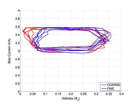
Fig. 14 shows the boundary outside of which the probability of failing to increment a DAC stage is of order 0.1 or higher. As mentioned in section II, we require the error rate to be considerably less than this. The dependence of error probability in SFQ circuits has been studied in some detail by a few different groups Herr and Feldman (1996); Q. P. Herr (1999); Satchell (1999). However, we are interested in the aggregate error probability of the entire demultiplexer tree. The probability that a pulse fails to be loaded into a DAC was measured as a function of demultiplexer bias current at nominal address level, and is shown in Fig. 15.
As expected, the margins decrease as the error probability requirement decreases. There is a significant bias current range with . At the chosen operating point, over 15,000,000 operations were performed, and no errors were observed. This places an upper bound on the probability of error with 95% confidence.
It is not sufficient that the address tree route pulses to the addressed DAC. It must do so exclusively, and not route pulses to any other DAC. Confirming that pulses arrived at the intended location, a requirement to attain the data shown above, does not demonstrate exclusivity.
Indeed if significantly overbiased, with no address applied, the demultiplexer tree is capable of operating in a broadcast mode, where pulses are duplicated rather than routed at each 1:2 demultiplexer node. While this should not happen under normal circumstances, failure to test for this would be an oversight.
Testing exclusivity was performed for most of the DACs on one of the chips tested at nominal bias current and address levels by (1) confirming that a DAC was addressable and could be programmed, and then (2) sending pulses to every other DAC on that tree and confirming afterward that the state of was unchanged. No cases of pulse misdirection were observed.

V Conclusion
We have presented a description of a functioning system of on-chip programmable magnetic memory designed to manipulate the parameters and state of rf-SQUID superconducting qubits for use in implementing AQO algorithms. The system is inherently scalable, and in turn allows specialized AQO hardware to be scaled to very large numbers of devices.
Based on classical manipulation of single quanta of magnetic flux, the system was implemented in a planarized four superconductor metal layer process with minimum junction diameter and lines and spaces for wiring. The control system was fabricated on-chip, in the same process as the qubits and inter-qubit couplers.
Both the two-stage flux DACs used to manipulate the various controls on the qubits, and the demultiplexer address tree used to address those DACs were shown to work as intended. The address tree is shown to pass SFQ pulses with very low error rate, and to address the DACs exclusively. The two-stage DAC design was shown to be effective at providing a flux bias with a dynamic range in excess of eight bits of precision (at dc). The design targets on several variants of DAC were presented, and while the variations between designed and achieved flux coupled into target sometimes reached 30%, this is close enough to satisfy our current requirements.
While the control system described here was designed to operate an AQO processor, it is probable that the devices described - programmable flux DAC, programmable variable gain element, SFQ demultiplexer tree - can be used to control other types of quantum information processors implemented with superconductors.
References
- (1) W.M. Kaminsky, S. Lloyd, and T.P. Orlando, “Scalable superconducting architecture for adiabatic quantum computation,” quant-ph/0403090v2 .
- Likharev and Semenov (1991) K. K. Likharev and V. K. Semenov, “RSFQ logic/memory family: a new Josephson junction technology for sub-teraherz clock frequency digital systems,” IEEE Trans. Appl. Supercond., 1, 3–28 (1991).
- Hurrell et al. (1980) J.P. Hurrell, D. C. Pridmore Brown, and A. Silver, “Analog-to-digital conversion with unlatched squid’s,” IEEE Trans. on Elec. Dev., 27, 1887–1896 (1980).
- Abelson and Kerber (2004) L.A. Abelson and G.L. Kerber, “Superconductor integrated circuit fabrication technology,” Proc. IEEE, 92, 1517–1533 (2004).
- Silver et al. (2003) A Silver, A Kleinsasser, G Kerber, Q Herr, M Dorojevets, P Bunyk, and L Abelson, “Development of superconductor electronics technology for high-end computing,” Superconductor Science and Technology, 16, 1368 (2003).
- (6) www.hypres.com/pages/foundry/bfoundnio.htm .
- Castellano et al. (2007) Maria Gabriella Castellano, Fabio Chiarello, Roberto Leoni, Guido Torrioli, Pasquale Carelli, Carlo Cosmelli, Marat Khabipov, Alexander B Zorin, and Dmitri Balashov, “Rapid single-flux quantum control of the energy potential in a double squid qubit circuit,” Superconductor Science and Technology, 20, 500–505 (2007).
- Xingxiang et al. (2001) Z. Xingxiang, J. L. Habif, A. M. Herr, M. J. Feldman, , and M. F. Bocko, “A tipping pulse scheme for a rf-squid qubit,” IEEE Trans. Appl. Supercond., 11, 1018–1021 (2001).
- de Castro et al. (2001) R. C. R. de Castro, M. F. Bocko, A. M. Herr, C. A. Mancini, , and M. J. Feldman, “Design of an rsfq control circuit to observe mqc on an rf-squid,” IEEE Trans. Appl. Supercond., 11, 1014–1017 (2001).
- Orlando et al. (2002) T. P. Orlando, S. Lloyd, L. S. Levitov, K. K. Berggren, M. J. Feldman, M. F. Bocko, J. E. Mooij, C. J. P. Harmans, and C. H. van der Wal, “Flux-based superconducting qubits for quantum computation,” Physica C: Superconductivity, 372–376, 194–200 (2002).
- Semenov and Averin (2003) V. K. Semenov and D. V. Averin, “Sfq control circuits for josephson junction qubits,” IEEE Trans. Appl. Supercond., 13, 960–965 (2003).
- Berggren (2004) Karl K. Berggren, “Quantum computing with superconductors,” Proceedings of the IEEE, 92, 1630–1638 (2004).
- Kaplunenko and Ustinov (2004) V.K. Kaplunenko and A.V. Ustinov, “Experimental test of a superconducting digital interface for vortex qubits,” Eur. Phys. J. B, 38, 3–8 (2004).
- Harris et al. (2009) R. Harris, T. Lanting, A. J. Berkley, J. Johansson, M. W. Johnson, P. Bunyk, E. Ladizinsky, N. Ladizinsky, T. Oh, and S. Han, “Compound josephson-junction coupler for flux qubits with minimal crosstalk,” Phys. Rev. B, 80, 052506 (2009).
- (15) R. Harris, J. Johansson, A.J. Berkley, M.W. Johnson, T. Lanting, Siyuan Han, P. Bunyk, E. Ladizinsky, T. Oh, I. Perminov, E. Tolkacheva, S. Uchaikin, E. Chapple, C. Enderud, C. Rich, M. Thom, J. Wang, B. Wilson, and G. Rose, “Experimental demonstration of a robust and scalable flux qubit,” To Be Published in Phys. Rev. B (a), arXiv:0909.4321v1 .
- (16) A. J. Berkley, M. W. Johnson, P. Bunyk, R. Harris, J. Johansson, T. Lanting, E. Ladizinsky, E. Tolkacheva, M. H. S. Amin, and G. Rose, “A scalable readout system for a superconducting adiabatic quantum optimization system,” arXiv:0905.0891v1 .
- Farhi et al. (2001) Edward Farhi, Jeffrey Goldstone, Sam Gutmann, Joshua Lapan, Andrew Lundgren, and Daniel Preda, “A quantum adiabatic evolution algorithm applied to random instances of an np-complete problem,” Science, 292, 472–475 (2001).
- Steffen et al. (2003) Matthias Steffen, Wim van Dam, Tad Hogg, Greg Breyta, and Isaac Chuang, “Experimental implementation of an adiabatic quantum optimization algorithm,” Phys. Rev. Lett., 90, 067903 (2003).
- Han et al. (1989) S. Han, J. Lapointe, and J. E. Lukens, “Thermal activation in a two-dimensional potential,” Phys. Rev. Lett., 63, 1712–1715 (1989).
- Abelson et al. (1995) L.A. Abelson, N. Martinez K. Daly, and A.D. Smith, “Lts josephson junction critical current uniformities for fine applications,” IEEE Trans. Appl. Supercond., 5, 2727–2730 (1995).
- Nakada et al. (2003) D. Nakada, K.K. Berggren, E. Macedo, V. Liberman, and T.P. Orlando, “Improved critical-current-density uniformity by using anodization,” IEEE Trans. Appl. Supercond., 13, 111–114 (2003).
- (22) R. Harris, A. J. Berkley, J. Johansson, M. W. Johnson, T. Lanting, P. Bunyk, E. Tolkacheva, E. Ladizinsky, B. Bumble, A. Fung, A. Kaul, A. Kleinsasser, and S. Han, “Implementation of a quantum annealing algorithm using a superconducting circuit,” (b), arXiv:0903.3906v1 .
- Savin et al. (2006) A. M. Savin, J. P. Pekola, D. V. Averin, and V. K. Semenov, “Thermal budget of superconducting digital circuits at subkelvin temperatures,” Journal of Applied Physics, 99, 084501 (2006).
- Herr and Feldman (1996) Quentin P. Herr and Marc J. Feldman, “Error rate of a superconducting circuit,” Applied Physics Letters, 69, 694–695 (1996).
- Q. P. Herr (1999) M. J. Feldman Q. P. Herr, M. W. Johnson, “Temperature-dependent bit-error rate of a clocked superconducting digital circuit,” IEEE Trans. Appl. Supercond., 9, 3594–3597 (1999).
- Satchell (1999) J. Satchell, “Limitations on hts single flux quantum logic,” IEEE Trans. Appl. Supercond., 9, 3841–3844 (1999).
- (27) www.wrcad.com/ftp/pub/README.FASTHENRY .
- Lanting et al. (2009) T. Lanting, A. J. Berkley, B. Bumble, P. Bunyk, A. Fung, J. Johansson, A. Kaul, A. Kleinsasser, E. Ladizinsky, F. Maibaum, R. Harris, M. W. Johnson, E. Tolkacheva, and M. H. S. Amin, “Geometrical dependence of the low-frequency noise in superconducting flux qubits,” Phys. Rev. B, 79, 060509 (2009).