Photo-Thermoelectric Effect at a Graphene Interface Junction
Abstract
We investigate the optoelectronic response of a graphene interface junction, formed with bilayer and single-layer graphene, by photocurrent (PC) microscopy. We measure the polarity and amplitude of the PC while varying the Fermi level by tuning a gate voltage. These measurements show that the generation of PC is by a photo-thermoelectric effect. The PC displays a factor of 10 increase at the cryogenic temperature as compared to room temperature. Assuming the thermoelectric power has a linear dependence on the temperature, the inferred graphene thermal conductivity from temperature dependent measurements has a dependence below 100 K, which agrees with recent theoretical predictions.
pacs:
78.20.Nv, 73.23.-b, 72.40.w, 73.50.LwWhen a photosensitive device is illuminated by light, an electric current, known as photocurrent (PC), can be generated. PC generation in semiconductor optoelectronic devices is mainly due to separation of the excited electron and hole pair by a built-in electric field, as shown in Fig. 1(a). It is also known that if a temperature gradient is generated by light across an interface between two materials, which have different thermoelectric power (), there is PC generation by the photo-thermoelectric effect (PTE), as shown by Fig. 1(b). The magnitude of the generated PC is directly proportional to , which is also a measure of the partial molar entropy. Since entropy is proportional to the density of states (D(E)), from the second law of thermodynamics, the hot carriers tend to diffuse to the material with larger D(E) to maximize the entropy.
Graphene is an interesting material with unusual electronic, optical, and thermal properties GeimGrapheneFab ; GeimQH ; Chen ; LauNanoletter ; Yzhang ; KimQH . Since the conduction and valence band touch each other at the Dirac point GeimGrapheneFab ; KimQH ; Semenoff , there is no bandgap for graphene. A question naturally arises as to which mechanism dominates the PC generation in graphene optoelectronic devices. There have been a few studies focusing on the room temperature opto-electronic response at the junction formed by single layer graphene and metal contacts GiovannettiPRL ; LeeNatureNano ; AvourisNanoLetter ; ParkNanoletter ; AvourisPRB . The generated PC is interpreted based on the built-in electric field picture. However, recent transport measurements demonstrated the thermoelectric effect in graphene transistor devices KimGrapheneThermal ; LauGraphenePRL , which suggests the PTE may play an important role in PC generation in graphene devices. It is the aim of this paper to elucidate the fundamental physical mechanism giving rise to the opto-electronic response at zero-bandgap graphene heterostructures.
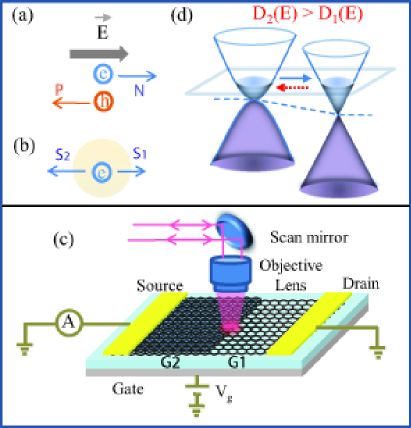
A graphene interface junction, formed by single and bilayer graphene (G1/G2) as shown in Fig. 1(c), will give rise to opposite signs of PC for the two different mechanisms. Thus it provides a unique opportunity to identify the origin of PC. Since single-layer graphene has a linear energy-momentum dispersion relation and bilayer has a quadratic dispersion relation, the D(E) of single-layer () is smaller than that of bilayer ( finite constant) when the Fermi energy () is not far away from the Dirac point. Thus, for the same charge density, of a single-layer is larger than that of the bilayer, i.e. there is a built-in potential difference.
The aligned Fermi level between single and bilayer graphene leads to the Dirac point of the single layer being lower than the bilayer, as shown in Fig. 1(d). According to the electric field picture, the photo-excited electrons would be expected to flow from the bilayer to the single-layer, shown by the blue arrow, and result in a positive PC in the present experimental setup. However, if the PTE is the correct mechanism generating PC, since , the electrons should flow from the single to the bilayer and result in a negative PC, shown by the red dashed arrow. By identifying the sign of the PC experimentally, we can determine which mechanism dominates.
The graphene device is fabricated by mechanical exfoliation of graphite sheets onto a 90nm wafer GeimQH . The single and bilayer graphene are identified by optical contrast and Raman spectroscopy GeimRamanPRL . Au/Cr or Au/Ti electrodes are deposited using photolithographic patterning or shadow mask techniques. The device is held in a vacuum cryostat with a temperature control from 10 to 300 K. The PC and the correlated reflection image are simultaneously obtained by scanning the laser across the device LeeNatureNano ; AvourisNanoLetter ; ParkNanoletter ; AvourisPRB . The laser excitation wavelength is fixed at 635 nm and the laser spot is about 1 . All the PC images presented in this work are taken at zero source-drain bias. We have measured eight different devices and obtained consistent results.
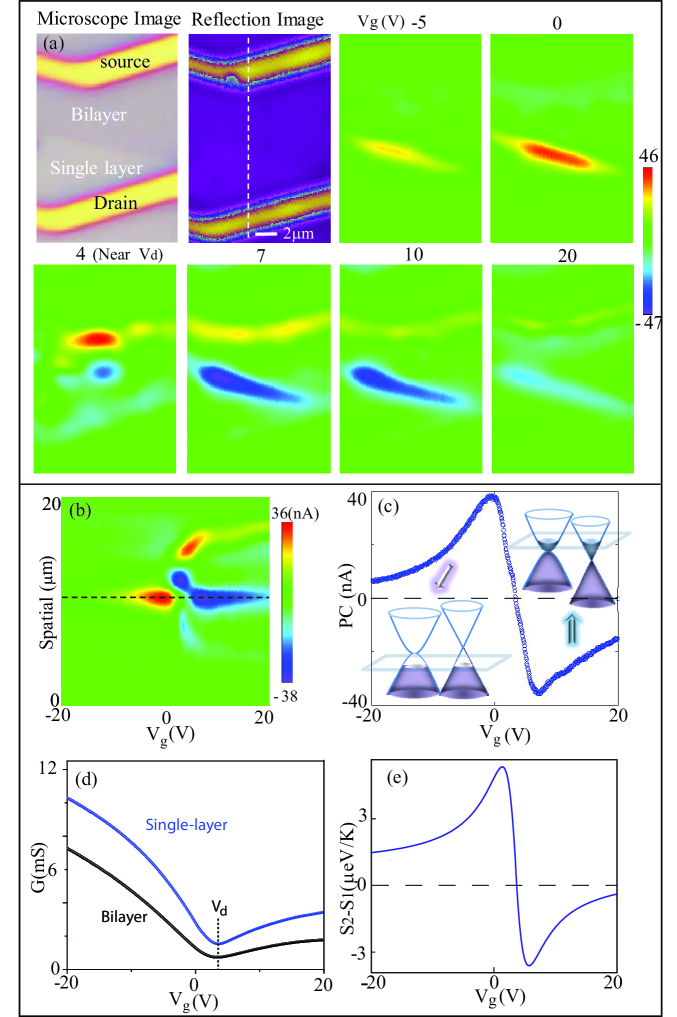
Figure 2(a) displays the PC images of device 1 with the same color scale at various gate voltages () and a temperature of 12 K. Pronounced PC is seen at the graphene-metal contact interface (G/M) and G1/G2. The PC image in Fig. 2(b) is taken by scanning the laser along the dashed white line indicated in the refection image while sweeping the gate voltage continuously. The PC generation at the G/M has been intensively studied and was mainly attributed to carrier separation by the built-in electric field LeeNatureNano ; AvourisNanoLetter ; ParkNanoletter ; AvourisPRB . In the following, we will focus on the optoelectronic response from G1/G2.
By tuning the gate voltage from smaller than to larger than , where corresponds to the Dirac point as shown in Fig. 2(d), the majority carrier in the graphene changes from hole to electron. The PC at G1/G2 switches signs, changing from positive (red) to negative (blue). Figure 2(c) shows the gate voltage dependence of the PC at G1/G2, which is the linecut across the dashed black line in Fig. 2(b). The PC amplitude evolves as the gate voltage varies. On the hole doping side, the PC amplitude increases first, reaches a maximum, and then decreases as the gate voltage increases. The same observation holds for electron doping.
With all the above experimental observations, we determine that the PTE dominates the PC generation at G1/G2, instead of the built-in electric field. Our conclusion is primarily based on the fact that dominance by the built-in electric field would result in positive (negative) PC for the electron (hole) doping, which is clearly opposite to the experimental observations.
The physical picture for PC generation due to the PTE is the following: after the electrons are excited from the valence band to the conduction band, they initially relax back to the Fermi level on the time scale of by phonon emission and form a hot Fermion distribution SundongPRL ; RanaNanoLetter . Since is larger than , the hot free carriers tend to diffuse from the single-layer into the bilayer due to the temperature gradient across G1/G2, which leads to a negative (positive) current for electron (hole) doped graphene.
To make a quantitative comparison between the theory and experiment, the PC generated by the PTE can be formulated as
| (1) |
where is thermoelectric power, is the resistance, and is the temperature difference. From the Mott relation MottPR ; KimGrapheneThermal ; LauGraphenePRL , we have the Seebeck coefficient as
| (2) |
where is the Boltzmann constant, e is electron charge, T is temperature, G is conductance, and is the Fermi energy. The conductance G is proportional to for graphene, where n is charge density and is the electron mobility. When is away from the Dirac point, is approximately a constant and is proportional to D(E).
The calculated as a function of is shown in Fig. 2(e). In the calculation, the term is replaced by , where can be derived from the conductance measurements. The dependence of on the charge density n can be derived from tight binding calculations FermiEnergyvsChargeDensity . For single layer graphene, and is the Fermi velocity. For bilayer, and is the interlayer coupling strength. The calculated qualitatively reproduce the lineshape and sign of the experimental data in Fig. 2(c) note . reverses sign at 3.7V, which is close to the sign switch of PC at 3.4V.
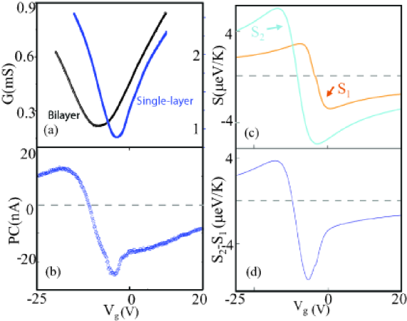
The PTE can account for the experimental results from devices with non-overlapping Dirac points between the single and bilayer. An example (device 2) is shown by the gate dependent conductance measurement in Fig. 3(a), where the bilayer Dirac point is 5V lower than that of the single-layer. The PC at the G1/G2 as a function of is shown in Fig. 3(b). When is between the two Dirac points, i.e. the single-layer is p doped but the bilayer is n doped, of the single-layer has the opposite sign of bilayer, as shown in Fig. 3(c). Thus, the difference in reaches a maximum at a certain between the two Dirac points, which corresponds to a maximum in the PC data. The calculated for device 2, shown in Fig. 3(d), qualitatively reproduces the lineshape and sign of the PC.
We also performed temperature and power dependent studies of PC. We plot the absolute PC amplitude of device 2 at V as a function of temperature in Fig. 4(a). The PC amplitude decreases nonlinearly as the temperature increases. We replot the data on a logarithmic scale in Fig. 4(b), which can be separated into two regions around a temperature of 100 K. The data are fitted with a line with a slope of -0.5 (-1.5) for below (above) 100K. For instance, the PC images of device 2 at 14 K and at 295 K are also displayed on the left and right of Fig. 4(c).
The PTE naturally explains the temperature dependent data. Equation (1) shows that the PC is proportional to , where is the thermal conductivity. Since has an approximate dependence KimGrapheneThermal ; LauGraphenePRL and has a power law dependence of with ThermalConductivity ; TM2 ; Thermal3 ; ThermalC4 , PC is expected to have a nonlinear dependence of , which agrees with the experimental results. Since the slope in Fig. 4(b) corresponds to , we infer that has a () dependence below (above) 100 K.
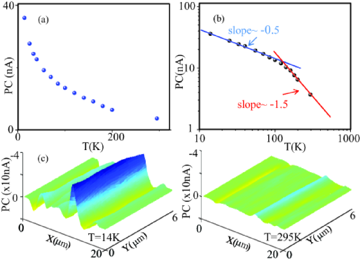
The dependence at high temperature is similar to of the graphite ThermalConductivity . The dependence at low temperature agrees with the recent theoretical prediction of graphene ThermalConductivity ; TM2 ; Thermal3 ; ThermalC4 . It suggests that at low temperature, the out-of-plane acoustic phonon mode, which has a quadratic dispersion relation, contributes to the thermal conductivity. The observation also indicates that the phonon-induced dominates the electron-induced when is close to TM2 .
We can estimate the magnitude of the PC generated by the PTE using Eq. (1) and (2). of single-layer graphene has been reported as at room temperature LauNanoletter . Taking the heat flow as a radial wave, given that , where h is the thickness of graphene of , P is incident laser power of 40 , and is the absorption coefficient of , we infer that is on the order of 0.1K. Taking on the order of by calculation from Eq . (1) and the resistance of graphene on the order of , the PC is on the order of 2 nA, which is consistent with the experimental observations at room temperature.
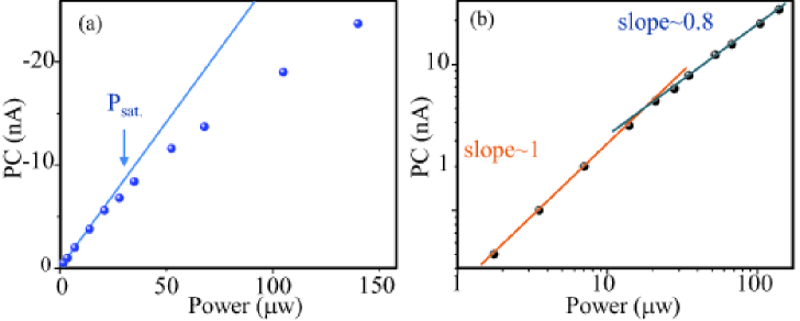
With the knowledge of and as functions of T, we should be able to predict the power dependence of the PC at low temperature. From Eq. (1) and (2), we have . When the laser power is strong enough, the induced temperature difference dominates. Thus, can be approximately taken as , which leads to . On the other hand, from and , we have , which leads to . Taking from the temperature dependent measurement, we expect that the PC should have dependence for strong laser power at low temperature.
The obtained laser-power-dependent PC measurements confirm the above predictions. Taking the PC amplitude as a function of laser power at T=30K as an example, shown in Fig. 5(a), we observe a PC saturation effect. The blue line is a guide to the eye and the PC deviates from the linear dependence around 20 (corresponding to ). The data are replotted on a logarithmic scale in Fig. 5(b). A line fit with a slope of 1 corresponds to the data in the linear region. With strong laser power, the PC shows a dependence, which is in excellent agreement with the prediction from the PTE picture.
A final question is whether the PC at a G/M or the interface P-N junction is also generated by the PTE. We know that is negative for electrons and positive for holes in graphene. For the G/M, the thermal voltage drives electrons (holes) from the metal contact to the graphene for the n (p) doping, which leads to positive (negative) PC at the source and negative (positive) at the drain. The PC reverses polarity as the majority carrier changes from electron to hole. For the P-N junctions formed inside the graphene, the hot electrons also diffuse from the P to the N channel. The above explanations are consistent with the experimental observations at the G/M and PN junctions. Furthermore, we have done other measurements (data not shown) on the PC generation at G/M and PN junctions. The results show similar features as G1/G2, such as comparable PC amplitude, PC saturation at low temperatures, and similar temperature dependence. Although we cannot rule out the built-in electric field picture, the agreement between the theoretical explanations and the experimental results strongly indicates that PTE may also be the origin of the PC in G/M and P-N junction devices.
In summary, we have demonstrated that the PTE gives rise to the PC generation at graphene interface field-effect transistors. The temperature and power dependent results are in excellent agreement with the PTE picture. Our work has potential impact for graphene based opto-electronics, photo-thermocouple devices, and photovoltaic applications.
This work is supported by the NSF through the Cornell Center for Nanoscale Systems and Center for Materials Research, and by the MARCO Focused Research Center on Materials, Structures, and Devices. Device fabrication is performed at the Cornell Nano-Scale Science and Technology Facility, funded by NSF.
References
- (1) K. S. Novoselov et al., Science 306, 666 (2004).
- (2) J. H. Chen et al., Nature Nano. (3), 206 (2008).
- (3) Y. Zhang et al., Nature 459, 820 (2009)
- (4) A. A. Balandin et al., Nano. Lett. 8, 902 (2008).
- (5) K. S. Novoselov et al., Nature 438, 197 (2005).
- (6) Y. Zhang, Y.-W. Tan, H. L. Stormer, P. Kim, Nature 438, 201 (2005).
- (7) G.W. Semenoff, Phys. Rev. Lett. 53, 2449(1984).
- (8) G. Giovannetti et al., Phys. Rev. Lett 101, 026803 (2008)
- (9) E. J. H. LEE et al., Nature Nano. 3,486 (2008).
- (10) F. Xia et al., Nano Lett. 9, 1039 (2009).
- (11) J. Park, Y. H. Ahn, C. Ruiz-Vargas, Nano Lett. 9, 1742 (2009).
- (12) T. Mueller et al., Phys. Rev. B. 79, 245430 (2009).
- (13) Y. M. Zuev, W. Chang, and P. Kim, Phys. Rev. Lett. 102,096807 (2009).
- (14) P. Wei et al., Phys. Rev. Lett. 102,166808 (2009).
- (15) A. C. Ferrari et al., Phys. Rev. Lett. 97, 187401 (2006).
- (16) D. Sun et al., Phys. Rev. Lett. 101, 157402 2008.
- (17) Paul A. Georg et al., Nano. Lett. 8, 4248 (2008)
- (18) M. Cutler and N. F. Mott, Phys. Rev. 181, 1336 (1969).
- (19) E. McCann and V. I. Fal ko, Phys. Rev. Lett. 96,086805 (2006).
- (20) A Strict comparison between the theory and data can be done if both spatial and gate dependence of and are available.
- (21) N. Mingo and D. A. Broido, Phys. Rev. Lett. 95, 096105 (2005).
- (22) K. Saito, J. Nakamura, and A. Natori, Phys. Rev. B. 76, 115409 (2007).
- (23) N. M. R. Peres, J. M. B. Lopes dos Santos, and T. Stauber, Phys. Rev. B. 76, 073412 (2007).
- (24) M. S. Foster and I. L. Aleiner, Phys. Rev. B 79, 085415 (2009).