Mechanical, Electrical, and Magnetic Properties of Ni Nanocontacts
Abstract
The dynamic deformation upon stretching of Ni nanowires as those formed with mechanically controllable break junctions or with a scanning tunneling microscope is studied both experimentally and theoretically. Molecular dynamics simulations of the breaking process are performed. In addition, and in order to compare with experiments, we also compute the transport properties in the last stages before failure using the first-principles implementation of Landauer′s formalism included in our transport package ALACANT.
I Introduction
In a foreseeable future, the functionality of electronic devices will rely on the conduction properties of molecules or nanoscopic regions comprised of a surprisingly small number of atoms. Over the past 10 years, various experimental groups have developed different techniques to connect two large metallic electrodes by just an atom or a chain of atoms Muller et al. (1992); Agraït et al. (1993, 2003). These systems receive names such as atomic-size contacts or nanocontacts. Although they are not expected to be of any practical technological application in the near future, these systems are an excellent test bed to learn about electrical transport at the atomic scale.
While a large amount of experimental and theoretical work has been reported for many metals, a deep theoretical understanding is still lacking in the case of magnetic nanocontacts, which exhibit a very rich and complex behavior Viret et al. (2002). Modeling their mechanical, electrical, and magnetic properties with accuracy is a challenge from which we expect to learn important lessons on our way toward reliable theoretical descriptions of more sophisticated systems of relevance in present and future spin-based devices. We present here a comparison between theoretical results of the mechanical, magnetic, and conduction properties of Ni nanocontacts, and experiments carried out in our laboratory.
II Scanning Tunneling Microscope Histograms
For the experiments, we used a high-stability scanning tunneling microscope (STM) at low temperatures (4.2K) and under cryogenic vacuum conditions. For both tip and sample, we used Ni wire 99.99+% pure. The wire was cleaned by sonication in an acetone bath and scratched to remove contamination attached to the surface. The conductance properties of the contacts formed in between tip and sample were measured in a typical two-probe configuration. A constant bias voltage (typically 10-100 mV) was applied between tip and sample, and the current was measured using a homemade current amplifier in the range of tens of microammeters.
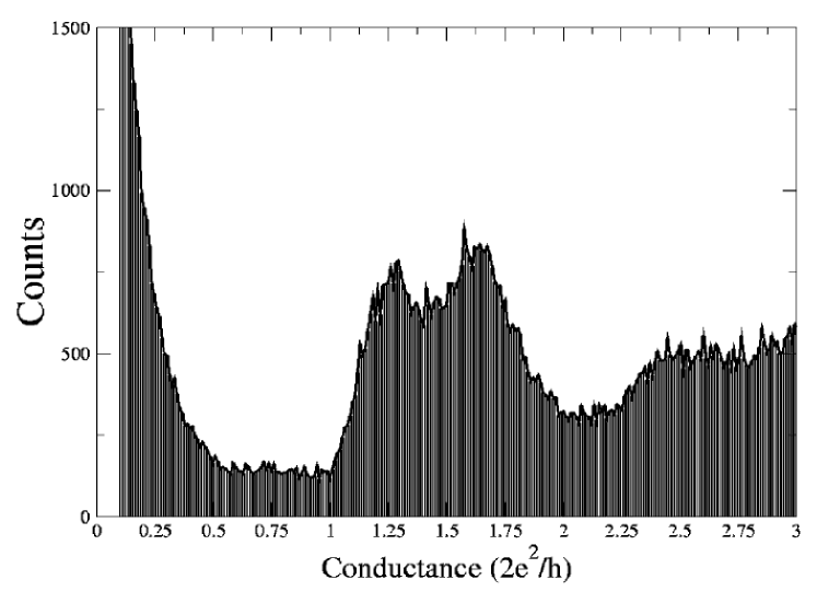
We recorded traces of conductance as a function of the relative tip-sample distance as the two electrodes were brought together and separated. In every trace, we made a deep tip-sample indentation in order to prevent the repetition of the same atomistic configurations and to assure the clearness of the contacts. Afterward, the traces were collected to build a conductance histogram such as the one shown in Fig. 1.
Histograms, similar to the aforementioned, for the first stages of conduction in Ni nanocontacts have been studied before Agraït et al. (2003); Sirvent et al. (1996); Untiedt et al. (2004). There a broad peak around 1.6 , where is the quantum of conductance, has been reported as the first peak after vacuum tunneling. This peak is attributed to the cases in which the contact consists of a single atom. On the other hand, for values of conductance below the one-atom peak, we can notice a large amount of data coming from tunneling. This effect is stronger in Ni than in other metals, such as Au, since for Ni, some of the traces show a smooth transition from tunneling to contact without a jump Untiedt et al. (2007).
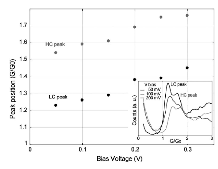
Here, we have studied in detail the lowest conductance peak after tunneling and noticed that, indeed, it is not a single broad peak, but the superposition of two at around 1.2 and 1.5 . The position of these peaks slightly changes for different contacts, and this may be the reason why they have not always been clearly resolved. We have performed separated conductance histograms from the traces for the cases of either forming or breaking the contacts. There we find a different ratio in the height of the peaks, being in the case of breaking traces the peak at 1.2 , in general, higher than the one at 1.5 and vice versa in the case of making the contacts. Finally, we notice a dependence of the position of the peaks with the bias voltage with a variation of even 0.3 in a voltage range of 300 mV, as shown in Fig. 2.
To the best of our knowledge, the described features have not been previously reported for any material. Normally, the peaks in the conductance histograms do not change as a function of the bias voltage Agraït et al. (2003), and are equal for the cases of breaking or forming the contacts. In order to understand our observations, one should first try to identify all the possible atomic configurations that could lead to a conductance in between 1 and 2 in Ni nanocontacts, and next look for the reasons that make the value of conductance to be so dependent on the bias voltage. In the following discussion, we will address the first question.
III Mechanical Properties
The dynamic deformation of Ni nanowires upon stretching until failure has been studied using molecular dynamics with empirical potentials. This type of modeling has provided significant information about the atomic scale processes occurring during deformation of nanowires Landman et al. (1990); Todorov and Sutton (1993). In this particular work, we focus on the last stages before failure of Ni nanocontacts. The interatomic potential for Ni developed by Mishin et al. Mishin et al. (1999) was used in these calculations. This potential has been fitted to reproduce the stacking fault energy of Ni. In all calculations, deformation is achieved by displacing the outer two layers of atoms on each side of the simulation box a fixed distance every 1000 simulation steps, similar to what is done by other authors Sørensen et al. (1998). Two different deformation velocities were used, 1 and 10 m/s Sørensen et al. (1998).
The dependence of different parameters on the deformation and, in particular, on the last stages before failure has been studied. On one hand, we have compared the deformation of different system sizes, between 77 and 2645 atoms, with initial cross sections between 1.5 and 3.5 , where is the lattice parameter, =3.52 Å , for the case where tension is applied along the [1 0 0] direction. The dependence with crystallographic direction has also been studied for systems with similar number of atoms (between 610 and 658) and for directions [1 0 0], [1 1 1], [1 1 0], and [1 1 2]. All these calculations were performed at a fixed temperature of 4.2K by rescaling the velocities of all atoms. Finally, the dependence with temperature was also studied for the particular case of deformation along the [1 0 0] direction and a cross section of 2.
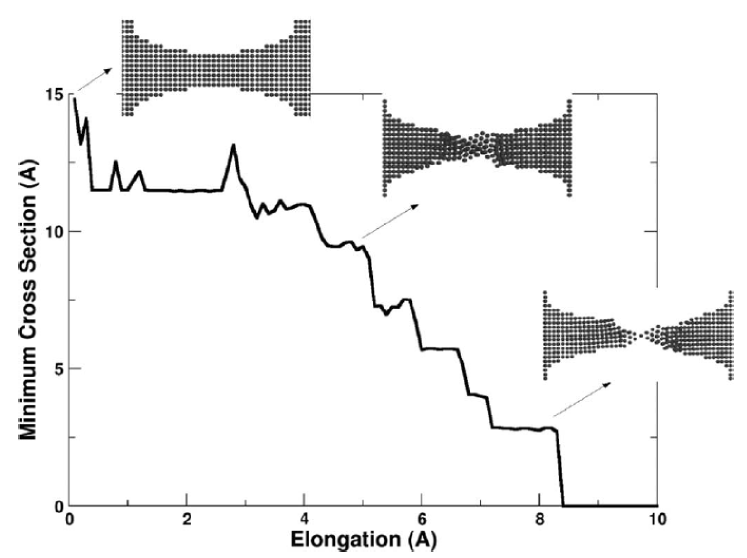
The minimum cross section perpendicular to the applied tension is computed every 1000 steps following the method developed by Bratkovsky et al. Bratkovsky et al. (1995). This method allows us to compare the results of deformation along different crystallographic directions. Fig. 3 shows the minimum cross section as a function of elongation obtained for one particular case with 2645 atoms and deformation along the [1 0 0] direction. The insets show several configurations during the deformation: the initial configuration, an intermediate configuration that is particularly stable, and the final configuration, which, in this case, consists of a single atom, a monomer, connecting the two sides of the nanowire. The mechanisms for deformation at this scale have been studied in detail by other authors Sørensen et al. (1998). Consistent with their work, we observe the sliding of planes during deformation (such as in the intermediate inset in Fig. 3) that results in a narrowing of the wire. This results in preferential configurations, reflected in the plateaus observed in Fig. 3.
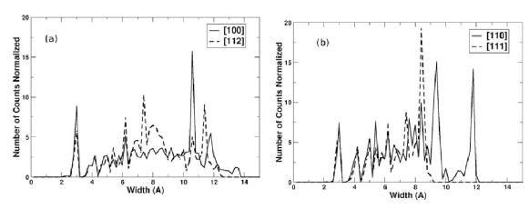
The dependence of the deformation on the stretching direction has been studied for [1 0 0], [1 1 1], [1 1 0], and [1 1 2] directions. Static calculations to obtain the energy to fracture along these different directions show that the [1 1 2] direction has the lowest energy per unit surface, followed by the [1 0 0], [1 1 0], and [1 1 1] directions. However, this behavior could be different during dynamic deformation. For each direction, calculations were repeated 100 times in order to gain some statistics and obtain a histogram of cross sections. Fig. 4 shows the histograms obtained for all crystallographic directions with clear peaks at particular cross sections. These preferential cross sections do not depend on the system size. Histograms obtained from smaller systems result in peaks located at exactly the same positions. It is interesting to point out that the first four peaks appear in all cases. These correspond to the smallest cross sections, consisting of less than three atoms across.
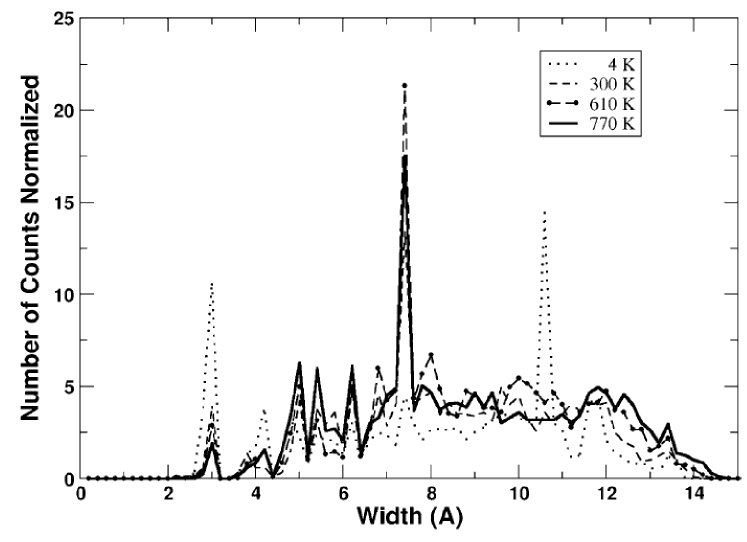
These first peaks are also very stable with temperature. Fig. 5 shows the histograms obtained for four different temperatures, 4.2K as before and 300K, 610K, and 770K. These histograms were obtained from 25 independent calculations and for the [1 0 0] direction. Notice that from 4.2K to room temperature, there is a strong reduction in the first peak. Therefore, the contact breaks very rapidly at high temperatures. On the contrary, structures with cross sections of two or three atoms seem to be very stable with temperature. For wider structures, there is not a clear peak at high temperature as in the case of 4.2K, which seems to point to very different types of structures possible when temperature increases. The dependence with temperature of these structures has been studied previously by other authors Hasmy et al. (2001).
In what follows, we focus on the final stage before failure of these nanocontacts. Two structures have been identified: a monomer, where a single atom acts as a bridge between the two contacts, and a dimer,where two atoms aligned forming a bridge between the two sides of the wire. These two configurations are shown in the insets of Fig. 6, (a) being the monomer and (b) the dimer. In order to identify the dimer, we have calculated the total number of neighbors for each atom and the number of neighbors to the left of the atom position and to the right along the z-direction. In this manner, it is easy to identify a dimer since it will consist of two neighboring atoms each one with only one neighbor on one side, one atom to the left, the second one to the right. From all the cases computed including all crystallographic directions (4 0 0), a total of 82% form a dimer before failure, while only 18% break from the monomer. In the cases studied in detail, the monomer is formed before the dimer, but, in a few cases, the contact breaks before forming the dimer.
IV Transport properties
We have finally computed the transport properties of the two possible types of configurations, i.e., a monomer and a dimer, before failure. The basics to calculate the zero-bias, zero-temperature conductance, , in a metallic nanocontact are contained in Landauer′s formalism, where is proportional to the quantum mechanical transmission probability of the electrons at the Fermi energy,
| (1) |
In this expression, the contributions from spin up (majority) and spin down (minority) channels have been explicitly separated, while the contribution from all the orbital channels has been condensed in . For simplicity, we assume no spin mixing due to either spin-orbit scattering or noncollinear magnetic structures at the bridge. The detailed electronic and magnetic structure of the nanocontact is important, and, in order to achieve a quantitative level of agreement with experiments, one has to rely on first-principles or ab initio calculations. These calculations are performed with our code ALACANT Palacios et al. (2001, 2002); Louis et al. (2003); qui . The details of the calculation have been presented in previous publications Palacios et al. (2001, 2002); Louis et al. (2003); qui . Essentially, one computes the self-consistent Kohn-Sham Hamiltonian for the narrowest part of the nanocontact, replacing the rest of atoms by a self-energy calculated based on a parametrized Bethe lattice.
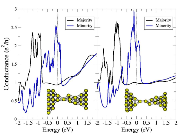
Using as input data two representative atomic configurations, as those shown in Fig. 6, the transmission spectrum of these two structures has been calculated at the local spin density approximation (LSDA) level, and close attention has been paid to the choice of basis set for the central part of the nanocontact. As expected for Ni, majority conduction is smooth as a function of energy due to the -like nature of this channel, while minority conduction is strongly fluctuating close to the Fermi energy due to the -like character of this channel Jacob et al. (2005). Interestingly, the average value of the conductance around the Fermi level for both the examples lies somewhere in the vicinity of 1.6(), which agrees fairly well with the value of the highest conductance peak in the histogram (see Fig. 1). Remarkably, this value can only be obtained with an LSDA Kohn-Sham potential. The use of generalized gradient corrected functionals or hybrid functionals reduces strongly the conductance for minority electrons, leaving no possible explanation for the high-conductance peak.
As far as the origin of the low-conductance peak, one could possibly attribute it to the presence of a domain wall at the narrowest section. Domain walls have a small but sizeable effect on the conductance of Ni nanocontacs, reducing it by an amount that agrees in magnitude with the conductance of the lowest peak. More experimental and theoretical work is, however, needed in this direction before this hypothesis can be confirmed.
Acknowledgements.
This work was supported in part by the Ministry of Education and Science (MEC) of Spain under Grant MAT2007-65487, Grant FIS2004-02356, and Grant CONSOLIDER CSD2007-00010 and in part by the Generalitat Valenciana under Grant ACOMP06/138. The works of M. J. Caturla and C. Untiedt were supported by the Spanish McyT. F. under a “Ramón y Cajal” grant.References
- Muller et al. (1992) C. J. Muller, J. M. van Ruitenbeek, and L. J. de Jongh, Phys. Rev. Lett. 69, 140 (1992).
- Agraït et al. (1993) N. Agraït, J. G. Rodrigo, and S. Vieira, Phys. Rev. B 47, 12345 (1993).
- Agraït et al. (2003) N. Agraït, A. Levy-Yeyati, and J. M. van Ruitenbeek, Physics Reports 377, 81 (2003).
- Viret et al. (2002) M. Viret, S. Berger, M. Gabureac, F. Ott, D. Olligs, I. Petej, J. F. Gregg, C. Fermon, G. Francinet, and G. L. Goff, Phys. Rev. B 66, 220401 (2002).
- Untiedt et al. (2004) C. Untiedt, D. M. T. Dekker, D. Djukic, and J. M. van Ruitenbeek, Phys. Rev. B 69, 081401 (2004).
- Sirvent et al. (1996) C. Sirvent, J. G. Rodrigo, S. Vieira, L. Jurczyszyn, N. Mingo, and F. Flores, Phys. Rev. B 53, 16086 (1996).
- Untiedt et al. (2007) C. Untiedt, M. J. Caturla, M. R. Calvo, J. J. Palacios, R. C. Segers, and J. M. van Ruitenbeek, Physical Review Letters 98, 206801 (pages 4) (2007).
- Landman et al. (1990) U. Landman, W. D. Luedtke, N. A. Burnham, and R. J. Colton, Science 248, 454 (1990).
- Todorov and Sutton (1993) T. N. Todorov and A. P. Sutton, Phys. Rev. Lett. 70, 2138 (1993).
- Mishin et al. (1999) Y. Mishin, D. Farkas, M. J. Mehl, and D. A. Papaconstantopoulos, Phys. Rev. B 59, 3393 (1999).
- Sørensen et al. (1998) M. R. Sørensen, M. Brandbyge, and K. W. Jacobsen, Phys. Rev. B 57, 3283 (1998).
- Bratkovsky et al. (1995) A. M. Bratkovsky, A. P. Sutton, and T. N. Todorov, Phys. Rev. B 52, 5036 (1995).
- Hasmy et al. (2001) A. Hasmy, E. Medina, and P. A. Serena, Phys. Rev. Lett. 86, 5574 (2001).
- Palacios et al. (2001) J. J. Palacios, A. J. Pérez-Jiménez, E. Louis, and J. A. Vergés, Phys. Rev. B 64, 115411 (2001).
- Palacios et al. (2002) J. J. Palacios, A. J. Pérez-Jiménez, E. Louis, E. SanFabián, and J. A. Vergés, Phys. Rev. B 66, 035322 (2002).
- Louis et al. (2003) E. Louis, J. A. Vergés, J. J. Palacios, A. J. Pérez-Jiménez, and E. SanFabián, Phys. Rev. B 67, 155321 (2003).
- (17) URL http://www.guirisystems.com/alacant.html.
- Jacob et al. (2005) D. Jacob, J. Fernández-Rossier, and J. J. Palacios, Physical Review B (Condensed Matter and Materials Physics) 71, 220403 (pages 4) (2005).