Spin polarization control by electric stirring: proposal for a spintronic device
Abstract
We propose a spintronic device to generate spin polarization in a mesoscopic region by purely electric means. We show that the spin Hall effect in combination with the stirring effect are sufficient to induce measurable spin polarization in a closed geometry. Our device structure does not require the application of magnetic fields, external radiation or ferromagnetic leads, and can be implemented in standard semiconducting materials.
pacs:
03.65.Vf, 05.10.Gg, 05.40.CaEfficient control over electronic spins has a potential to transform the design principles in semiconductor electronics. Spins provide additional degrees of freedom, which can be used as mobile bits of information and manipulated on much faster time-scales than charges. Spintronic devices, such as the giant-magnetoresistive effect based devices, have already found industrial applications dyakonov-book . However, realizing the full potential of spintronics requires integrating spin-based devices with traditional semiconductor technology.
Various techniques have been proposed to manipulate spins in semiconductors. The most accessible ones include the application of an external magnetic field or polarized radiation dyakonov-book , but they do not have the potential for implementing a single-chip device. Another possibility is to generate spin-polarized currents by coupling semiconducting and ferromagnetic materials. This approach, while promising, currently faces many technological complications dyakonov-book . Thus, it is most desirable to create spintronic components which involve neither external optical/magnetic fields nor coupling to ferromagnetic materials for their operation. It is preferred that such components be implemented in standard non-magnetic semiconductors, such as Si or GaAs. For this reason, the idea of using microwave fields in spintronic applications has attracted much attention dyakonov-book ; aronov ; loss-nature ; martin . However, these effects still rely on the presence of external magnetic fields to break the time-reversal symmetry or appear as bulk effects for which applications to building new spintronic components remain obscure.
In this Letter, we propose a device structure to generate spin polarization in a mesoscopic region. In our setup, the time-reversal symmetry is broken by purely electric means when multiple AC gate voltages, working with the phase shifts different from or , are applied. Periodic variation of parameters in a closed conducting system leads to the stirring effect (SE) stirring-quantum ; sinitsyn-09review , which is a sort of pump effect niu-pump ; vavilov-review with a distinctive feature that currents during SE are induced in a closed geometry, without sinks or sources of electrons. These currents have to be circulating.
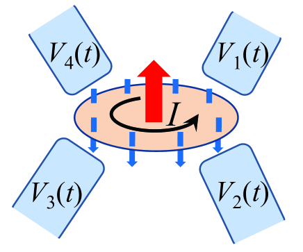
Consider, for example, a mesoscopic conducting sample, which we will call a conducting island. In Fig. 1, four gates with a voltage signal changing with time according to the law
will induce the SE so that the electric current will flow in a preferred (clockwise or counterclockwise) direction inside the island. Let the conducting island be made of a material exhibiting the spin Hall effect murakami-she ; sinova-she ; kato ; wunderlich (SHE). Then, when circulating charge currents are excited, electrons with a certain spin polarization will deflect towards the island’s center as it is shown in Fig. 1 creating the desired spin polarization.
We take the size of conducting island to be sufficiently large to disregard the discreteness of electron energy spectrum. Depending on the screening strength, the gate voltages can create circulating currents in the whole island or only in a localized region near the boundary. The former regime is more desirable and is realizable in low or moderately doped semiconductor islands whose dimensions do not exceed several m (see calculations below). The second regime is more relevant to heavily doped semiconductor or metal islands. By solving drift diffusion equations near the interface between regions with zero and nonzero charge currents, one can find that spin polarization decays at a distance comparable to the spin diffusion length from the interface, where is the charge diffusion coefficient and is the spin relaxation time. To find substantial spin polarization near the center of the island, in the second regime, the size of the region, unperturbed by gate voltages, should not be much larger than . Typically, microns for GaAs. Hence, due to the finite spin life time, the size of the conducting island can be several microns. In our numerical simulations (see below), we consider a situation when the diameter of the island is smaller than . In this case, substantial spin polarization at the island center is obtained.
We note that there exists another mechanism for spin polarization in our setup. Microscopically, spin-orbit coupling is described by the expression where is the operator of angular momentum and is the spin operator and is a spin-orbit coupling constant. Circulating currents carry a nonzero angular momentum, and hence lead to energy imbalance for spins with opposite orientations. This mechanism can be functional even in devices with nanoscale dimensions. However, it is expected that the SHE is the dominant mechanism for non-zero spin polarization, and, therefore, only the SHE is included in our calculations.
In the drift-diffusion approximation, the z-component of spin current is given by
| (1) |
where is the spin density imbalance, is the density of spin-up (-down) electrons, is a unit vector in the direction which is transverse to the stirring plane and is the charge current density. The first term in the RHS is due to spin diffusion, and the second term describes the SHE. Experimentalkato and theoreticalengel studies in GaAs as well as Al samples determined the relative strength of the spin Hall current to the charge current as . We use a linear dependence of spin current on the charge current, which describes the extrinsic mechanism of the SHE. It is believed to dominate in n-doped GaAs kato .
Consider a case of a uniformly circulating electron current , where is the density of conducting electrons, is the rotation frequency, and is the unit vector in the azimuthal direction. In the polar coordinates, the drift-diffusion equation with spin currents (1) and a phenomenological spin relaxation term is given by
| (2) |
where and are coordinates of a point in the polar coordinate system. Eq. (2) has a simple stationary solution that describes a rotating electron gas in a conductor of infinite diameter and
| (3) |
It cannot be valid near the boundary of a finite system, however, it provides a good estimate of the spin polarization far away from the boundary inside a sufficiently large structure. Taking , , and we find that , i.e. about 0.1% of electrons will be spin polarized near the center of the structure.
The application of an AC gate voltage is akin to the application of a rotating electric field. At optical frequencies, such a field is known to induce transitions between the valence and conduction bands of semiconductors, creating spin polarization. In our device, this field rotates with a microwave frequency and cannot induce spin polarization via the conventional mechanism. It can, however, excite circulating currents pershin-piermarocchi .
We solve numerically a system of two-component drift-diffusion equations supplemented by the Poisson equation. Our numerical scheme is similar to those used in Ref. pershin-diventra, with the only difference that now we are solving equations in 2D. The Poisson equation is solved in a larger area enclosing the conducting island with the boundary condition that the potential at the boundary of the larger area is presented by the rotating electric field. The rotating electric field can be written as , where and are the electric field amplitude and angular frequency, and are unit vectors in the and directions, and corresponds to a circular polarization.
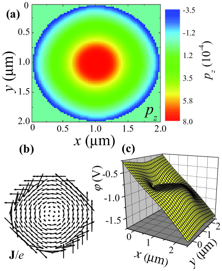
Fig. 2 shows a representative result of our calculations. Here, we consider a moderately doped GaAs island of a circular shape. At the selected value of electron density (cm-3), the electric field penetrates deep inside the island creating circulating currents which are not limited to the surface (Fig. 2(b)). The spin polarization calculated as , where denotes averaging over the rotating field period, has a magnitude () at the center.
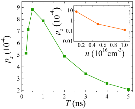
In Fig. 3, we plot the spin polarization magnitude at the island center as a function of the rotating field period and electron density (inset). When we start to decrease from 5ns, increases first as is expected from Eq. (3), and has a maximum at ns and then decreases. This decrease is possibly related to the resonance nature of circulating current excitation or strong spin densities mixing in highly non-equilibrium environment. An increase of the electron density results in a decrease of the spin polarization (see the inset in Fig. 3) mainly because at higher electron densities, the circulating currents are limited to the surface regions. We note that in a real setup, this effect should be less important because the finite viscosity of the electron fluid as well as the finite thickness of the island are not captured by our 2D calculations. Then, when a finite thickness of the island is taken into account, the exponential 3D screening reduces to a power-law type stern and the electric field penetrates deeper into the island creating stronger SE.
In conclusion, we proposed a spintronic device that generates a spin polarization in a localized region of a semiconductor by purely electric means. Importantly, our device structure does not require the application of magnetic fields, external radiation or ferromagnetic leads, and can be implemented in standard semiconductor materials. The novelty of our approach is in considering the combination of two effects, namely the spin Hall effect and the stirring effect. Our numerical simulations confirm that the induced spin polarization is sufficiently strong to be observable by the Kerr rotation technique. Our spintronic device can be used to generate spin polarized currents or to control the magnetization of a nanomagnet placed at the center of the conducting island, e.g. by doping Mn ions.
Acknowledgments. This work was funded in part by NSF grant DMR 0804199, and the US DOE under Contract No. DE-AC52-06NA25396.
References
- (1) M. I. Dyakonov, “Spin Physics in Semiconductors”, Springer series in solid-state science 157, Berlin (2008).
- (2) A. G. Aronov and Yu. B. Lyanda-Geller, Pis’ma Zh. Eksp. Teor. Fiz. 52, 663 (1990).
- (3) M. Duckheim and D. Loss, Nature Physics 2, 195 (2006).
- (4) A. Shnirman and I. Martin, EPL 78, 27001 (2007).
- (5) M. Hiller, T. Kottos, and D. Cohen, EPL 82, 40006 (2008).
- (6) N. A. Sinitsyn, J. Phys. A: Theor. Comp. 42, 193001 (2009).
- (7) Q. Niu and D. J. Thouless, J. Phys. A 17, 2453 (1984).
- (8) M. G. Vavilov, J. Phys. A: Math. Gen. 38, 10587 (2005).
- (9) S. Murakami, N. Nagaosa and S.-C. Zhang, Science 301, 1348 (2003).
- (10) J. Sinova, D. Culcer, Q. Niu, N. A. Sinitsyn, T. Jungwirth, and A. H. MacDonald, Phys. Rev. Lett. 92, 126603 (2004).
- (11) Y. Kato, R. C. Myers, A. C. Gossard, and D. D. Awschalom, Science 306, 1910 (2004).
- (12) J. Wunderlich, B. Kaestner, J. Sinova and T. Jungwirth, Phys. Rev. Lett. 94, 047204 (2005).
- (13) H.-A. Engel, B. I. Halperin, and E. I. Rashba, Phys. Rev. Lett. 95, 166605 (2005); H.-A. Engel, B. I. Halperin, and E. I. Rashba, Phys. Rev. Lett. 98, 036602 (2007).
- (14) Yu. V. Pershin and C. Piermarocchi, Phys. Rev. B 72, 245331 (2005); Yu. V. Pershin and C. Piermarocchi, Phys. Rev. B 72, 125348 (2005).
- (15) Yu. V. Pershin and M. Di Ventra, J. Phys.: Condens. Matter 20, 025204 (2008); Yu. V. Pershin and M. Di Ventra, Phys. Rev. B 79, 153307 (2009).
- (16) T. Ando, A. B. Fowler, and F. Stern, Rev. Mod. Phys. 54, 437 (1982).


