Pumping properties of the hybrid single-electron transistor in dissipative environment
Abstract
Pumping characteristics were studied of the hybrid normal-metal/superconductor single-electron transistor embedded in a high-ohmic environment. Two -long microstrip resistors of CrO with a sum resistance were placed adjacent to this hybrid device. Substantial improvement of pumping and reduction of the subgap leakage were observed in the low-MHz range. At higher frequencies , a slowdown of tunneling due to the enhanced damping and electron heating negatively affected the pumping, as compared to the reference bare devices.
One of the paramount applications of metallic single electron tunneling (SET) devices has been generation and detection of very low quantized currents, , for the purposes of charge metrology (see, e.g., Ref. Keller ). An important role plays the fundamental trade-off between the accuracy, usually requiring opaque tunnel barriers, and the pumping rates. Sophisticated algorithms are applied to operate the multi-junction and multi-gate SET pumps at a high accuracy level. High-frequency pumping (for example, at , ), or driving several pumps in parallel, in order to produce nA-currents, is theoretically possible AccuracyOfThePump , but technologically very challenging.
Recently, single-gate pumping has been demonstrated for the very simple SET structures, consisting of two ultrasmall Al/AlO/Cu Superconductor–Insulator–Normal metal (SIN) contacts, arranged either as NISIN Pekola-NaturePhysics or SINIS Kemppinen transistors. The pumping mechanism reproduces qualitatively the hold-and-pass strategy, known for a four-junction SET turnstile Geerligs . The mechanism is based on the charge hysteresis, arising due to the gap in the energy spectrum of the superconductor of the SIN junctions.
The pumping accuracy has been analyzed in detail in Refs. Pekola-NaturePhysics ; PekolaAverin . In particular, it was shown that for the SINIS type devices with a high charging energy, ( is the total capacitance of the transistor island), the lowest-order quantum leakage mechanism, a so-called Cooper-pair—electron (CPE) cotunneling, involves a coherent tunneling of three particles. This is an advantage of the hybrid devices, if compared, for example, to a 3-junction normal-state pump, subjected to two-electron cotunneling Pump . For realistic SINIS transistors with and a rectangular gate drive, the metrological accuracy of is predicted for the currents PekolaAverin ; Kemppinen2009 . The device simplicity opens a possibility of on-chip integration towards higher currents.

In this Letter, we address an important modification of the hybrid devices due to including dissipative environment, realized as high-ohmic on-chip microresistors. Our interest is motivated, on one side, by successful experiments on cotunneling suppression in the normal-state SET circuits R-pump . On the qualitative level, similar improvements of the fundamental accuracy are expected for the hybrid devices as well. On the other hand, the experimental hybrid pumping is often superimposed by a sub-gap leakage that is too strong to be explained by CPE cotunneling Pekola-NaturePhysics ; Kemppinen ; Kemppinen2009 , and possibly caused by structural non-idealities of the sample. This extra leakage has been described phenomenologically with a model suggested for the effect of Cooper-pair breaking Dynes . Here we show that, specifically to the hybrid devices, already the lowest-order model predicts accuracy improvement due to implementation of the resistors. The resistors are therefore expected to suppress a broad spectrum of unwanted processes of different perturbation orders. Whereas high-order tunneling usually produces a small current contribution only, a well-measurable leakage suppression can be an experimental evidence of the resistors efficiency.
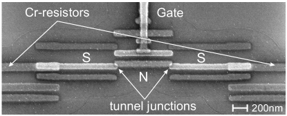
For our experiment, we fabricated hybrid devices of four different types: SINIS and NISIN type transistors, with and without chromium resistors (below we denote the devices with resistors as R-SINIS and R-NISIN). We used a trilayer PMMA/Ge/Copolymer mask and the shadow evaporation technique Shadow technique for the structure of CrO ( of Cr for the resistors, evaporated in O), Al (, oxidized after evaporation), and, finally, of Cr as a counter electrode. One of the R-SINIS devices is shown in Fig. 1. The basic results of this work are demonstrated, using transistor samples SINIS–1,2 and R-SINIS–1, and a reference single junction SIN–1 with the following parameters (respectively): total asymptotic resistances and and charging energies of the transistors and . The latter estimate is based on scaling the of the bare transistors with the tunneling resistance ratios. The resistance of Cr-lines was with a small non-linearity, observed as a zero-bias conductance dip at . The effective impedance seen by one of the identical junctions through the capacitance of the second one is . With our choice of impedance, , the reduction of the single-particle tunneling rates (and, thus, that of the pumping frequency) is still moderate IngNaz .

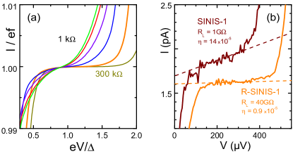
We modeled the single-electron tunneling rates in R-SINIS devices with the function formalism (see, e.g., Ref. IngNaz ), where can be interpreted as the probability of the exchange of energy between the SINIS transistor and its electromagnetic environment. The leakage was phenomenologically modelled by smearing the BCS density of states by introducing an appropriate lifetime of quasiparticles Dynes , resulting in a linear dc sub-gap currents, , for the unblocked bare devices. For low , which corresponds to the resistance of the Cr island itself, the simulated leakage is almost linear and close to that of the bare transistor. However for , the simulated sub-gap leakage is clearly nonlinear and it is suppressed by almost an order of magnitude at .
Figure 2(a) shows the pumping plateaus at , calculated for the broad range of impedances . We found that the high-ohmic environment extends the plateau and shifts its inflection point towards higher voltages. The minimum of the slope is found at the voltages and 1.15 for and , respectively. Interestingly, the minimum of the slope appears to be at the crossing point with , which might help locating the optimum operating point in practice. The lowest of possible slopes is expected for , being about 17 times lower than that in the case .
The experimental plateaus for the SINIS and R-SINIS devices are compared in Fig. 2(b), demonstrating the effect of the high-ohmic environment on the quantized current plateau at a low frequency. The figure of merit can be expressed by means of the leakage parameter , where is the lowest slope along the current plateau. Consistent with the model prediction, the resistor forced a considerable leakage suppression, corresponding to . Furthermore, the plateau of the R-SINIS sample extends to much higher voltages than has ever been observed for a bare hybrid turnstile Pekola-NaturePhysics ; Kemppinen ; Kemppinen2009 .

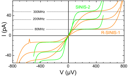
At higher frequencies, a noticeable slow-down of tunneling shows up for the R-SINIS devices, as compared to the bare ones. In the pumping – curves, Fig. 3, the rise to the plateau requires higher voltage, and the current versus gate-amplitude curve (not shown) demonstrates considerable back-tunneling effects Kemppinen2009 . At the frequencies above , the plateau starts to be deteriorated. According to our simulations, pumping in this frequency range is subject to intensive electron heating in the island. We note that, in the bare SINIS devices, the pumping plateaus were observed up to the high-frequency roll-off, , of our gate line.
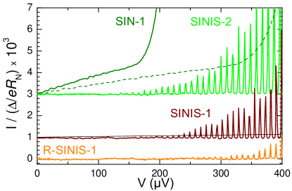
For a more detailed insight into the subgap processes, we studied dc envelopes, Fig. 4, of both SINIS and R-SINIS devices in a wide range of and . The high-ohmic environment is found to dramatically suppress the leakage, whereas the leakage magnitude appears to be of the same order with the slope of the pumping plateau. In our simulations, Fig. 2(a), we apply a phenomenological leakage slope (the thin solid line in Fig. 4), which was close to the averaged envelope and provided us with a correct prediction. However, the detailed mechanism is probably more complex and includes the processes beyond the lowest-order model. The dashed line in Fig. 4 shows the expectation for the bare transistor SINIS–2, in the gate-open state, plotted by appropriate scaling of the – curve of the representative junction SIN–1, designed to be a half of the SINIS layout. The scaling approach is physically relevant, if we assume that the subgap current appears due to unblocked but still correlated SET transport through the subgap ( e.g., ”poisoning”) states in the superconductor.

In contrast to the expected linear low-bias slope, the experimental envelopes show a clear voltage threshold, followed by a steep increase of the subgap current. One plausible interpretation for the peaks is Andreev reflection (AR), which here may be stronger than in other realizations Pekola-NaturePhysics ; Kemppinen ; Kemppinen2009 because of lower barrier quality of Al/AlO/Cr junctions. We note that at low charging energies, , AR cycles can be launched in the following way. First, a nonequilibrium quasiparticle (often generated in the superconducting leads by external noise or single photons due to imperfect filtering or shielding) tunnels from a lead to the island and gets trapped there due to the charge hysteresis induced by . Let us assume, e.g., that the gate charge is close to 0 and the island is trapped to the charge state 1. Now, AR cycles can contribute to the current by tunneling events between the charge states . The exact trapping mechanisms can vary greatly in different experiments, see, e.g., Ref. Hergenrother and the citations therein. Experimenting with several devices, we observed a large spread of leakage thresholds which may be related to the trapping-induced AR. The effective suppression of leakage peaks by the resistors indicates thus their efficiency against higher-order processes. Together with the requirement PekolaAverin , a radical improvement can be expected.
To conclude, we demonstrate the effect of high-ohmic environment on the hybrid turnstile. In the lower MHz-range, an order of magnitude improvement of the current plateaus was demonstrated in simulations and observed in experiment. Further analysis of the effect of the high-ohmic environment on the higher-order processes is necessary for developing the hybrid turnstile towards metrological applications. Also, the effect of cooling or heating of the island SET-cooling should be studied in more detail for further understanding of the device frequency limitations.
Fruitful discussions with M. Möttönen, O.-P. Saira, M. Meschke and V. Bubanja are gratefully acknowledged. A.K. thanks Väisälä foundation for financial support. The work was partially supported by Technology Industries of Finland Centennial Foundation, the Academy of Finland, and by the European Union through the project SCOPE.
References
- (1) M. W. Keller, A. L. Eichenberger, J. M. Martinis, and N. M. Zimmerman, Science 285, 1706 (1999); H. Scherer, S. V. Lotkhov, G.-D. Willenberg, and B. Camarota, IEEE Trans. Instrum. Meas. 58, 997 (2009).
- (2) H. D. Jensen and J. M. Martinis, Phys. Rev. B 46, 13407 (1992).
- (3) J. P. Pekola, J. J. Vartiainen, M. Möttönen, O.-P. Saira, M. Meschke, and D. V. Averin, Nature Physics 4, 120 (2008).
- (4) A. Kemppinen, M. Meschke, M. Möttönen, D. V. Averin, and J. P. Pekola, arXiv:0803.1563v2 (2008).
- (5) L. J. Geerligs, V. F. Anderegg, P. A. M. Holweg, J. E. Mooij, H. Pothier, D. Esteve, C. Urbina, and M. H. Devoret, Phys. Rev. Lett. 64, 2691 (1990).
- (6) D. V. Averin and J. P. Pekola, Phys. Rev. Lett. 101, 066801 (2008).
- (7) H. Pothier, P. Lafarge, C. Urbina, D. Esteve, and M. H. Devoret, Europhys. Lett. 17, 249 (1992).
- (8) A. Kemppinen, S. Kafanov, Yu. A. Pashkin, J. S. Tsai, D. V. Averin, and J. P. Pekola, Appl. Phys. Lett. 101, 172108 (2009).
- (9) A. B. Zorin, S. V. Lotkhov, H. Zangerle, and J. Niemeyer, J. Appl. Phys. 88, 2665 (2000). S. V. Lotkhov, S. A. Bogoslovsky, A. B. Zorin, and J. Niemeyer, Appl. Phys. Lett. 78, 946 (2001).
- (10) R. C. Dynes, J. P. Garno, G. B. Hertel, and T. P. Orlando, Phys. Rev. Lett. 53, 2437 (1984).
- (11) G. J. Dolan, Appl. Phys. Lett. 31, 337 (1977); J. Niemeyer, PTB-Mitt. 84, 251 (1974).
- (12) G. L. Ingold and Yu. V. Nazarov, in Single Charge Tunneling, edited by H. Grabert and M. H. Devoret (Plenum, New York, 1992), Chap. 2.
- (13) J. M. Hergenrother, J. G. Lu, M. T. Tuominen, D. C. Ralph, and M. Tinkham, Phys. Rev. B 51, 9407 (1995).
- (14) J. P. Pekola, F. Giazotto, O.-P. Saira, Phys. Rev. Lett. 98, 037201 (2007).