Coupled photonic crystal nanobeam cavities
Abstract
We describe the design, fabrication, and spectroscopy of coupled, high Quality () factor silicon nanobeam photonic crystal cavities. We show that the single nanobeam cavity modes are coupled into even and odd superposition modes, and we simulate the frequency and factor as a function of nanobeam spacing, demonstrating that a differential wavelength shift of 70 nm between the two modes is possible while maintaining factors greater than . For both on-substrate and free-standing nanobeams, we experimentally monitor the response of the even mode as the gap is varied, and measure factors as high as .
Photonic crystal cavities have been of great interest in recent years for their ability to strongly confine light in wavelength-scale volumes Noda05 ; Kuramochi06 ; Tanabe07 . The high Quality () factors and small mode volumes of these structures have enabled a wealth of new applications in areas as diverse as low-threshold lasers PainterScience ; loncar_apl_2004 , optical switching Tanabe05 , low power nonlinear optics McCutcheonPRB , cavity quantum electrodynamics Hennessy07 ; Englund07 , and chemical sensing Loncar ; DiFalco ; Kwon .
Single photonic crystal (PhC) cavities have now been optimized to a point where they can be treated as fundamental photonic components. To realize new functionality, it is essential to leverage the natural scalability of PhC cavities. For example, PhC cavities can be integrated into coupled resonator optical waveguides (CROWs) Yariv_crow to realize novel heterostructures capable of slowing light Notomi_Nphoton08 . There is also much recent excitement about the possibility of entangling the optical and mechanical degrees of freedom of a double cavity devicePovinelli ; Eichenfield_08 ; Chan_09 . To achieve optomechanical coupling, the cavities require a small mass and a flexible platform. These two properties are inherent to photonic crystal nanobeam cavities, which have been the subject of much recent investigation Sauvan ; Zain_08 ; McCutcheon_08 ; Deotare09 ; Notomi_1D ; Chan_09 . In addition to optomechanical effects, double cavity structures could facilitate adiabatic wavelength conversion. It has been predicted that the spacing of double planar PhC cavities can be varied to realize broad bandwidth dynamic resonance tuning while maintaining the high factor of the cavity mode Notomi_PRL . Here, we show the static tuning of double cavity modes by varying the cavity separation, thereby demonstrating a proof-of-principle of this effect.
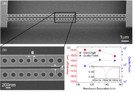
In this work, we study coupled photonic crystal nanobeam cavities consisting of two parallel suspended beams separated by a small gap, each patterned with a 1D line of holes, as shown in Fig. 1(a). The starting point for our double nanobeam design is our previously reported single PhC nanobeam cavity Deotare09 ; McCutcheon_08 . To briefly summarize the approach, we start with a 220 nm thick and 500 nm wide free-standing Si waveguide (nanobeam) which supports only a single transverse electric mode. The nanobeam is patterned with a linear array of air holes to introduce a stop-band in the guided mode bandstructure around 1550 nm. Near the middle of the beam, the hole size and spacing are tapered to introduce a defect potential capable of strongly localizing light. Optimization of the adiabatic 5-hole taper design leads to simulated -factors greater than , and we have experimentally measured in these single beam structures Deotare09 . We then created double cavity structures by positioning two such cavities side-by-side and varying the air gap between them. As expected from the physics of coupled harmonic oscillators, coupling generates new modes which are symmetric and anti-symmetric superpositions of the single cavity basis states, as shown in Fig. 2 Chan_09 . The energy splitting between the modes is dependent on the strength of the coupling, which in this case is determined by the size of the gap.

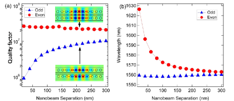
The mode profiles, factors, and resonant wavelengths are shown in Fig. 2 as a function of the gap, , between the nanobeams. The data were simulated with a 3D finite-difference time-domain code (Lumerical Solutions). For small , the coupling between the cavities is large, leading to a large splitting of the two modes. The wavelength of the odd mode changes little with , whereas the even mode disperses rapidly to longer wavelength as decreases. This behavior can be understood from the mode profiles in Fig. 2(a), which show that the even mode has an anti-node in the gap, whereas the odd mode has a node in the gap. The significant renormalization of the even mode renders it highly sensitive to . As shrinks below 100 nm, the field intensity of the gap anti-node grows and becomes the dominant feature in the mode, much like an air-slot cavity DiFalco ; Foubert ; Kwon ; Almeida . At the same time, the factor declines, since the photonic crystal tapering is not optimized for the significant redistribution of the mode energy into the slot between the nanobeams. These factors imply that the even mode would be a sensitive probe of the inter-beam distance, and thus useful for optomechanical applications Chan_09 ; Eichenfield_08 . It would also be useful in bio- and chemical-sensing, as the gap anti-node would be highly sensitive to perturbations in the external environment. As we will show below, it is only this mode which can be probed experimentally in our resonant scattering setup McCutcheon_05 ; Deotare09 .

In contrast to the significant alterations of the even mode, the odd mode is similar in profile to a superposition of two uncoupled single cavity modes. Because of the node in the gap, the cavities do not significantly perturb each other, and this results in a relatively small dispersion with . The factor, however, is substantially higher than that of the even mode, and in fact is approximately twice the factor of a single nanobeam cavity (). Intuitively, this is consistent with the larger mode volume, ()3, which is about twice that of the single cavity; the more extended real-space distribution of the fields results in a more localized -space distribution, and therefore a reduction in the radiative components within the light cone Srin_OE_03 .
The double nanobeam structures shown in Fig. 1 were fabricated on a silicon-on-insulator (SOI) wafer (SOITEC Inc) consisting of a silicon device layer of 220 nm, a SiO2 layer of 2m, and a thick silicon substrate. A negative e-beam resist, Foxx-17 (Dow Corning) diluted in six parts of methyl isobutyl ketone, was spun onto the sample at 5000 rpm to give a layer 135 nm thick, and patterns were defined using a 100 kV electron beam lithography system (Elionix). A negative resist simplifies the pattern-writing, since the only exposed region is along the nanobeam, and Foxx proved to be a robust etch mask for the RIE process. The resist was developed for 14 s in tetra-methyl ammonium hydroxide (% TMAH) followed by a thorough rinse in de-ionized water. The patterns were transfered to the silicon layer using reactive ion etching with a SF6, C4F8 and H2 plasma. The SiO2 sacrificial layer was removed using a hydrofluoric acid vapor etching tool (AMMT) deotare_hfvapor_2009 ; Deotare09 .
We experimentally probed our double nanobeam cavities using a cross-polarized resonant scattering technique McCutcheon_05 ; Englund07 . A tunable CW laser (Agilent) was focused onto the cavity from normal incidence with a microscope objective (numerical aperture = 0.5). The resonantly scattered reflected signal was analyzed in the cross polarization before being sent to an InGaAs detector. Recently, we used the same approach to measure factors as high as in single nanobeam cavities Deotare09 . Because the resonant excitation field drives the () fields in the coupled nanobeams in phase, this technique is primarily sensitive to the even mode. We note that in principle, the field gradient of the focussed spot could be exploited to excite the odd mode, as could butt-coupling or evanescent waveguide coupling techniques Srinivasan_04 ; Notomi04 ; Zain_08 . Fig. 1(c) shows the resonant wavelength and factor of the even mode for three different nanobeam separations. As predicted by our simulations (Fig. 2), the mode red-shifts as decreases. The factor varies between . Although this is more than an order of magnitude lower than predicted by simulations, this is a highly useful range for applications, and we expect increases as the fabrication quality of our structures improves.
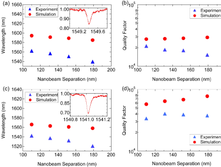
We also investigated the effect of the substrate on the cavity modes. As mentioned above, for small , the even mode field intensity is concentrated in the space between the cavities. This slot mode could be useful for bio- and chemical sensing, but to be robust in a liquid environment such a device would require the structural stability provided by a substrate. Due to the limited tuning range of our laser, these data were obtained from cavities with a size () of 136 nm, which is smaller than our optimal design of 146 nm (data shown in Fig. 1(c)). In Fig. 3(a) and (b), we present the results of our resonant scattering spectroscopy for unreleased, on-substrate nanobeam cavities (i.e. supported by SiO2). The Foxx resist was not removed for these cavities, since any etch process would also remove the substrate. However, we estimate that the resist layer remaining on top of the silicon nanobeams has a thickness less than 40 nm. The resonant wavelength and factor of the even mode are plotted as a function of . The resonance blue-shifts with increasing as the effective index of the cavity mode decreases. The experiment shows a larger dispersion than the simulation, likely reflecting the increasing role of e-beam lithography proximity effects for small gaps. The measured factors of are remarkably high for supported cavities Zain_08 , considering that the designs were optimized for free-standing nanobeams. Given the robust structure, high factors, and field intensity in the gap, the supported double nanobeam cavity is a promising approach to scalable, on-chip sensing applications.
Fig. 3(c) and (d) show the experimental data for the same cavities after the sacrifical SiO2 substrate was removed. The modes are blue-shifted compared to the results of Fig. 3(a), as expected from the decreased effective index of the air cladding compared to the oxide. The factors, however, are increased by a factor of due to the reduced leakage into the substrate.

In conclusion, by varying the spacing of two coupled nanobeam cavities, we have achieved resonance tuning over a 20 nm range for both on-substrate and free-standing structures while maintaining a relatively constant factor. This shows the same tuning principle that was predicted recently for double planar photonic crystal cavities Notomi_PRL , and the effect would be magnified for coupled nanobeams with smaller separations. The ability to tune the resonant wavelength of a cavity without adverse effects on the factor opens up new potential areas for research in optomechanics, adiabatic frequency conversion, and sensing.
Acknowledgements
This work is supported in part by Harvard’s National Science and Engineering Center, NSF grant ECCS-0701417, and NSF CAREER grant. Device fabrication was performed at the Center for Nanoscale Systems at Harvard. MWM would like to thank NSERC (Canada) for its support, and IWF thanks the NSF GRFP.
References
- [1] B. S. Song, S. Noda, T. Asano, and Y. Akahane. Ultra-high- photonic double-heterostructure nanocavity. Nature Materials, 4:207–210, 2005.
- [2] E. Kuramochi, M. Notomi, S. Mitsugi, A. Shinya, T. Tanabe, and T. Watanabe. Ultrahigh- photonic crystal nanocavities realized by the local width modulation of a line defect. Appl. Phys. Lett., 88:041112, 2006.
- [3] T. Tanabe, M. Notomi, E. Kuramochi, A. Shinya, and H. Taniyama. Trapping and delaying photons for one nanosecond in an ultrasmall high-q photonic-crystal nanocavity. Nature Photonics, 1:49–52, 2007.
- [4] O. Painter, R. K. Lee, A. Scherer, A. Yariv, J. D. O’Brien, P. D. Dapkus, and I. Kim. Two-dimensional photonic band-gap defect mode laser. Science, 284:1819–1821, 1999.
- [5] M. Loncar, T. Yoshie, A. Scherer, P. Gogna, and Y. M. Qiu. Low-threshold photonic crystal laser. Appl. Phys. Lett., 81:2680–2682, 2002.
- [6] T. Tanabe, M. Notomi, S. Mitsugi, A. Shinya, and E. Kuramochi. All-optical switches on a silicon chip realized using photonic crystal nanocavities. Appl. Phys. Lett., 87:151112, 2005.
- [7] M. W. McCutcheon, J. F. Young, G. W. Rieger, D. Dalacu, S. Frédérick, P. J. Poole, and R. L. Williams. Experimental demonstration of second-order processes in photonic crystal microcavities at submilliwatt excitation powers. Phys. Rev. B, 76:245104, 2007.
- [8] K. Hennessy, A. Badolato, M. Winger, D. Gerace, M. Atature, S. Gulde, S. Falt, E. L. Hu, and A. Imamoglu. Quantum nature of a strongly coupled single quantum dot-cavity system. Nature, 445:896–899, 2007.
- [9] D. Englund, A. Faraon, I. Fushman, N. Stoltz, P. Petroff, and J. Vučković. Controlling cavity reflectivity with a single quantum dot. Nature, 450:857–861, 2007.
- [10] M. Lončar, A . Scherer, and Y. Qiu. Photonic crystal laser sources for chemical detection. Appl. Phys. Lett., 82:4648–4650, 2003.
- [11] A. Di Falco, L. O’Faolain, and T. F. Krauss. Chemical sensing in slotted photonic crystal heterostructure cavities. Appl. Phys. Lett., 94:063503, 2009.
- [12] S.-H. Kwon, T. Sunner, M. Kamp, and A. Forchel. Optimization of photonic crystal cavity for chemical sensing. Opt. Express, 16:11709–11717, 2008.
- [13] A. Yariv, Y. Xu, R. K. Lee, and A. Scherer. Coupled-resonator optical waveguide: a proposal and analysis. Opt. Lett., 24:711713, 1999.
- [14] M. Notomi, E. Kuramochi, and T. Tanabe. Large-scale arrays of ultrahigh- coupled nanocavities. Nature Photonics, 2:741–747, 2008.
- [15] M. L. Povinelli, M. Loncar, M. Ibanescu, E. J. Smythe, S. G. Johnson, F. Capasso, and J. D. Joannopoulos. Evanescent-wave bonding between optical waveguides. Opt. Lett., 30:3042–3044, 2005.
- [16] M. Eichenfield, R. Camacho, J. Chan, K. J. Vahala, and O. Painter. A picogram and nanometer scale photonic crystal opto-mechanical cavity. arXiv:0812.2953v1 [physics.optics], 2008.
- [17] J. Chan, M. Eichenfield, R. Camacho, and O. Painter. Optical and mechanical design of a ”zipper” photonic crystal optomechanical cavity. Opt. Express, 17:3802–3817, 2009.
- [18] C. Sauvan, G. Lecamp, P. Lalanne, and J.P. Hugonin. Modal-reflectivity enhancement by geometry tuning in photonic crystal microcavities. Opt. Express, 13:245–255, 2005.
- [19] A. R. M. Zain, N. P. Johnson, M. Sorel, and R. M. De la Rue. Ultra high Quality factor one dimensional photonic crystal/photonic wire micro-cavities in silicon-on-insulator (SOI). Opt. Express, 16:12084–12089, 2008.
- [20] M. W. McCutcheon and M. Lončar. Design of a silicon nitride photonic crystal nanocavity with a Quality factor of one million for coupling to a diamond nanocrystal. Opt. Express, 16:19136–19145, 2008.
- [21] P. B. Deotare, M. W. McCutcheon, I. W. Frank, M. Khan, and M. Loncar. High quality factor photonic crystal nanobeam cavities. Appl. Phys. Lett., 94:121106, 2009.
- [22] M. Notomi, E. Kuramochi, and H. Taniyama. Ultrahigh- nanocavity with 1D photonic gap. Opt. Express, 16:11095–11102, 2008.
- [23] M. Notomi, H. Taniyama, S. Mitsugi, and E. Kuramochi. Optomechanical wavelength and energy conversion in high- double-layer cavities of photonic crystal slabs. Phys. Rev. Lett., 97, 2006.
- [24] K. Foubert, L. Lalouat, B. Cluzel, E. Picard, D. Peyrade, E. Delamadeleine, F. de Fornel, and E. Hadji. Near-field modal microscopy of subwavelength light confinement in multimode silicon slot waveguides. Appl. Phys. Lett., 93:251103, 2008.
- [25] V. R. Almeida, Q. Xu, C. A. Barrios, and M. Lipson. Guiding and confining light in void nanostructure. Opt. Lett., 29:1209–1211, 2004.
- [26] M. W. McCutcheon, G. W. Rieger, I. W. Cheung, J. F. Young, D. Dalacu, S. Frédérick, P. J. Poole, G. C. Aers, and R. L. Williams. Resonant scattering and second-harmonic spectroscopy of planar photonic crystal microcavities. Appl. Phys. Lett., 87:221110, 2005.
- [27] K. Srinivasan and O. Painter. Momentum space design of high- photonic crystal optical cavities. Opt. Express, 10:670–684, 2003.
- [28] P. B. Deotare, M. Khan, and M. Loncar. Vapor phase release of silicon nanostructures for optomechanics applications. Proc. SPIE, 7205:7205–09, 2009.
- [29] K. Srinivasan, P. E. Barclay, M. Borselli, and O. Painter. Optical-fiber-based measurement of an ultrasmall volume high- photonic crystal microcavity. Phys. Rev. B, 70:081306, 2004.
- [30] M. Notomi, A. Shinya, S. Mitsugi, E. Kuramochi, and H-Y. Ryu. Waveguides, resonators and their coupled elements in photonic crystal slabs. Opt. Express, 12:1551–1561, 2004.