Chemical functionalization on planar polysilane and graphane
Abstract
Two dimensional materials are important for electronics applications. A natural way for electronic structure engineering on two dimensional systems is on-plane chemical functionalization. Based on density functional theory, we study the electronic structures of fluorine substituted planar polysilane and graphane. We find that carbon and silicon present very different surface chemistry. The indirect energy gap of planar polysilane turns to be direct upon fluorine decoration, and the gap width is mainly determined by fluorine coverage regardless of its distribution on the surface. However, electronic structure of fluorine doped graphane is very sensitive to the doping configuration, due to the competition between antibonding states and nearly-free-electron (NFE) states. With specific fluorine distribution pattern, zero-dimensional and one-dimensional NFE states can be obtained. We have also studied the chemical modification with -OH or -NH2 group. Carbon seems to be too small to accommodate big functional groups on its graphane skeleton with a high concentration.
I introduction
Low-dimensional materials are expected to play a key role in nanotechnology. For example, it is desirable to use two dimensional materials to build electronics on flexible, lightweight, and cheap substrates like plastics. Guo08 Silicon is the fundamental semiconducting material in electronics. Due to its relatively large size, it prefers to form four covalent bonds in tetragonal coordination (sp3 hybridization) instead of forming strong planar bonds through sp2 hybridization. A stable two dimensional silicon material is planar polysilane, Takeda94 which is composed of a buckled hexagonal silicon framework and hydrogen atoms on both sides to saturate dangling bonds. Layered polysilane has been synthesized experimentally,Dahn93 ; si-exp and due to confinement effect, its electronic structure is different from bulk silicon. n1 ; n2 ; n3
After the successful experimental preparation of graphene,a1 carbon based materials become a rising star for two dimensional electronics. a2 ; a3 Compared to silicon, carbon have smaller radius, and stable bonds can be formed between carbon atoms within a plane. Therefore, the stablest two dimensional carbon structure is a hexagonal lattice, namely graphene. Carriers in graphene show massless Dirac Fermion behavior, and there is a symmetry between electron and hole in graphene. Since graphene is a semimetal, an energy gap must be opened before any ’graphenium’ microprocessor can be realized. A natural way for this purpose is to convert the sp2 bond in graphene to sp3 bond via hydrogenation. Such a carbon based sp3 structure is called graphane, the carbon analogue of planar polysilane, which was theoretically predicted to have a finite energy gap. b2 ; b3 Recently, graphane has been synthesized by hydrogen plasma treatment bh1 or by electron-induced dissociation of hydrogen silsesquioxane. Ryu08
For various electronics applications, it is very desirable to have the capability to fully control the energy gaps and electronic structures of planar polysilane and graphane. On-plane chemical functionalization is an important way towards this direction. Hydroxy group n2 ; n3 ; Deak92 substitution on planar polysilane has been studied. The product, siloxene, has a direct energy gap instead of the indirect one in unsubstituted planar polysilane. Deak92 ; n2 For two dimensional carbon based materials, previous electronic structure engineering attempts by chemical means mainly focuses on graphene nanoribbon edge modification. edge1 ; edge2 ; edge3 However, on-plane functionalization does not need to cut the graphene sheet, and it is expected to be a more feasible way to realize electronics on graphene (for example, by printing circuit on graphene). Although graphene oxide (GO) represents an on-plane chemically modified carbon material, it is mainly studied as an intermediate for massively production of graphene, g2 ; g4 ; g6 and the detailed structure of GO is still unclear. g1 ; g3 ; g5 ; g8 ; g9
Despite its importance, a systematical study of on-plane chemical functionalization for two dimensional silicon and carbon materials is still unavailable. Most importantly, how the electronic structure depends on the adsorption configuration of functional groups has not been discussed, which is very important for practical realization of electronic structure engineering in experiment. Another not considered important issue is the nearly-free-electron (NFE) states. NFE states are delocalized on the surface outside the atomic centers. f1 When they are close to the band edge, NFE states become a determining factor of the band gap width. f2 ; f3 ; f4 Since NFE states have unique space distribution, we expect their response to surface chemical functionalization to be different than other states.
In this article, we systematically studied the on-plane chemical modification on planar polysilane and graphane. Functionalization leads to significant electronic structure modification. Interestingly, electronic structure of fluorinated polysilane is much less sensitive to the F adsorption configuration than graphane. The remainder of the paper is organized as the following. In section II, we describe the computational details. The main results are discussed in section III. We first compare the electronic structure of two dimensional polysilane and graphane, and the NFE state on graphane is introduced. Then, we discuss different behaviors upon F substitution for these two systems. Other functional groups are finally discussed. Section IV concludes the paper.
II Computational Details
To investigate the geometric structures and electronic states of polysilane and graphane based systems, we performed first-principles DFT calculations with the Vienna Ab initio Simulation Package (VASP).n8 ; n9 Projector-augmented wave (PAW) method n10 ; n11 was used for electron-ion interaction, and the Perdew-Wang form n12 of the generalized gradient approximation (GGA) was adopted for electronic exchange and correlation. A kinetic-energy cutoff of 400 eV was selected for plane wave basis set. For pristine planar polysilane and graphane we chose a 11 unit cell, and a 22 supercell was used to consider chemical modification. The vacuum space between two neighboring two-dimensional sheets is larger than 15 Å, and dipole correction is applied to compensate artificial dipole interaction between neighoring supercells in the direction perpendicular to the plane. A 13131 -point mesh was used in geometry optimizations, and a 27271 grid was used for static electronic structure calculations. Geometry structures were relaxed until the force on each atom was less than 0.01 eV/Å and the the convergence criteria for energy is eV. A series of unit cells were scanned for each system to obtained the lattice parameters with the lowest energy. Charge populations were calculated using Bader’s atom in molecule (AIM) method based on charge density topological analysis.d2
III RESULTS AND DISCUSSION
III.1 Geometrical and electronic structures of planar polysilane and graphane
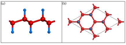
First, we compare the geometrical and electronic structures of planar polysilane and graphane. Both of them are composed of a buckled hexagonal plane of silicon or carbon, and hydrogen atoms on both sides of the plane to saturate the sp3 bonds (Fig. 1). The optimized Si-Si bond length is 2.36 Å, similar to its calculated bulk value (2.35 Å). Si-H bond length is 1.50 Å. The optimized C-C and C-H bond length in graphane is 1.54 and 1.11 Å, respectively. The C-C bond length in graphane is almost identical to its value in bulk diamond, and it is also in agreement with the previous theoretical results on graphane. b2 ; b3
Because its silicon or carbon atoms are sp3 hybridized, both planar polysilane and grphane have a significant energy gap (Figure 2). In agreement with Hirayama et al.,n3 we obtained a quasi-direct band gap about 2.20 eV for two dimensional polysilane, with the valance band maximum (VBM) at the point and the conduction band minimum(CBM) at the M point. The direct band gap at the point is just 0.12 eV broader. Graphane has an about 3.43 eV direct gap at , as also suggested by Sofo et al. b2
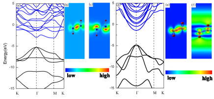
The VBM of polysilane is a Si-Si bonding state. Due to symmetry, it is two-fold degenerated at the point. The conduction band edge at point is the antibonding state between Si 3pz and H 1s orbitals, mainly distributed on Si. VBM of graphane have similar bonding character with planar polysilane. However, CBM state of graphane is notably different from that of ploysilane, where a strongly delocalized feature exists above and blow the graphane plane. Such a delocalized state is known as NFE state. f1 When it is pushed to the band edge, NFE state becomes a determining factor of the width of band gap. We note that the NFE-like character of its CBM state has not been noticed in previous study on graphane. b2
Why CBM of graphane is an NFE state, while that of polysilane is not? One reason is that the antibonding states of graphane are higher in energy than those of planar polysilane. On the other hand, NFE states of graphane are also strongly stabilized compared to those of planar polysilane. In fact, at the point, the lowest NFE states of polysilane and graphane locate at about 0.7 and 1.4 eV below the vaccum level, respectively. There are two possible reasons for the stabilization of the NFE states in graphane. First, compared to notably negatively charged hydrogen in polysilane, hydrogen atoms in graphane are almost neutral. A negatively charged surface is repulsive to electrons, and thus upshift NFE states. Second, the radius of carbon is smaller than silicon, which leads to a much smoother graphane surface than the polysilane surface. Actually, the distance between two hydrogen atoms in graphane is 1.35 Å shorter than that in polysilane. A smoother surface is expected to stabilize NFE states.
III.2 Fluorinated planar polysilane
Fluorine has a much larger electronegativity than hydrogen. Therefore, the substitution of hydrogen in planar polysilane by fluorine may lead to a significant electronic structure modification. We first consider the simplest case where all hydrogen atoms are replaced by fluorine atoms (100% F coverage). F substitution does not change the Si-Si bond length, and the optimized Si-F bond length is 1.63 Å.
The band structure of F-substituted polysilane (Fig. 3d) is very different from the unsubstituted system. The band gap (0.62 eV) becomes much smaller, and it is a direct gap at the point. Therefore, F-substituted polysilane will have a much higher luminous efficiency than bulk silicon. CBM of F-substituted polysilane at the point is mainly an antibonding state between Si and F molecular orbitals. Similar to siloxene, n3 the indirect gap to direct gap transition from unsubstituted to substituted polysilane may caused by stronger mixing with F 2s state at point, which pushes down the CBM at to lower than the local minimum at the M point. VBM is still mainly a Si-Si bonding state. However, compared to planar polysilane (Figure 2c), there is a small hybridization with the F 2s orbital.

It is also interesting to check the electronic structure evolution with the F coverage. Using a 22 supercell, we consider 25%, 50%, and, 75% F substitutions, which corresponds to 2, 4, and 6 fluorine atoms in the supercell, respectively. For 25% and 75% F coverages, we consider all possible F substitution configurations. For 50% F coverage, 6 configurations are considered. All calculated configurations for different F concentrations are plotted in Fig. 4.
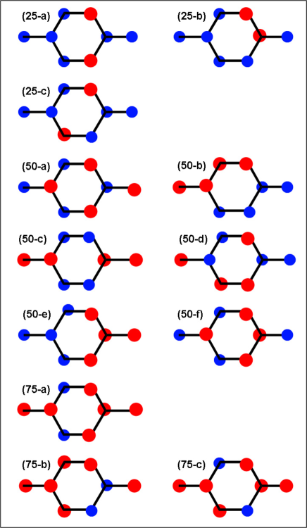
The energetically most stable configuration with different F coverage is 25-c, 50-c, and 75-c, respectively. However, the energy difference between different configurations for a certain F concentration is very small, typically within 0.1 eV. At the same time, with a certain F coverage, configuration difference has little effect on the band structure. As shown in Fig. 3, band gap decreases with the increase of the F coverage (Table 1).
In all configurations, CBM is mainly of antibonding character between Si-F or Si-H molecular orbitals. Since the Si-F antibonding state is lower in energy than the Si-H antibonding state (refer to the 100% F coverage case and the unsubstituted case), more weight of Si-F antibonding character leads to lower energy of the band. Therefore, as the percent of F substitutions increases, the energy of CBM significantly decreases.
VBM of fluorinated polysilane is a Si-Si bonding state with a small hybridization with F orbitals. The energy of VBM also slightly decrease with the F coverage, which can be understand by charge transfer between Si and F. Since fluorine has a larger electronegativity than silicon, an electron-transfer from Si to F is expected. Charge population Bader analysis shows that the amount of electrons transfer from Si to F increases with the increase of the F concentration (Table 1). As VBM is mainly a Si-Si bonding state, a positively charged Si skeleton will push down the VBM. Because the downshift of CBM is more significant than VBM, we still get smaller bang gap for strongly fluorinated polysilane.
| 0 | 25-a | 25-b | 25-c | 50-a | 50-b | 50-c | 50-d | 50-e | 50-f | 75-a | 75-b | 75-c | 100 | ||
| Si-F | 2.20 | 1.94 | 1.86 | 1.96 | 1.67 | 1.37 | 1.62 | 1.52 | 1.49 | 1.57 | 1.13 | 1.06 | 1.21 | 0.62 | |
| 3.46 | 3.37 | 3.38 | 3.38 | 3.32 | 3.32 | 3.32 | 3.32 | 3.32 | 3.32 | 3.26 | 3.27 | 3.26 | 3.19 | ||
| 0 | 0.30 | 0 | 0 | 0.60 | 0 | 0 | 0 | 0.30 | 0.30 | 0.30 | 0 | 0 | 0 | ||
| C-F | 3.43 | 3.43 | 4.94 | 4.86 | 2.60 | 4.56 | 5.44 | 5.16 | 4.54 | 4.46 | 4.17 | 4.14 | 4.77 | 3.10 | |
| 3.98 | 3.87 | 3.88 | 3.88 | 3.71 | 3.73 | 3.74 | 3.74 | 3.73 | 3.73 | 3.57 | 3.58 | 3.59 | 3.41 | ||
| 0 | 0.36 | 0 | 0 | 0.64 | 0 | 0 | 0 | 0.32 | 0.32 | 0.28 | 0 | 0 | 0 |
III.3 Fluorine functionalization on graphane
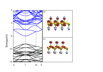
If all hydrogen atoms in graphane are substituted by fluorine, the C-C bond length will be slightly increased by 0.03 Å to 1.57 Å, and the optimized C-F bond length is 1.38 Å. As shown in Fig. 5, F substitution decrease the band gap of graphane to about 3.10 eV. CBM at the point is an antibonding state between C and F orbitals, and VBM is a mix of C-C bonding state and F 2s orbital. Compared to VBM of fluorinated two dimensional polysilane, the hybridization with the F orbitals here is stronger.
We also study different F coverage with all configurations listed in Fig. 4. For silicon, when the F coverage is fixed, different substitution configurations lead to similar band structures. Interestingly, the situation is totally different for F partially substituted graphane, where the F ordering plays a key role in the electronic structure of the doped systems.
With the 25% F coverage, we have three configurations. The 25-c configuration has similar band structure with 25-b. Therefore, in Fig. 6, we only plot the band structures for 25-a and 25-b. There is an about 1.5 eV difference between the energy gaps of 25-a and 25-b. VBM in both configurations is mainly a C-C bonding state with a small mixing of F 2p orbital. Just like F-substituted planar polysilane, its position slightly decreases with the F coverage. The CBM of 25-a is significantly lower than that of 25-b. CBM is mainly a NFE state similar to that of unsubstituted graphane (Fig. 2e). Since the NFE state is delocalized apart from the system, its energy can be easily affected by a shift of local vacuum level. A dipole layer on surface can modify the local vacuum level. In Table 1, we list the dipole moment for different configurations. Since, in 25-b and 25-c, the two fluorine atoms is distributed on two sides of the graphane plane, there is no net dipole moment for these two configurations. However, in 25-a, the two fluorine atoms is on the same side. Because fluorine atoms get electrons from the carbon skeleton, there is a dipole moment perpendicular to the surface, which lower the local vacuum level and thus also the NFE conduction band.
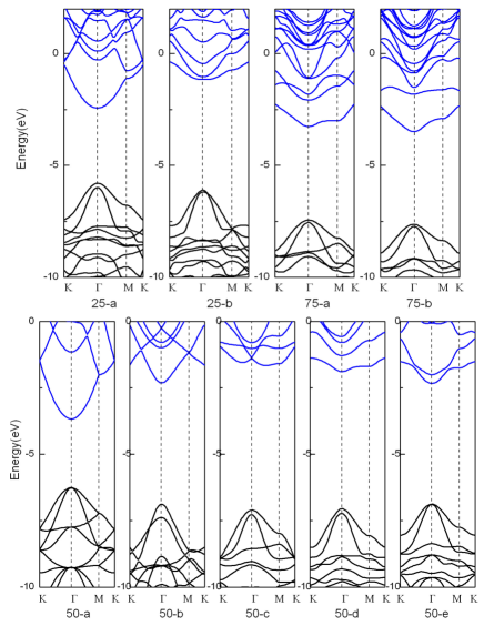
For 50% coverage, 50-f has similar electronic structure with 50-e, and will not be discussed here. In the 50-a configuration, all F atoms are on the same side, and the NFE-like CBM (distributed on the H side) is lowered by the dipole layer generated by charge transfer between C and F. As a result, the 50-a configuration has the smallest energy gap in all 50% F coverage configurations.
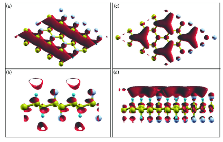
CBM of the 50-b configuration is an antibonding state between C and F molecular orbitals and the next two bands higher in energy at the point are mainly NFE states (Fig. 7a and 7b). Here, the lowest NFE state is higher than the lowest antibonding state. This is because that the F doping destroy the smooth H surface, which destabilize the NFE state. There is no dipole moment in 50-b, and the dipole stabilization mechanism does not help here. Interestingly, due to the chain configuration of H atoms, the NFE state forms one-dimensional distribution. One dimensional NFE state has potential application in electronics as an ideal transport channel when it is close to the Fermi level.
Surprisingly, an indirect band gap is obtained for 50-c. At the point, the lowest unoccupied band (LUB) is mainly a ribbon-like NFE state, but also with a strong hybridization with some C-H and C-F anti-bonding character. While the CBM at the -point between and M is mainly of antibonding character. This fact indicates a strong interaction between the NFE state and the antibonding state, which may be a reason for the indirect gap. In 50-d configuration, we also have hydrogen chains formed, which leads to two one-dimensional NFE bands (LUB+2 and LUB+3). However, in this configuration, hydrogen chains on the two sides of the graphane plane are not parallel.
Due to the dipole moment effect, CBM of 50-e is also a NFE state. Because neighboring H atoms form triangles, NFE states in 50-e are also of the shape of triangle (Fig. 7c and 7d). Such zero-dimensional NFE states demonstrate the flexibility to tune the distribution and energy of NFE states over two dimensional surface by chemical functionalization. Due to the smaller dipole moment compared to 50-a, the NFE state in 50-e is higher, which leads to a larger gap.
The band structures of 75-a and 75-b are shown in Fig. 6, and the band structure of 75-c is similar to 75-b. At the 75% F coverage, due to the low coverage of hydrogen, NFE state is not very stable, and CBM for all the three configurations is antibonding states between C and F molecular orbitals. Since the antibonding state is less affected by dipole moment, the gap difference between different configurations at 75% F coverage is much less than those at 25% or 50% F coverages.
III.4 Other functional groups
Hydroxy (-OH) and amine (-NH2) groups, both of which have multiple atoms, are also considered. For simplicity, we only discuss their 100% coverage on both sides and 50% coverage on one side (full coverage on that side, the 50-a configuration).
OH or NH2 functionalization does not change the lattice parameters of two dimensional polysilane, which is consistent with the relatively large Si-Si bond length and the week steric hindrance between functional groups. However, for smaller carbon, due to the repulsion between substituted radicals, the optimized C-C bond length upon OH or NH2 substitution is notably larger than that of graphane. With 50% and 100% OH coverage, the C-C bond length is 1.57 and 1.62 Å, respectively. For NH2 functionalization, the corresponding C-C bond length is 1.62 and 1.68 Å, respectively. The elongated C-C bond length indicates that it is difficult for graphane to accommodate large functional groups at a relatively high coverage, as also suggested by a previous GO structure study.b3
| coverage | 50% | 100% | coverage | 50% | 100% | |||
|---|---|---|---|---|---|---|---|---|
| Si-OH | Eg | 1.41 | 0.25 | C-OH | Eg | 1.85 | 2.21 | |
| 3.33 | 3.23 | 3.77 | 3.49 | |||||
| 0.08 | 0 | 0.25 | 0 | |||||
| Si-NH2 | Eg | 1.33 | 0.37 | C-NH2 | Eg | 1.79 | 1.97 | |
| 3.37 | 3.28 | 3.85 | 3.69 | |||||
| 0.30 | 0 | 0.10 | 0 |
As shown in Fig. 8, the energy gap is also decrease with the increase of the functional-group coverage for both OH and NH2 functionalized polysilane (Table 2). However, contrast with the F substitution case, VBM rise with the increase of the functional-group coverage. This may due to stronger mixing between Si-Si bonding states and N or O 2 orbitals, since they are higher than F 2 orbital and more close to the Si orbital. The strong hybridization between Si and O or N orbitals is consistent with the split VBM, which is degenerated in fluorinated polysilane. CBM at the point is mainly of the antibonding character between Si-O or Si-N molecular orbitals.

For both OH and NH2 doped graphane, we obtain a smaller gap for the 50% coverage compared to the 100% case. This is because the NFE state on the hydrogen atom in the 50% coverage case is lowered by the dipole layer developed in the system. In all four cases, VBM is a C-C bonding state mixed with O or N 2p orbitals. The mixing is very strong, which leads to an even larger splitting of VBM at the point compared to OH or NH2 substituted planar polysilane. The position of VBM is almost not affected by the functional group coverage, which indicate that the N and O 2p orbitals are close in energy to the C-C bonding state.

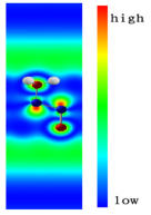
CBM of 100% OH covered graphane is also the antibonding states of C and O molecular orbitals. But for 100% NH2 covered graphane, CBM has a significant NFE-like character due to the hydrogen atoms in the radicals (Fig. 10). Such kind of NFE states provide more flexibility to use NFE state to tune the electronic and optical properties of two-dimensional materials.
IV conclusions
In summary, we have calculated the on-plane chemical modification of two dimensional polysilane and graphane. Chemical functionalization can change the indirect gap in planar polysilane to a direct gap, which will strongly modify the optical properties of the system. For fluorinated polysilane, the gap decreases with the F coverage, independent on the F adsorption configurations. However, the electronic structure of fluorinated graphane is sensitively dependent on the F doping geometry. This is because the NFE states of graphane is close to the conduction band edge. Energy of NFE states is more sensitive to the local vacuum potential and the doping structure. Functionalization by OH and NH2 groups is also discussed.
Acknowledgements.
This work is partially supported by NSFC (20803071, 50721091, 20533030, 50731160010), by MOE (NCET-08-0521), by FANEDD (2007B23), by the National Key Basic Research Program (2006CB922004), by the USTC-HP HPC project, by the SCCAS and Shanghai Supercomputer Center.References
- (1) Guo, X.; Silva, S. R. P. Science 2008, 320, 618.
- (2) Takeda, K.; Shiraishi, K. Phys. Rev. B 1994, 50, 14916.
- (3) Dahn, J. R.; Way, B. M.; Fuller, E.; Tse, J. S. Phys. Rev. B 1993, 48, 17872.
- (4) Nakano, H.; Ohtani, O.; Mitsuoka, T.; Akimoto, Y.; Nakamura, H. J. Am. Ceram. Soc. 2005, 88, 3522.
- (5) Takeda, K.; Shiraishi, K. Phys. Rev. B 1989, 39, 11028.
- (6) Van de Walle, C. G.; Northrup, J. E. Phys. Rev. Lett. 1993,70, 1116.
- (7) Hirayama, M.; Nakamura, J.; Natori, A. e-J. Surf. Sci. Nanotech. 2006, 4, 528.
- (8) Novoselov, K. S.; Geim, A. K.; Morozov, S. V.; Jiang, D.; Zhang, Y.; Dubonos, S. V.; Grigorieva, I. V.; Firsov, A. A. Science 2004, 306, 666.
- (9) Geim, A. K.; Novoselov, K. S.; Nature Mater. 2007, 6, 183.
- (10) Katsnelson, M. I. Mater. Today 2007, 10, 20.
- (11) Sofo,J. O.; Chaudhari, A. S.; Barber, G. D. Phys. Rev. B 2007, 75, 153401.
- (12) Boukhvalov, D. W.; Katsnelson, M. I.; Lichtenstein, A. I. Phys. Rev. B 2008, 77, 035427.
- (13) Elias, D. C.; Nair, R. R.; Mohiuddin, T. M. G.; Morozov, S. V.; Blake, P.; Halsall, M. P.; Ferrari, A. C.; Boukhvalov, D. W.; Katsnelson, M. I.; Geim, A. K.; Novoselov,K. S. Science 2009, 323, 610.
- (14) Ryu, S.; Han, M. Y.; Maultzsch, J.; Heinz, T. F.; Kim, P.; Steigerwald, M. L.; Brus, L. E. Nano Lett 2008, 8, 4597.
- (15) Deak, Peter.; Rosenbauer, M.; Stutzmann, Martin.; Weber, J.; Brandt, M. S. Phys. Rev. Lett. 1992 69, 2531.
- (16) Hod, O.; Barone, V.; Peralta, J. E.; Scuseria, G. E. Nano Lett. 2007, 7, 2295.
- (17) Gunlycke, D.; Li, J.; Mintmire, J. W.; White, C. T. Appl. Phys. Lett. 2007, 91, 112108.
- (18) Kan, E.; Li, Z.; Yang, J.; Hou, J. G. J. Am. Chem. Soc. 2008, 130, 4224.
- (19) Schniepp, H. C.; Li, J. L.; McAllister, M. J.; Sai, H.; Herrera-Alonso, M.; Adamson, D. H.; Prud’homme, R. K.; Car, R.; Saville, D. A.; Aksay, I. A. J. Phys. Chem. B 2006, 110, 8535.
- (20) Dikin, D. A.; Stankovich, S.; Zimney, E, J.; Piner, R. D.; Dommett, G. H. B.; Evmenenko, G.; Nguyen, S. T.; Ruoff, R. S. Nature 2007, 448, 457.
- (21) Jeong, H.-K.; Lee, Y. P.; Lahaye, R. J. W. E.; Park, M.-H.; An, K. H.; Kim, I. J.; Yang, C.-W.; Park, C. Y.; Ruoff, R. S.; Lee, Y. H. J. Am. Chem. Soc. 2008, 130, 1362
- (22) Lerf, A.; He, H.; Forster, M.; Klinowski, J. J. Phys. Chem. B 1998, 102, 4477.
- (23) Szabo, T.; Berkesi, O.; Forgo, P.; Josepovits, K.; Sanakis, Y.; Petridis, D.; Dekany, I. Chem. Mater. 2006, 18, 2740.
- (24) Boukhvalov, D. W.; Katsnelson, M, I. J. Am. Chem. Soc. 2008, 130, 10697.
- (25) Cai, W.; Piner, R. D.; Stadermann, F. J.; Park, S.; Shaibat, M. A.; Ishii, Y.; Yang, D.; Velamakanni, A.; An, S. J.; Stoller, M.; An, J.; Chen, D.; Ruoff, R. S. Science 2008, 321, 1815.
- (26) Li, Z.; Zhang, W.; Luo, Y.; Yang, J.; Hou, J. G. J. Am. Chem. Soc. 2009, DOI:10.1021/ja8094729.
- (27) Posternak, M.; Baldereschi, A. Phys. Rev. Lett. 1983, 50, 761.
- (28) Feng, M.; Zhao, J.; Petek, H. Science. 2008, 320, 359.
- (29) Okada, S.; Oshiyama, A.; Saito, S. Phys. Rev. B 2000, 62, 7634.
- (30) Margine, E. R.; Crespi, V. H. Phys. Rev. Lett. 2006, 96, 196803.
- (31) Kresse, G.; Furthmuller, J. Comput. Mater. Sci. 1996, 6, 15.
- (32) Kresse, G.; Furthmuller, J. Phys. Rev. B 1996, 54, 11169.
- (33) Blochl, P. E. Phys. Rev. B 1994, 50, 17953.
- (34) Kresse, G.; Joubert, D. Phys. Rev. B 1999, 59,1758.
- (35) Perdew, J. P.; Chevary, J. A.; Vosko, S. H.; Jackson, K. A.; Pederson, M. R.; Singh, D. J.; Fiolhais, C. Phys. Rev. B 1992, 46, 6671.
- (36) Sanville, E.; Kenny, S. D.; Smith, R.; Henkelman, G.; J. Comp. Chem. 2007, 28, 899.