Carbon nanoelectronics: unzipping tubes into graphene ribbons
Abstract
We report on the transport properties of novel carbon nanostructures made of partially unzipped carbon nanotubes, which can be regarded as a seamless junction of a tube and a nanoribbon. We find that graphene nanoribbons act at certain energy ranges as a perfect valley filters for carbon nanotubes, with the maximum possible conductance. Our results show that a partially unzipped carbon nanotube is a magnetoresistive device, with a very large value of the magnetoresistance. We explore the properties of several structures combining nanotubes and graphene nanoribbons, demonstrating that they behave as optimal contacts for each other, and opening a new route for the design of mixed graphene/nanotube devices.
pacs:
81.05.Uw, 73.20.-r, 85.75.-dIntroduction. The experimental isolation of graphene K.S.Novoselov et al. (2004) and the anomalous electronic properties of its carriers K.S.Novoselov et al. (2005); Zhang et al. (2005) has rapidly motivated intense theoretical and experimental investigation, among many other characteristics, of its transport properties Castro-Neto et al. (2009). The valence and conduction bands of graphene touch at two inequivalent points of the Brillouin zone. Near these points the dispersion relation is linear, so graphene carriers behave as massless Dirac fermions. The large separation in reciprocal space of the Dirac points suppress intervalley scattering in pure graphene samples A.F.Morpurgo and F.Guinea (2006). Thus, besides the spin and charge degree of freedom, graphene carriers should be also characterized by a valley index Castro-Neto et al. (2009); Rycerz et al. (2007).
Due to its two-dimensional character, graphene can be patterned using high-resolution lithography Berger et al. (2006), so in principle nanocircuits with transistors and interconnects can be fabricated in the same graphene layer in a fully compatible way with the present electronic technology. In these nanodevices graphene nanoribbons could be used as connectors Iyengar et al. (2008). Lithographic techniques have been employed to produce wide (20 nm) stripes of graphene Han et al. (2007); Özyilmaz et al. (2007), but with limited smoothness due to limitations in the resolution. Chemical Schniepp et al. (2006); Li et al. (2008) and synthetic Yang et al. (2008) methods have been employed successfully, albeit producing microscopic quantities of graphene nanoribbons. Bulk production of ribbons has been achieved with a chemical vapor deposition method, but the samples had a wide dispersion in size and number of layers Campos-Delgado et al. (2008), so the controlled fabrication of nanoribbons of small width remained as a technological challenge.
Quite recently, two experimental groups announced simultaneously a promising way to fabricate narrow graphene nanoribbons (GNR) using carbon nanotubes as starting material Kosynkin et al. (2009); Jiao et al. (2009). These two groups propose to longitudinally unzip carbon nanotubes (CNTs) to make nanoribbons, either by chemical attack Kosynkin et al. (2009) or by plasma etching Jiao et al. (2009), with very high yields. Unzipping carbon nanotubes appears as a promising way to fabricate narrow nanoribbons needed for nanoelectronic applications.
In this Letter we report on the electronic transport properties of unzipped carbon nanotubes. We propose that partial unzipping of carbon nanotubes can actually be used to produce a new class of carbon-based nanostructures, which combine nanoribbons and nanotubes. By studying the GNR/CNT junction we conclude that nanoribbons and nanotubes behave as ideal contacts for each other. Furthermore, we obtain that structures formed by zigzag-terminated GNR and armchair CNT units behave as spin and valley filters, and can be used as building blocks for carbon-based devices featuring very large magnetoresistance.

Ingredients.
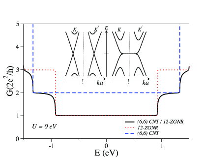
i) Carbon nanotubes are rolled-up cylinders of graphene Iijima (1991). Their electronic properties can be approximately derived from the graphene band structure by imposing the Born-von Karman boundary condition R.Saito et al. (1998), and depending on their geometry, can behave as metals or semiconductors Hamada et al. (1992); Dresselhaus (1996). In this work, we focus in armchair carbon nanotubes that correspond to the configuration with no ’twist’ in the graphene rolling, with an armchair shape of the cross section along the circumference R.Saito et al. (1998). Armchair nanotubes are denoted by , being 2 the number of carbon atoms at the CNT circumference; they are one-dimensional metals with two inequivalent Fermi points in the Brillouin zone, reminiscent of the graphene Dirac points (See inset of Fig. 2).
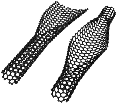
ii) Carbon nanoribbons are obtained by cutting graphene in the form of a quasi-one-dimensional stripe. The electronic properties of GNR strongly depend on the atomic edge termination. There are two basic shapes for graphene edges, armchair and zigzag M.Fujita et al. (1996). The GNR electronic properties can be derived from the graphene band structure by imposing the appropriate boundary conditions Brey and Fertig (2006). Armchair GNR can be either metallic or semiconducting depending of their width, whereas for the zigzag GNR (ZGNR) two-fold degenerated flat bands lie at the Fermi energy. These bands are associated with edge states Brey and Fertig (2006) and their dispersionless character favors an insulating antiferromagnetic ground state, with opposite magnetization at the edges M.Fujita et al. (1996); Fernández-Rossier (2008); Son et al. (2006); Pisani et al. (2007); F.Muñoz-Rojas et al. (2009). Zigzag graphene nanoribbons are obtained by unrolling an armchair CNT, see Fig. 1. The ZGNR width is defined by the number of zigzag rows in the unit cell; the usual notation for such ribbon is -ZGNR.
In this work we study partially unzipped carbon nanotubes, such as those shown in Fig. 1, which are equivalent to a combination of carbon nanotubes and graphene nanoribbons. In what follows, we focus in armchair carbon nanotubes and the derived graphene zigzag nanoribbons.
Model Hamiltonian and transport calculation. We describe the motion of carriers between carbon orbitals with a single first-neighbor hopping parameter . The electronic repulsion is included within the Hubbard model, which we solve in the mean field approximation. For eV and the Hubbard term in the range 1.5 eV 3 eV, this approach describes adequately the main features of the ab initio calculations Fernández-Rossier and Palacios (2007); Fernández-Rossier (2008) around the Fermi energy of graphene nanoribbons. The Hamiltonian reads
| (1) |
where () is a creation (annihilation) operator at atom () of a electron with spin . We consider that the effect of the unzipping is to cut the hopping between the carbon atoms where the opening occurs, and we assume that unzipping does not modify the hopping parameter between the other carbon atoms, which we set to eV. This Hamiltonian depends on the electronic occupation and has to be solved selfconsistently López Sancho et al. (2001).
As the systems lack translational invariance, we follow a Green function (GF) approach to calculate the electronic and transport properties Chico et al. (1996); Nardelli (1999). To this purpose, we divide the system into three parts, namely a central region connected to the right and left leads. The Hamiltonian can thus be written as
| (2) |
where , , and are the Hamiltonians of the central portion, left and right leads respectively, and , are the hoppings from the left and right lead to the central region . The GF of the latter is
| (3) |
where is the selfenergy due to lead , and is the GF of the semiinfinite lead .
In a zero bias approximation, the Landauer conductance is given by
| (4) |
is the transmission function, that can be obtained from the GFs of the central part and the leads:
| (5) |
where describes the coupling of the central region to lead . For a single junction, the left and right electrodes are connected directly, so in Eq. 5 is just the GF of the interface between the left and right lead, .
Results. In Fig. 2 we show the conductance of a single (6,6) CNT/12-ZGNR junction, as the one depicted in the upper panel of Fig. 1, for noninteracting electrons (). As a reference, we show in dashed and dotted lines the conductances of the perfect infinite carbon nanotube and nanoribbon. Around zero energy, the conductance of the junction is equal to that of the perfect nanoribbon, demonstrating that the (6,6) CNT acts as a transparent contact for the 12-ZGNR. Assuming left to right conduction, the ZGNR only has the channel open to transport and it is completely transparent to states from the corresponding valley of the CNT. This indicates that backscattering is practically zero in the device and the conductance in this energy range is set by the ribbon, which acts as a valley filter for the carbon nanotube. Our numerical results show that states from the valley of the CNT cannot transverse the junction. At higher energies, more channels open in the ribbon, so the conductance now is limited by that of the (6,6) nanotube: here, the ribbon is acting as a transparent contact for the carbon nanotube, and transport from both valleys is allowed. Calculations with larger systems, such as a (18,18) CNT/36-ZGNR (not shown here) yield similar results, with the obvious increase in the number of channels at energies closer to the Fermi level. We have also investigated the narrowing of the ribbon part, such as a (6,6) CNT/10-ZGNR, or a (18,18)/32-ZGNR, finding that the effect is robust against the precise form of the CNT/ZGNR junction.


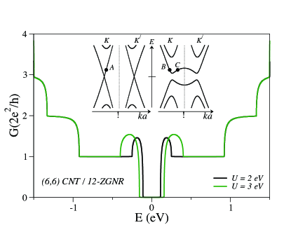
As discussed above, the interaction between electrons changes dramatically the band structure of graphene nanoribbons near the Fermi energy. In the following we analyze how the interactions modify the low energy transport properties. Fig. 3 shows the effect of electron-electron interactions in the conductance of the (6,6)CNT/12-ZGNR junction for eV and eV. The inset shows the bandstructure for the (6,6)CNT and for the 12-ZGNR for an interaction eV. For CNTs the Hubbard interaction does not modify the magnetic moments on the carbon atoms, so the effect of is just a rigid shift of the electronic structure. In the case of ZGNR the interaction orders ferromagnetically the most external atoms at each edge, and the magnetic moments on opposite edges couple antiferromagnetically. Magnetic order induces dispersion of the edge bands along the edge direction, opening a gap at the center of the band structure that increases with the value of the interaction . The states with opposite spin orientation are degenerated, but the edge bands with opposite spin correspond to states located at opposite edges. The many body-induced gap in ZGNR precludes transport near the Fermi energy. Above the gap, there is a region of enhanced conductance with respect to the non-interacting case. This occurs because the dispersion of the edge states, induced by the the electron electron interaction, opens a new electronic channel near each Dirac point of the ZGNR, as for example at point C in the inset of Fig. 3. Besides transmission from to valleys observed in the non-interacting case, now a state A in the CNT valley can be transmitted into state of the ZGNR at the same valley, giving an enhanced conductance. The width of this bump in the conductance is proportional to the midband gap and increases with . The state C is a edge state and for opposite spin orientations the wavefunction of this state is localized in opposite edges. Therefore the excess of current with respect to the noninteracting case (bump regions of Fig. 3) is localized at the edges and with opposite spin polarization. Above this energy region there is an energy interval where the conductance gets the value , and valley filtering occurs, as explained for the non-interacting case. This energy interval is around 0.6 eV for eV, making it possible the observation of this filtering in carbon nanotubes. Above this interval, the conductance values are quite similar to the non-interacting cases, demonstrating the high transparency of armchair CNTs for ZGNR and viceversa. The application of a magnetic field makes the ZGNR ferromagnetic and metallic F.Muñoz-Rojas et al. (2009). The magnetic field closes the midgap, opening new channels at low energies and giving rise to a large magnetoresistance. We propose that a single unzipped carbon nanotube is by itself a device featuring 100 % magnetoresistance.

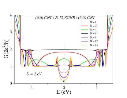
We have also explored the properties of double junction systems, such as the one depicted in Fig. 1 (right), an infinite armchair (6,6) nanotube open in its central part making a ZGNR. We denote this structure as (6,6) CNT/N 12-ZGNR/(6,6) CNT, where N is the number of unit cells in the nanoribbon. The transparency of the nanotube contacts is evident in Fig. 4: the transmission through the central ribbon part is higher that in an infinite ribbon for the smaller sizes, and slowly decays to the zero limit value in the gap with increasing ribbon size. Other combinations, such a CNT quantum dot with ribbon contacts can be envisioned, expanding the possibilities of carbon electronics, in analogy to the quantum dot and superlattice structures proposed for carbon nanotubes L.Chico et al. (1998); Jaskólski and Chico (2005).
In summary, we propose a new class of carbon nanostructures based on unzipped nanotubes, which actually consist of mixed carbon nanotube/nanoribbon systems. We have found that ribbons from unzipped tubes behave as completely transparent contacts for the parent tubes, and viceversa. Our results demonstrate that partially unzipped carbon nanotubes are by themselves magnetoresistive devices, with a large value of the magnetoresistance. Furthermore, carbon nanoribbons act as valley filters for carbon nanotubes; this behavior is robust with respect to the inclusion of electron-electron interaction, opening the possibility of exploiting the valley degree of freedom in a new class of carbon-based nanodevices.
This work has been partially supported by the Spanish DGES under grants MAT2006-06242 and MAT2006-03741 and Spanish CSIC under grant PI 200860I048.
References
- K.S.Novoselov et al. (2004) K.S.Novoselov, A.K.Geim, S.V.Mozorov, D.Jiang, Y.Zhang, S.V.Dubonos, I.V.Gregorieva, and A.A.Firsov, Science 306, 666 (2004).
- K.S.Novoselov et al. (2005) K.S.Novoselov, D.Jiang, T.Booth, V. Khotkevich, S. M. Morozov, and A.K.Geim, Nature 438, 197 (2005).
- Zhang et al. (2005) Y. Zhang, Y.-W. Tan, H. L. Stormer, and P. Kim, Nature 438, 201 (2005).
- Castro-Neto et al. (2009) A. H. Castro-Neto, F.Guinea, N.M.R.Peres, K.S.Novoselov, and A.K.Geim, Rev. Mod. Phys. 81, 109 (2009).
- A.F.Morpurgo and F.Guinea (2006) A.F.Morpurgo and F.Guinea, Phys. Rev. Lett. 97, 196804 (2006).
- Rycerz et al. (2007) A. Rycerz, J. Tworzydło, and C. W. Beenakker, Nature Phys. 3, 172 (2007).
- Berger et al. (2006) C. Berger, Z. Song, X. Wu, N. Brown, C. Naud, D. Mayou, T. Li, J. Hass, A. N. Marchenkov, E. H. Conrad, et al., Science 312, 1191 (2006).
- Iyengar et al. (2008) A. Iyengar, T. Luo, H. A. Fertig, and L. Brey, Phys.Rev.B 78, 235411 (2008).
- Han et al. (2007) M. Y. Han, B. Özyilmaz, Y. Zhang, and P. Kim, Physical Review Letters 98, 206805 (pages 4) (2007), URL http://link.aps.org/abstract/PRL/v98/e206805.
- Özyilmaz et al. (2007) B. Özyilmaz, P. Jarillo-Herrero, D. Efetov, D. A. Abanin, L. S. Levitov, and P. Kim, Phys. Rev. Lett. 99, 166804 (2007).
- Schniepp et al. (2006) H. C. Schniepp, J.-L. Li, M. J. McAllister, H. Sai, M. Herrera-Alonso, D. H. Adamson, R. K. Prud’homme, R. Car, D. A. Saville, and I. A. Aksay, J. Phys. Chem. B 110, 8535 (2006).
- Li et al. (2008) X. Li, X. Wang, L. Zhang, S. Lee, and H. Dai, Science 319, 1229 (2008).
- Yang et al. (2008) X. Yang, X. Dou, A. Rouhanipour, L. Zhi, H. J. Rader, and K. Mullen, J. Am. Chem. Soc. 130, 4126 (2008).
- Campos-Delgado et al. (2008) J. Campos-Delgado, J. M. Romo-Herrera, X. Jia, D. A. Cullen, H. Muramatsu, Y. A. Kim, T. Hayashi, Z. Ren, D. J. Smith, Y. Okuno, et al., Nano Lett. 8, 2773 (2008).
- Kosynkin et al. (2009) D. V. Kosynkin, A. Higginbotham, A. Sinitskii, J. R. Lomeda, A. Dimiev, B. K. Price, and J. M. Tour, Nature 458, 872 (2009).
- Jiao et al. (2009) L. Jiao, L. Zhang, X. Wang, G. Diankov, and H. Dai, Nature 458, 877 (2009).
- Iijima (1991) S. Iijima, Nature 354, 56 (1991).
- R.Saito et al. (1998) R.Saito, G.Dresselhaus, and M.S.Dresselhaus, Physical Properties of Carbon Nanotubes (Imperial College, London, 1998).
- Hamada et al. (1992) N. Hamada, S.-I. Sawada, and A. Oshiyama, Phys. Rev. Lett. 68, 1579 (1992).
- Dresselhaus (1996) M. Dresselhaus, Physics World 9, 18 (1996).
- M.Fujita et al. (1996) M.Fujita, K. Wakabayashi, K.Nakada, and K.Kusakabe, J.Phys. Soc. Jpn. 65, 1920 (1996).
- Brey and Fertig (2006) L. Brey and H. Fertig, Phys. Rev. B 73, 325411 (2006).
- Fernández-Rossier (2008) J. Fernández-Rossier, Phys. Rev. B 77, 075430 (2008).
- Son et al. (2006) Y. Son, M. L. Cohen, and S. G. Louie, Phys.Rev.Lett. 97, 216803 (2006).
- Pisani et al. (2007) L. Pisani, J. Chan, B. Montanari, and N. Harrison, Phys. Rev. B 75, 064418 (2007).
- F.Muñoz-Rojas et al. (2009) F.Muñoz-Rojas, J.Fernández-Rossier, and J.J.Palacios, Phys. Rev. Lett. 102, 136810 (2009).
- Fernández-Rossier and Palacios (2007) J. Fernández-Rossier and J. J. Palacios, Phys. Rev. Lett. 99, 177204 (2007).
- López Sancho et al. (2001) M. P. López Sancho, M. C. Muñoz, and L. Chico, Phys. Rev. B 63, 165419 (2001).
- Chico et al. (1996) L. Chico, L. X. Benedict, S. G. Louie, and M. L. Cohen, Phys. Rev. B 54, 2600 (1996).
- Nardelli (1999) M. B. Nardelli, Phys. Rev. B 60, 7828 (1999).
- L.Chico et al. (1998) L.Chico, M.P.López-Sancho, and M. noz, Phys. Rev. Lett. 81, 1278 (1998).
- Jaskólski and Chico (2005) W. Jaskólski and L. Chico, Phys. Rev. B 71, 155405 (2005).