Practical vortex diodes from pinning enhanced YBa2Cu3O7-δ
Abstract
We identify a scalable, practical route to fabricating a superconducting diode. The device relies for its function on the barrier to flux vortex entry being reduced at the substrate interface of a superconducting pinning enhanced YBa2Cu3O7-δ nano-composite film. We show that these composite systems provide a practical route to fabricating a useful superconducting diode and demonstrate the rectification of an alternating current.
pacs:
74.60.Jg, 74.60.Ge, 74.72.BkA Type-II superconducting system where vortices can move more easily forward than backwards constitutes a vortex diode. Such a system will give rise to a superconducting diode when a transport current is applied Krasnov et al. (1997). This type of device exhibits no voltage drop across it until a critical current is reached and the magnitude of this critical current will depend on the direction of current flow, this is the opposite of the behaviour of a semiconductor diode. A practical implementation of such a device could find applications in AC-DC conversion, fault current limiters and superconducting electronics.
Vortex diodes have been demonstrated utilising ratchet effects from asymmetric pinning potentials Wordenweber et al. (2004); Lu et al. (2007); Shalom and Pastoriza (2005); Van de Vondel et al. (2005); Yu et al. (2007) and asymmetric driving potentialsCole et al. (2006). These studies have concentrated on the fundamental interest in these model physical systems and the effects demonstrated have not been compatible with large scale fabrication methods or high currents. Additionally, several workersBroussard and Geballe (1988); Jiang et al. (1994); Jiang and Lobb (1995), notably Jiang et al., have reported superconducting diode-like characteristics in low- superconducting thin films due to surface pinning effects.
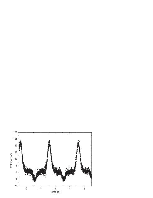
In this letter, we describe the superconducting diode behaviour of the cuprate-superconductor/non-superconducting oxide nano-composites which have recently driven order of magnitude increases in the current carrying capacity of YBa2Cu3O7-δHarrington et al. (2009); Maiorov et al. (2009); Mele et al. (2008)(YBCO). Figure 1 shows the rectification of a low-frequency AC signal using a sample investigated in this paper, a YBa2Cu3O7-δ + RE3TaO7 film, a standard pinning enhanced cuprate material.

In YBa2Cu3O7-δ one of the most prominent features in the dependence of on the orientation of magnetic field is the maximum found when the field is applied parallel to the a-b planes. This maximum, often termed the ‘intrinsic’ pinning peak, was discovered early in the exploitation of the cuprate superconductorsRoas et al. (1990). The peak is a result of a complex mixture of contributions including surface pinning, the Ginzburg-Landau anisotropy of the materialCivale et al. (2004), the layered structure of the materialNishizaki et al. (1991); Tachiki and Takahashi (1989) and in-plane oriented pinning centresMaiorov et al. (2007). The importance of surface pinning is often neglected although prior work on vicinal films, in which geometrical effects are separated from intrinsic effects, shows that it can be of a magnitude equal to the intrinsic pinning Berghuis et al. (1996).

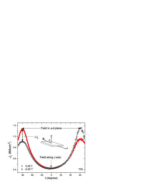
We have experimentally observed, in several different types of pinning-enhanced YBa2Cu3O7-δ [YBa2Cu3O7-δ + BaZrO3, YBa2Cu3O7-δ + RE3TaO7 and REaREbBa2Cu3O7-δ], that where the magnetic field angular dependence of was measured, maxima arising from opposite magnetic field directions can be significantly different. One peak characteristically exhibits a reduced maximum, as shown in figure 2; a flattened maximum; or even a local minimum superimposed on the ‘intrinsic peak’. From the experimental geometry we have determined that the suppressed maximum corresponds to entry of vortices at the film-substrate interface, conversely the larger peak arises from entry of vortices at the free surface.
This effect arises for in-plane fields because the strong demagnetising factor associated with the large anisotropy of a thin film is eliminated when magnetic field is applied parallel to the film. In this geometry the difference between the surface barriers at the two interfaces becomes apparent. Wherever there is an abrupt change in superconducting properties over a short distanceCampbell and Evetts (1972) a barrier to vortex motion arises. The barriers to vortex motion at the surface of a superconductor are described by the Bean-Livingston modelBean and Livingston (1964). Of the entry and escape barriers the entry barrier is largerClem (1974), they are differently affected by surface imperfections. Vodolazov et al.Vodolazov and Peeters (2005) note that an asymmetry in critical current for reversed Lorentz force will arise wherever surface pinning is significant. The asymmetry is most significant at small fields where the surface pinning barrier is large compared to the pinning force density on the vortex lattice. Kumar et al. have experimentally demonstrated that the surface barrier can be greatly reduced by grading the superconductor interfaceKumar et al. (1994).

On the assumption that the effect seen in our films was due to a graded interface reducing surface pinning at the film-substrate interface, a number of rare earth tantalate (RTO) doped films were preparedHarrington et al. (2009) in which growth conditions were chosen so as to encourage disorder at the film-substrate interface. This involved using fast deposition rates and low growth temperatures to slow the assembly of the pinning enhanced phase. The resulting films had normal transition temperatures ( 91 K) but due to the non-optimum growth conditions somewhat reduced self-field critical currents compared to that of standard RTO + YBa2Cu3O7-δ thin films. YBa2Cu3O7-δ + 5 mol % Yb3TaO7 composition films were found to give the largest anisotropy and it is data from such a film that we present in this letter. Measurements were performed using a two-axis goniometer mounted in an 8 T magnetHerzog and Evetts (1994), on a 1 mm long 500 nm x 90 m track patterned using standard photolithographic techniques. A four terminal measurement was used to obtain characteristics from which critical current values were determined using a voltage criterion of 0.75 V.
Figure 2 clearly shows the large difference in critical current when the Lorentz force is reversed, for an in-plane magnetic field. It was also found that a reversal of the measurement current direction produced the equivalent anisotropy.
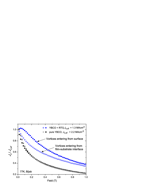
In figure 3 we show the striking difference between the behaviour of the interface engineered YBa2Cu3O7-δ + Yb3TaO7 film and a reference YBa2Cu3O7-δ sample grown under standard conditions. It is apparent, that while the pure YBa2Cu3O7-δ film does exhibit some surface pinning anisotropy the effect is opposite to, and much smaller than, that seen in the interface engineered film. We conclude that the small effect seen in the pure YBa2Cu3O7-δ film is due to the free surface being slightly rougher than the film-substrate interface.

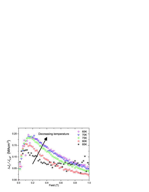
In figure 4 the magnitude of the difference in the surface pinning at the two interfaces increases with decreasing measurement temperature. The figure also highlights the decreasing anisotropy with increasing field for all temperatures measured. The anisotropy extends beyond 1 T with a peak being observed around 0.18 T. An explanation involving surface pinning is consistent with the observed behaviour for several reasons: the effect disappears in high fields, consistent with the Bean-Livingston modelBean and Livingston (1964), unlike vortex channelling effects which are field independent Durrell et al. (2003, 2004); no asymmetric bulk pinning is present in the films; and the films have large critical currents meaning that channelling at poor growth-grain boundaries is not likely. Further, the sample does not exhibit the c axis peak in which occurs when nanorods are presentGoyal et al. (2005), suggesting that channelling along nanorod arrays is unlikely to be present.
In conclusion we have demonstrated a superconducting diode with a 25% variation in critical current in pinning enhanced YBa2Cu3O7-δ nano-composite films. We suggest that this is a result of disorder that occurs in these mixed oxide immiscible systems, meaning large area devices can be reliably created through spontaneous interface grading. We expect that a better understanding of how to control the film-substrate interface in pinning-enhanced YBa2Cu3O7-δ will permit further improvement of these diode-like properties. Further, the existence of this diode effect means that it is necessary to measure both in-plane peaks and avoid commutating measurements of voltage when studying the angular critical current dependence of such nano-composite films.
The authors would like to thank J. R. Clem and M. G. Blamire for helpful discussions. This work was supported by the Engineering and Physical Science Research Council [grant numbers EP/C011554/1, EP/C011546/1] and the EU Marie Curie Excellence programme [grant number MEXT-CT-2004-014156].
References
- Krasnov et al. (1997) V. M. Krasnov, V. A. Oboznov, and N. F. Pedersen, Physical Review B 55, 14486 (1997).
- Wordenweber et al. (2004) R. Wordenweber, P. Dymashevski, and V. R. Misko, Physical Review B 69, 184504 (2004).
- Lu et al. (2007) Q. M. Lu, C. J. O. Reichhardt, and C. Reichhardt, Physical Review B 75, 054502 (2007).
- Shalom and Pastoriza (2005) D. E. Shalom and H. Pastoriza, Physical Review Letters 94, 177001 (2005).
- Van de Vondel et al. (2005) J. Van de Vondel, C. C. D. Silva, B. Y. Zhu, M. Morelle, and V. V. Moshchalkov, Physical Review Letters 94, 057003 (2005).
- Yu et al. (2007) K. Yu, T. W. Heitmann, C. Song, M. P. Defeo, B. L. T. Plourde, M. B. S. Hesselberth, and P. H. Kes, Physical Review B 76, 220507 (2007).
- Cole et al. (2006) D. Cole, S. Bending, S. Savel’ev, A. Grigorenko, T. Tamegai, and F. Nori, Nature Materials 5, 305 (2006).
- Broussard and Geballe (1988) P. R. Broussard and T. H. Geballe, Physical Review B 37, 68 (1988).
- Jiang et al. (1994) X. G. Jiang, P. J. Connonlly, S. J. Hagen, and C. J. Lobb, Physical Review B 49, 9244 (1994).
- Jiang and Lobb (1995) X. G. Jiang and C. J. Lobb, Journal Of Low Temperature Physics 100, 515 (1995).
- Harrington et al. (2009) S. A. Harrington, J. H. Durrell, B. Maiorov, H. Wang, S. C. Wimbush, A. Kursumovic, J. H. Lee, and J. L. MacManus-Driscoll, Superconductor Science & Technology 22, 022001 (2009).
- Maiorov et al. (2009) B. Maiorov, S. A. Baily, H. Zhou, O. Ugurlu, J. A. Kennison, P. C. Dowden, T. G. Holesinger, S. R. Foltyn, and L. Civale, Nature Materials 8, 398-404 (2009).
- Mele et al. (2008) P. Mele, K. Matsumoto, A. Ichinose, M. Mukaida, Y. Yoshida, S. Horii, and R. Kita, Superconductor Science & Technology 21, 125017 (2008).
- Roas et al. (1990) B. Roas, L. Schultz, and G. Saemannishenko, Phys. Rev. Lett. 64, 479 (1990).
- Civale et al. (2004) L. Civale, B. Maiorov, A. Serquis, J. O. Willis, J. Y. Coulter, H. Wang, Q. X. Jia, P. N. Arendt, J. L. MacManus-Driscoll, M. P. Maley, and S. R. Foltyn , Applied Physics Letters 84, 2121 (2004).
- Nishizaki et al. (1991) T. Nishizaki, T. Aomine, I. Fujii, K. Yamamoto, S. Yoshii, T. Terashima, and Y. Bando, Physica C 185, 2259 (1991).
- Tachiki and Takahashi (1989) M. Tachiki and S. Takahashi, Solid State Communications 70, 291 (1989).
- Maiorov et al. (2007) B. Maiorov, Q. X. Jia, H. Zhou, H. Wang, Y. Li, A. Kursumovic, J. L. MacManus-Driscoll, T. J. Haugan, P. N. Barnes, S. R. Foltyn, and L. Civale, IEEE Transactions on Applied Superconductivity 17, 3697 (2007).
- Berghuis et al. (1996) P. Berghuis, F. Baudenbacher, R. Herzog, R. Somekh, A. M. Campbell, J. E. Evetts, and G. Wirth, in Proc. 8th IWCC in Superconductors, edited by T. M. Matsushita and K. Yamafuji (World Scientific, Singapore, 1996), p. 247.
- Campbell and Evetts (1972) A. Campbell and J. Evetts, Advances in Physics 50, 1249 (1972).
- Bean and Livingston (1964) C. P. Bean and J. D. Livingston, Physics Review Letters 12, 14 (1964).
- Clem (1974) J. R. Clem, in Low Temperature Physics - LT13, edited by K. D. Timmerhaus, W. J. O’Sullivan, and E. F. Hammel (1974), vol. 3, pp. 102–106.
- Vodolazov and Peeters (2005) D. Y. Vodolazov and F. M. Peeters, Physical Review B 72, 172508 (2005).
- Kumar et al. (1994) D. D. Kumar, M. G. Blamire, R. Doyle, A. M. Campbell, and J. E. Evetts, Journal Of Applied Physics 76, 2361 (1994).
- Herzog and Evetts (1994) R. Herzog and J. E. Evetts, Review Of Scientific Instruments 65, 3574 (1994).
- Durrell et al. (2003) J. H. Durrell, M. J. Hogg, F. Kahlmann, Z. H. Barber, M. G. Blamire, and J. E. Evetts, Physical Review Letters 90, 247006 (2003).
- Durrell et al. (2004) J. H. Durrell, G. Burnell, Z. H. Barber, M. G. Blamire, and J. E. Evetts, Physical Review B 70, 214508 (2004).
- Goyal et al. (2005) A. Goyal, S. Kang, K. J. Leonard, P. M. Martin, A. A. Gapud, M. Varela, M. Paranthaman, A. O. Ijaduola, E. D. Specht, J. R. Thompson, D. K. Christen, S. J. Pennycook and F. A. List, Superconductor Science & Technology 18, 1533 (2005).