Current address: ]Department of Physics, University of California at Berkeley, USA
Indication of a non-magnetic surface layer on a magnetic single crystal
Abstract
The structural and electronic properties of the surfaces of Sm(0001) and Eu/Gd(0001) were studied by scanning tunneling microscopy and spectroscopy at temperatures between 10 and 110 K. In both systems, an unoccupied surface state is observed that exhibits a temperature-dependent splitting into two states for Eu/Gd(0001), while it is unsplit on Sm(0001). This strongly indicates that the divalent outermost surface layer of Sm(0001) is non-magnetic despite the antiferromagnetic trivalent Sm substrate. These findings open new opportunities for magnetic studies of ultra-thin Sm films.
pacs:
68.37.Ef, 73.20.At, 75.70.Ak, 75.70.RfThe magnetic properties of trivalent lanthanide (Ln) metal surfaces have been the subject of some controversy in the past. For Gd(0001), e.g., the possibility of an enhanced surface Curie temperature () and an orientation of surface magnetization different from the bulk has been debated Dowben and McIllroy (1997). Some of this behavior could be due to the magnetic exchange splitting of surface states that does not follow a simple Stoner-like behavior but is also influenced by spin mixing and short-range magnetic order at higher temperatures Bode et al. (1999); Wegner et al. (2006a). More recent experiments have convincingly shown that the magnetic properties of most Ln-metal surfaces are essentially the same as in the bulk C. S. Arnold and D. P. Pappas (2000); Maiti et al. (2002).
The situation is quite different for Sm metal, where a strong deviation of surface from bulk magnetism can be expected due to the well-known surface valence transition G. K. Wertheim and G. Crecelius (1978). While Sm in the bulk is trivalent and magnetic with an ground state , the reduced coordination at the surface leads to a valence change to divalent Sm with a non-magnetic ground state G. K. Wertheim and G. Crecelius (1978); Johansson (1979). This valence change is accompanied by a dramatic increase of the ionic radius by 22 % as well as a reconstruction of the Sm(0001) surface Stenborg et al. (1989); Lundgren et al. (2002). Since Sm metal orders antiferromagnetically (AFM) in the bulk below Koehler and Moon (1972), the question arises whether the outermost Sm(0001) surface layer is magnetic or non-magnetic below .
The present study shows that Sm(0001) exhibits a previously unnoticed d-like surface state that allows to address this question by studying its magnetic exchange splitting via scanning tunneling spectroscopy (STS) as a function of (). For comparison, a monolayer (ML) of Eu on Gd(0001) was studied that exhibits an analogous surface reconstruction but differs in its local moments: both Eu and Gd have non-vanishing moments () and couple ferromagnetically (FM) below Arenholz et al. (1998); Dedkov et al. (2006). The outermost divalent Eu layer exhibits also a d-like surface state. While we observe a -dependent splitting of the Eu/Gd(0001) surface state, the analogous surface state on Sm(0001) consists of a single peak. This strongly indicates that the outermost surface layer of Sm metal is non-magnetic.
The experiments were performed in ultrahigh vacuum (base pressure ) with a home-built low- STM operated between 10 and 110 K Bauer et al. (2002). All Ln-metal films were deposited in situ by electron-beam evaporation of 99.99% pure metals from a Ta crucible onto a clean W(110) single crystal kept at room temperature (RT). The 10-ML-thick Sm films were not annealed upon deposition, since RT deposition readily leads to smooth films Lundgren et al. (2002). For Eu/Gd(0001), first a 30-ML-thick Gd(0001) film was grown on W(110) and annealed to obtain a smooth, crystalline film Rehbein et al. (2003), followed by deposition of about 1 ML Eu on the Gd film kept at RT. The samples were then transferred in UHV to the cryogenic STM. STS spectra were recorded with fixed tip position and switched-off feedback loop using standard lock-in techniques (modulation amplitude: 1 mV (rms), modulation frequency: ). As is well known, the differential conductivity, , is approximately proportional to the local density of states of the surface ( tunneling current; sample bias voltage).
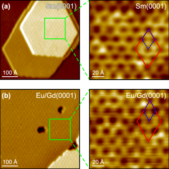
Fig. 1(a) shows the topography of a 10-ML Sm(0001) film. The surface is atomically flat with ML-high terraces. The close-up view on a terrace shows the hexagonal Moiré pattern of the well-known surface reconstruction caused by the larger radius of divalent Sm surface atoms. The structure was first identified by low-energy electron diffraction as a reconstruction (leading to a unit-cell size of 1.81 nm) Stenborg et al. (1989). A recent combined x-ray diffraction, STM, and density-functional-theory study showed that the reconstruction is actually incommensurate with an approximate unit cell [red diamond in Fig. 1(a)] Lundgren et al. (2002). Thus, the Moiré pattern corresponds to an effective unit cell with a size of 2.00 nm; we observe a size of [blue dashed diamond in Fig. 1(a)], in good agreement with Ref. Lundgren et al., 2002.

In comparison, Fig. 1(b) shows STM images of 1 ML Eu/Gd(0001), with a Moiré pattern very similar to that of Sm(0001). Previously, two different commensurate surface reconstructions have been reported, and Arenholz et al. (1997, 1998), which would lead to apparent Moiré-pattern sizes of 2.18 nm and 1.82 nm, respectively 111Dedkov et al. reported a reconstruction, supposedly due to a different sample-preparation procedure, see Ref. Dedkov et al., 2006.. We find a size of (blue diamond), very similar to the Sm(0001) reconstruction. This Moiré pattern is not compatible within the limits of error with either one of the reported reconstructions. We suggest that the Eu monolayer is also best described by an reconstruction (red diamond), with an effective Moiré pattern (blue dashed diamond). This underlines that Sm(0001) and Eu/Gd(0001) are well suited for a direct comparison, because both their surface reconstructions are identical and the lattice constants of the hexagonal bulk basal planes are the same for Sm(0001) and Gd(0001) () Lide (2004).
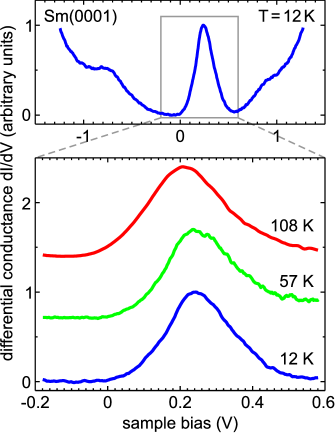
The STS spectrum of Sm(0001) (Fig. 2) is dominated by a narrow resonance at 0.25 meV above , independent of the tip position on the reconstruction pattern. At this energy, all trivalent Ln metals exhibit a gap in the center of the projected surface band structure, i.e. around the point of the Brillouin zone (BZ) Kurz et al. (2002); Wegner et al. (2006b). We can therefore rule out that this strong spectral feature is caused by a bulk band. Instead, it is reminiscent of the Tamm-like surface states with symmetry observed for other Ln-metal surfaces Bode et al. (1998, 1999); Bauer et al. (2002); Wegner et al. (2006c). We conclude that the observed peak stems from a surface state of the divalent Sm(0001) surface. Note that a single peak is observed in the present case, quite similar to the surface states on non-magnetic trivalent La(0001) and Lu(0001). Furthermore, STS at various shows – apart from the expected slight increase of width with increasing – no significant change of this peak, particularly no indication of magnetic exchange splitting (see below) 222The slight shift of the STS spectrum at 108 K is most likely a -induced artifact of the measurements..
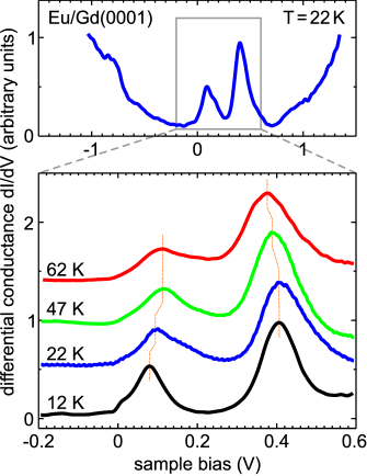
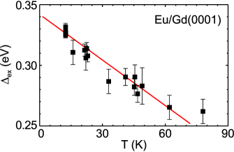
In contrast, the STS spectrum of 1 ML Eu/Gd(0001) (Fig. 3) is dominated by two peaks at about 0.1 eV and 0.4 eV above , respectively, again showing no dependence on tip position. The two peaks are also within the gap in the center of the projected surface BZ of Gd(0001), reminiscent of the exchange-split surface states of magnetic trivalent Ln metals Wegner et al. (2006c). In order to check this, we studied the -dependence of the peak positions. With increasing , the peak at 0.1 eV clearly shifts to higher energies, while the peak at 0.4 eV shifts down towards , reflecting a decrease of the energy separation of the two peaks with increasing . This strongly supports an interpretation on the basis of magnetic exchange splitting into two (majority- and minority-spin) components separated by . Fig. 4 displays as a function of . Within the studied temperature range, decreases approximately linearly with increasing , with a maximum splitting . Extrapolation towards higher indicates that the splitting would vanish at , which is close to the of the FM Gd substrate. We note, however, that the exchange splitting is not expected to decrease linearly with at higher , and it might not decrease to zero either Wegner et al. (2006a).


To summarize the observations, only one peak can be observed in the STS spectra of Sm(0001), with no significant dependence, whereas the Eu/Gd(0001) surface exhibits two peaks, with a separation that decreases with increasing . All peaks lie within a local band gap in the center of the projected surface BZs of Sm(0001) and Gd(0001), respectively. We therefore interpret these resonances as signatures of an unoccupied surface state of the divalent Ln-metal surface layers. Similar to the scenario of trivalent Ln metals, the narrow, almost Lorentzian-like peak shapes indicate weak parallel dispersions and hence a relatively high spatial localization of these surface states Bauer et al. (2002); Wegner et al. (2006b).
The exchange splitting of the Eu/Gd(0001) surface state is caused by FM coupling of the Eu surface layer to the Gd(0001) substrate. The maximum exchange splitting of 0.34 eV is about half as large as that observed for the surface state on pristine Gd(0001), although both surfaces have a spin . This can be understood by a reduced spin polarization of the Eu layer relative to the Gd substrate Arenholz et al. (1998); Dedkov et al. (2006). Additionally, the larger nearest-neighbor distance of Eu-surface atoms should lead to a smaller interatomic overlap, which should further reduce the exchange splitting.
In previous studies it was shown that the ground-state exchange splitting of electronic bands in the Ln metals does not depend on the total magnetic moment. Instead, it scales almost linearly with the spin Schüßler-Langeheine et al. (2000); Weschke and Kaindl (2001); Wegner et al. (2006c). From the measured exchange splitting of Eu/Gd(0001), we can estimate the expected splitting for (the spin of divalent Sm) to about 0.29 eV. The Sm spectra in Fig. 2 do not allow for such a large splitting. One may argue that the exchange splitting of Sm might be much smaller, because bulk Sm is AFM. However, within each of the closed-packed basal planes of the Sm(0001) crystal, the atomic moments are FM coupled, leading to a local spin polarization of the subsurface layer Koehler and Moon (1972). Note that a significant exchange splitting has also been observed for the surface state on the complex AFM Nd(0001) Wegner et al. (2006a).
We also studied the possibility of describing the STS spectrum of Sm(0001) by two unresolved components, since the single peak in the Sm spectrum has a width of (FWHM) at 12 K, i.e., it is about twice as broad as the peaks in the Eu/Gd(0001) case. Satisfactory fits could only be obtained for a peak separation of less than 0.10 eV, i.e. less than half the exchange splitting expected for a magnetic divalent Sm surface. An argument against magnetic splitting is given by the fact that the width of the single STS peak increases slightly to at 108 K by thermal effects, while it should decrease towards if magnetic splitting would play a role. The observed increase in peak width is fully compatible with expectations from both STS data for other Ln-metal surface states and theory Rehbein et al. (2003); Wegner et al. (2006a); Skriver and Mertig (1990). Note also that a doubling of the width of the STS peak can be understood if we consider that the spin is not well-defined for the non-magnetic Sm surface state when an excited electron can scatter into both majority- and minority-band states of the bulk electronic structure, whereas in case of Eu/Gd, the (well-defined) spin is conserved. For Sm, this would double the number of available final states and in turn the inverse lifetime (proportional to the peak width). All these considerations support our conclusion that the topmost divalent Sm surface layer on Sm(0001) is non-magnetic despite the magnetically ordered trivalent Sm substrate.

The described observations and conclusions should open new opportunities for atomic-scale local probe studies of mixed-valent ultra-thin Sm films (see Ref. Nakayama et al. (2006)). Through the absence or presence of a -dependent exchange splitting, it should be possible to determine the valence state in Sm films. Photoemission experiments on ultra-thin Sm films revealed such valence changes as a function of nominal film thickness that might now be analyzed with high lateral resolution by low- STM/STS. It is expected that particularly the combination of high energy resolution with the high lateral resolution of STS will lead to new insight in the topic of mixed valency.
This work was supported by the Deutsche Forschungsgemeinschaft (DFG), projects KA 564/10-1 and STA 413/3-1. D.W. is grateful to the Alexander von Humboldt Foundation for financial support.
References
- Dowben and McIllroy (1997) P. A. Dowben and D. N. McIllroy, in Handbook on the Physics and Chemistry of Rare Earths, edited by K. A. Gschneidner, Jr. and L. Eyring (Elsevier, 1997), vol. 24.
- Bode et al. (1999) M. Bode, M. Getzlaff, A. Kubetzka, R. Pascal, O. Pietzsch, and R. Wiesendanger, Phys. Rev. Lett. 83, 3017 (1999).
- Wegner et al. (2006a) D. Wegner, A. Bauer, A. Rehbein, and G. Kaindl, Jap. J. Appl. Phys. 45, 1941 (2006a).
- C. S. Arnold and D. P. Pappas (2000) C. S. Arnold and D. P. Pappas, Phys. Rev. Lett. 85, 5202 (2000).
- Maiti et al. (2002) K. Maiti, M. C. Malagoli, A. Dallmeyer, and C. Carbone, Phys. Rev. Lett. 88, 167205 (2002).
- G. K. Wertheim and G. Crecelius (1978) G. K. Wertheim and G. Crecelius, Phys. Rev. Lett. 40, 813 (1978).
- Johansson (1979) B. Johansson, Phys. Rev. B 19, 6615 (1979).
- Stenborg et al. (1989) A. Stenborg, J. N. Andersen, O. Björneholm, A. Nilsson, and N. Mårtensson, Phys. Rev. Lett. 63, 187 (1989).
- Lundgren et al. (2002) E. Lundgren, J. N. Andersen, R. Nyholm, X. Torrelles, J. Rius, A. Delin, A. Grechnev, O. Eriksson, C. Konvicka, M. Schmid, et al., Phys. Rev. Lett. 88, 136102 (2002).
- Koehler and Moon (1972) W. C. Koehler and R. M. Moon, Phys. Rev. Lett. 29, 1468 (1972).
- Arenholz et al. (1998) E. Arenholz, K. Starke, G. Kaindl, and P. J. Jensen, Phys. Rev. Lett. 80, 2221 (1998).
- Dedkov et al. (2006) Y. S. Dedkov, T. Kleissner, E. N. Voloshina, S. Danzenbächer, S. L. Molodtsov, and C. Laubschat, Phys. Rev. B 73, 012402 (2006).
- Bauer et al. (2002) A. Bauer, A. Mühlig, D. Wegner, and G. Kaindl, Phys. Rev. B 65, 75421 (2002).
- Rehbein et al. (2003) A. Rehbein, D. Wegner, G. Kaindl, and A. Bauer, Phys. Rev. B 67, 33403 (2003).
- Arenholz et al. (1997) E. Arenholz, K. Starke, and G. Kaindl, Appl. Phys. Lett. 71, 3430 (1997).
- Lide (2004) D. R. Lide, CRC Handbook of Chemistry and Physics, 85th ed. (CRC Press, Boca Raton, FL, 2004).
- Kurz et al. (2002) P. Kurz, G. Bihlmayer, and S. Blügel, J. Phys. Condens. Matter 14, 6353 (2002).
- Wegner et al. (2006b) D. Wegner, A. Bauer, Y. M. Koroteev, G. Bihlmayer, E. V. Chulkov, P. M. Echenique, and G. Kaindl, Phys. Rev. B 73, 115403 (2006b).
- Bode et al. (1998) M. Bode, M. Getzlaff, S. Heinze, R. Pascal, and R. Wiesendanger, Appl. Phys. A 66, S121 (1998).
- Wegner et al. (2006c) D. Wegner, A. Bauer, and G. Kaindl, Phys. Rev. B 73, 165415 (2006c).
- Schüßler-Langeheine et al. (2000) C. Schüßler-Langeheine, E. Weschke, C. Mazumdar, R. Meier, A. Y. Grigoriev, G. Kaindl, C. Sutter, D. Abernathy, G. Grübel, and M. Richter, Phys. Rev. Lett. 84, 5624 (2000).
- Weschke and Kaindl (2001) E. Weschke and G. Kaindl, J. Phys. Condens. Matter 13, 11133 (2001).
- Skriver and Mertig (1990) H. L. Skriver and I. Mertig, Phys. Rev. B 41, 6553 (1990).
- Nakayama et al. (2006) Y. Nakayama, H. Kondoh, and T. Ohta, Surf. Sci. 600, 2403 (2006).