Determining exciton bandwidth and film microstructure in polythiophene films using linear absorption spectroscopy.
Abstract
We analyze the linear absorption spectrum of regioregular poly(3-hexylthiophene) films spun from a variety of solvents to probe directly the film microstructure and how it depends on processing conditions. We estimate the exciton bandwidth and the percentage of the film composed of aggregates quantitatively using a weakly interacting H-aggregate model. This provides a description of the degree and quality of crystallites within the film and is in turn correlated with thin-film field-effect transistor characteristics.
In thin films, regioregular poly(3-hexylthiophene) (rrP3HT) self-organizes into two-dimensional -stacked lamellar structures McCullough et al. (1993); Sirringhaus et al. (1999). The degree of order within and around these supramolecular structures depends sensitively on polymer characteristics and thin film processing conditions (Kline and McGehee, 2006; Sirringhaus et al., 1999). These in turn greatly affect device performance. Here we use linear absorption spectroscopy as a simple probe of how thin film microstructure varies with processing conditions. The absorption spectrum of rrP3HT thin films can be comprehensively explained using a weakly interacting H-aggregate model Clark et al. (2007); Spano (2005, 2006). This model can be used to dissect the absorption spectrum, providing quantitative estimates not only of the fraction of the film made up of aggregates (recently determined using different methods Moule et al. (2008); Berson et al. (2007)), but also the degree of excitonic coupling within the aggregates, a parameter which is related to average conjugation length and the crystalline quality. Using this information, we obtain an overall description of the microstructure of the films, which we find to be well correlated with thin-film field effect transistor (FET) characteristics.
rrP3HT (Plextronics and Merck) was dissolved in various solvents (Aldrich) at a concentration of 10 gL-1 and spin-coated onto either fused silica spectrocil B or patterned FET substrates. The films were annealed at 100∘C for 1 hr. The FET-patterned substrates were fabricated in a bottom gate, bottom-contact configuration. The gate electrode was a heavily n-doped Si wafer with 200 nm thermally grown SiO2 as dielectric. A Au layer of 15–20 nm was patterned on the substrates as source/drain electrodes with a channel length of 20 m by conventional photolithography. The channel widths were 1 cm. The patterned substrates were treated with hexamethyldisilazane (HMDS). All processing, and I-V measurements were performed in a N2 atmosphere. Absorption measurements were performed in ambient conditions using a HP 8453 uv-vis spectrometer and tapping-mode atomic force microscopy (AFM) measurements were taken using a Digital Instruments Dimension 3100 AFM.
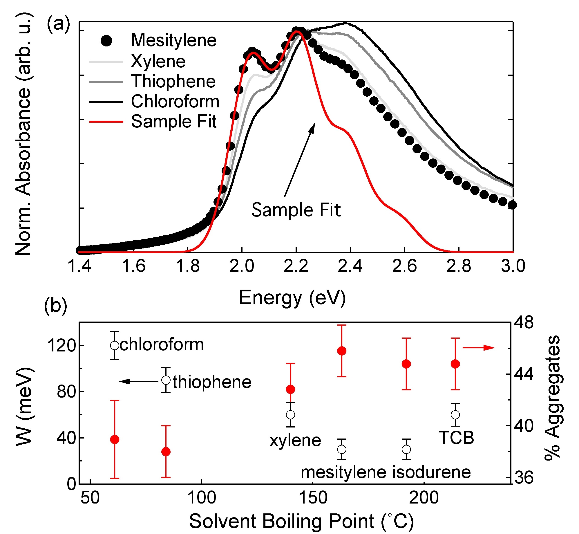
The absorbance spectra of rrP3HT thin films spun from various solvents are shown in Fig. 1 (a). The film absorption spectrum is composed of two parts Clark et al. (2007), a lower energy, dominant part from crystalline regions of the film which form weakly interacting H-aggregate states and a higher energy part due to more disordered chains which form intrachain states. The ratio of the 0–0 and 0–1 peak absorbance is related to the exciton bandwidth of the aggregates, , and the energy of the main oscillator coupled to the electronic transition, , by the following expression (assuming a Huang-Rhys factor of 1 Spano (2005); Clark et al. (2007)):
| (1) |
Using the 0–0/0–1 ratio from Fig. 1, and assuming the C=C symmetric stretch at 0.18 eV dominates the coupling to the electronic transition Louarn et al. (1996), can be estimated. Assuming similar interchain order in the films, is related to the conjugation length and intrachain order. An increase in conjugation length and order will lead to a decrease in (Manas and Spano, 1998; Beljonne et al., 2000; Barford, 2000). is shown in part (b) of Fig. 1 as a function of solvent boiling point (bp). Also shown in the figure is the percentage of the film made up of aggregates. This is found by determining first the relative oscillator strength of the aggregated species compared with the intrachain species and second, the percentage of the absorption spectrum made up of aggregate absorption.
The relative oscillator strength of the aggregated versus intrachain species is determined by examining the absorption spectrum of a 1% wt solution as a function of temperature (Fig. 1 of Ref. Clark et al. (2007)). The isosbestic point demonstrates that the reduction in the number of chains in the amorphous phase is equal to the increase in the number of chains in the aggregated phase. Therefore, the increase in oscillator strength going from the amorphous to the aggregated phase can be calculated (see supplementary information) and is found to be .
The fraction of the spectrum made up of aggregate absorption is determined using a modified Frank-Condon fit to the absorption spectrum, which takes into account the H-aggregate nature of the state (Ref. Spano (2006)),
| (2) |
The vibrational level is denoted and is a constant that depends on according to , where the sum is over vibrational states, Spano (2006). For simplicity we used a Gaussian lineshape, , with the same width for each vibronic transition. Fig. 1(a) shows a sample fit for the film spun from mesitylene. Note that in Eq. 2 we have omitted second order corrections to the vibrational peak frequencies Spano (2006).
As a general trend, Fig. 1 (b) demonstrates that films spun from low bp solvents, such as chloroform, exhibit larger and hence shorter conjugation lengths (lower crystalline quality), while those from higher bp solvents show lower with correspondingly longer conjugation lengths (higher crystalline quality). Furthermore, films spun from low bp solvents have a lower proportion of crystalline aggregated regions compared with those spun from high bp solvents, as expected Chang et al. (2000).
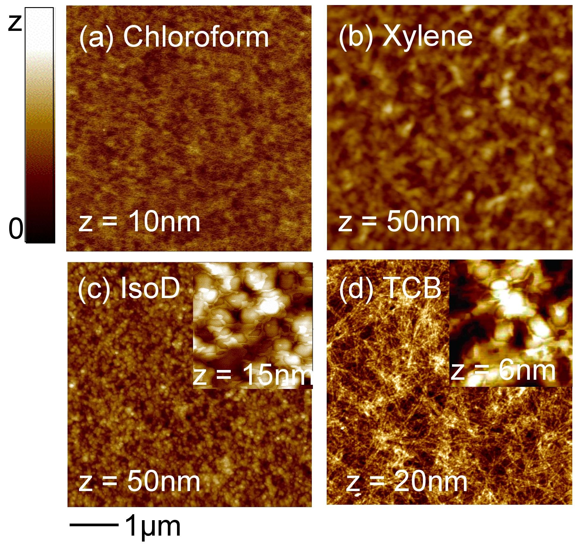
To verify that the changes in the spectra are microstructural in origin, we have studied the morphology of the films using AFM. Fig. 2 shows AFM images of films spun from various solvents. The films spun from high bp solvents show rough surfaces (isodurene film root-mean-square (rms) roughness 5.7 nm), while those spun from low bp solvents are smoother (chloroform film rms roughness 0.95 nm). The roughness is due to the formation of micro-structures Chang et al. (2000); Kline and McGehee (2006); Chang et al. (2004); Berson et al. (2007); Moule et al. (2008).
We therefore find that films with increased average conjugation lengths, order and percentage of crystalline structures, as predicted from the absorption spectra, demonstrate morphologies with micro-crystalline structures. Those with an increased percentage of disordered regions in the film demonstrate amorphous films. The absorption spectrum is therefore a useful and easy-to-measure tool to determine film micro-structure.
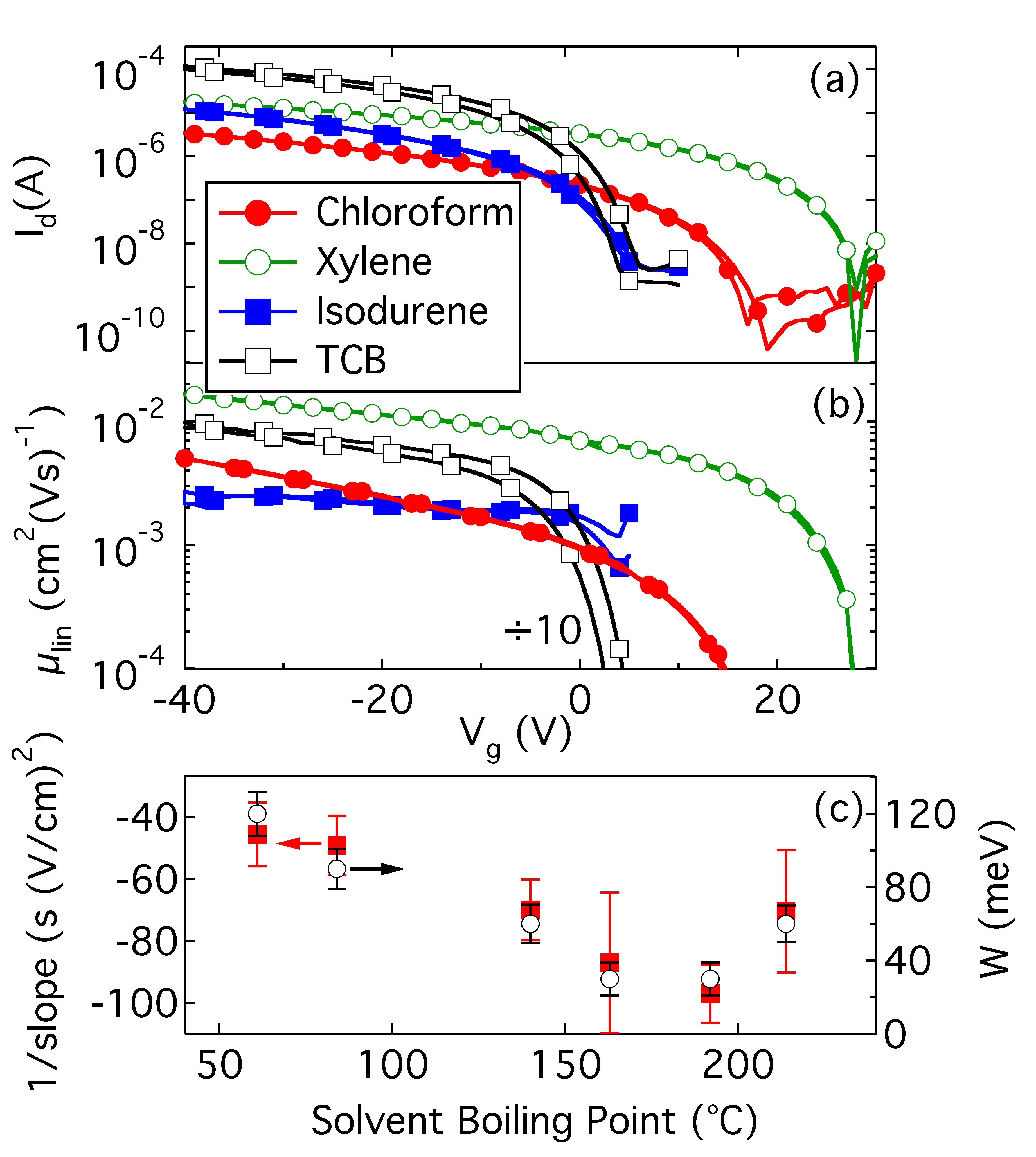
Transfer curves and plots of mobility versus gate-voltage (Vg) of transistors spun from a variety of solvents are shown in Fig.s 3 (a) and (b), respectively. Using a linear fit of the forward sweep of the mobility, from Vg=-10 to -40 V, we estimated how the slope of the mobility versus Vg changes as a function of solvent bp. This is shown in Fig. 3 (c) (left axis). Also plotted is the free exciton bandwidth, (right axis), reproduced from Fig. 1 (c). There is an excellent correlation between , obtained from the absorbance spectra, and the degree to which the mobility is Vg-dependent. Changes in slope of the mobility versus Vg as a function of solvent bp have previously been noted Chang et al. (2004) and have been explained in the context of the multiple trapping and release model Horowitz et al. (1999); Sirringhaus et al. (1998); Salleo et al. (2004); Sirringhaus (2005). The model assumes a large concentration of localized states below the mobility edge. At low Vg, most of the charges fill the localized states (traps) and the mobility is low. As Vg increases more of the traps are filled as the Fermi level moves closer to the mobility edge. More charges can be released to the extended, mobile states which leads to an increase in the effective mobility. At sufficiently high Vg, all of the traps are filled and any additional charges are injected into the extended states. Once this occurs, the mobility is constant with Vg. The degree to which the mobility is a function of Vg is thus dependent on the width of the localized density of states below the mobility edge. Shallow trap distributions will result in a weakly Vg-dependent mobility, while wider trap distributions will result in a pronounced Vg-dependence. From Fig. 3 we can therefore deduce that, for example, the device spun from isodurene has a shallow distribution of traps, while that spun from chloroform has a wide trap distribution. There is a clear correlation between the crystalline quality, as determined from the absorbance spectrum, and the width of the trap distribution.
We note however, that if we assume that there is no change in spatial disorder between hopping sites, we would expect devices with wider trap distributions to have correspondingly lower mobilities. Fig. 3 (b) shows that this is not the case. The reason for this is unclear from our absorption spectra analysis, probably due to the fact that the absorbance spectra provides a measure of the bulk film microstructure, while properties at interfaces are often important, especially in FETs where transport occurs in a narrow region close to the dielectric/semiconductor interface Chang et al. (2006); Kline et al. (2006).
Nevertheless, we have demonstrated that the absorbance spectrum by itself, can be used as a simple yet powerful probe of thin film excitonic coupling, intrachain order and fraction of crystalline regions within the film. Furthermore, it can be used to predict the relative distribution of trap states below the mobility edge in FETs, providing evidence that the quality of the crystallites is homogeneous throughout the film and does not change between the bulk and the interface. Therefore, linear absorption spectroscopy is a usefully simple tool to determine bulk film microstructure and this knowledge will help understanding of device characteristics in a variety of optoelectronic devices Moule et al. (2008).
Acknowledgements.
JC acknowledges support from EPSRC and an industrial Case award from Seiko Epson UK. CS acknowledges support from the NSERC and the Canada Research Chairs program. FCS is supported by the NSF, Grant No. DMR 0606028.References
- Sirringhaus et al. (1999) H. Sirringhaus, P. J. Brown, R. H. Friend, M. M. Nielsen, K. Bechgaard, B. M. W. Langeveld-Voss, A. J. H. Spiering, R. A. J. Janssen, E. W. Meijer, P. Herwig, D. M. de Leeuw, Nature 401, 685 (1999).
- McCullough et al. (1993) R. D. McCullough, S. Tristramnagle, S. P. Williams, R. D. Lowe, and M. Jayaraman, J. Am. Chem. Soc. 115, 4910 (1993).
- Kline and McGehee (2006) R. J. Kline and M. D. McGehee, Polymer Rev. 46, 27 (2006).
- Spano (2005) F. C. Spano, J. Chem. Phys. 122, 234701 (2005).
- Spano (2006) F. C. Spano, Chem. Phys. 325, 22-35 (2006).
- Clark et al. (2007) J. Clark C. Silva, R. H. Friend, and F. C. Spano, Phys. Rev. Lett. 98, 206406 (2007).
- Moule et al. (2008) A. J. Moulé and K. Meerholz, Adv. Mater. 20, 240 (2008).
- Berson et al. (2007) S. Berson R. De Bettingnies, S. Bailly, and S. Guillerez, Adv. Func. Mater. 17, 1377 (2007).
- Louarn et al. (1996) G. Louarn, M. Trznadel, J. P. Buisson, J. Laska, A. Pron, M. Lapkowski, and S. Lefrant, J. Phys. Chem. 100, 12532 (1996).
- Manas and Spano (1998) E. S. Manas and F. C. Spano, J. Chem. Phys. 109, 8087 (1998).
- Beljonne et al. (2000) D. Beljonne, J. Cornil, R. Silbey, P. Millie, and J. L. Bredas, J. Chem. Phys. 112, 4749 (2000).
- Barford (2000) W. Barford, J. Chem. Phys. 126, 134905 (2007).
- Chang et al. (2000) R. Chang, J. H. Hsu, W. S. Fann, J. Yu, S. H. Lin, Y. Z. Lee, and S. A. Chen, Chem. Phys. Lett. 317, 153 (2000).
- Chang et al. (2004) J. F. Chang, B. Q. Sun, D. W. Breiby, M. M. Nielsen, T. I. Solling, M. Giles, I. McCulloch, and H. Sirringhaus, Chem. Mater. 16, 4772 (2004).
- Sirringhaus et al. (1998) H. Sirringhaus, N. Tessler, and R. H. Friend, Science 280, 1741 (1998).
- Sirringhaus (2005) H. Sirringhaus, Adv. Mater. 17, 2411 (2005).
- Salleo et al. (2004) A. Salleo, T. W. Chen, A. R. Volkel, Y. Wu, P. Liu, B. S. Ong, and R. A. Street, Phys. Rev. B 70 (2004).
- Horowitz et al. (1999) G. Horowitz, R. Hajlaoui, D. Fichou, and A. El Kassmi, J. Appl. Phys. 85, 3202 (1999).
- Kline et al. (2006) R. J. Kline, M. D. McGehee, and M. F. Toney, Nature Materials 5, 222 (2006).
- Chang et al. (2006) J. F. Chang, J. Clark, N. Zhao, H. Sirringhaus, D. W. Breiby, J. W. Andreasen, M. M. Nielsen, M. Giles, M. Heeney, and I. McCulloch, Phys. Rev. B 74, 115318 (2006).


