Electron transport through honeycomb lattice ribbons
with armchair edges
Santanu K. Maiti1,2,∗
1Theoretical Condensed Matter Physics Division,
Saha Institute of Nuclear Physics,
1/AF, Bidhannagar, Kolkata-700 064, India
2Department of Physics, Narasinha Dutt College,
129, Belilious Road, Howrah-711 101, India
Abstract
We address electron transport in honeycomb lattice ribbons with armchair edges attached to two semi-infinite one-dimensional metallic electrodes within the tight-binding framework. Here we present numerically the conductance-energy and current-voltage characteristics as functions of the length and width of the ribbons. Our theoretical results predict that for a ribbon with much smaller length and width, so-called a nanoribbon, a gap in the conductance spectrum appears across the energy . While, this gap decreases gradually with the increase of the size of the ribbon, and eventually it almost vanishes. This reveals a transformation from the semiconducting to the conducting material, and it becomes much more clearly visible from our presented current-voltage characteristics.
PACS No.: 73.63.-b; 73.63.Rt.
Keywords: Honeycomb lattice ribbon; Armchair edges; Conductance; - characteristic.
∗Corresponding Author: Santanu K. Maiti
Electronic mail: santanu.maiti@saha.ac.in
1 Introduction
The electronic transport in nanoribbons of graphene has opened up new areas in nanoelectronics. A graphene nanoribbon (GNR) is a monolayer of carbon atoms arranged in a honeycomb lattice structure [1, 2, 3, 4]. Due to the special electronic and physical properties, graphene based materials exhibit several novel properties like unconventional quantum Hall effect [5], high carrier mobility [3] and many others. The high carrier mobility in graphene demonstrates the idea for fabrication of high speed switching devices those have widespread applications in different fields. Some recent experiments [6, 7, 8] have also suggested that GNRs can be used to design field-effect transistors and this application provides a huge interest in the community of nanoelectronics device research. Furthermore, GNRs can be used to construct MOSFETs which perform much better than conventional Si MOSFETs. In other experiment [9] it has been proposed that a narrow strip of graphene with armchair edges, so-called a graphene nanoribbon, exhibits semiconducting behavior due to its edge effects, unlike carbon nanotubes of larger sizes which are mixtures of both metallic and semiconducting materials. This is due to the fact that in a narrow graphene sheet, a band gap appears across the energy , while the gap gradually disappears with the increase of the size of the ribbon. This reveals a transformation from the semiconducting to the metallic material, and such a phenomenon can be utilized for fabrication of electronic devices. This motivates us to study the electron transport in honeycomb lattice ribbons with armchair edges and to verify qualitatively how the transformation from the semiconducting to the conducting property can be achieved simply by tuning the size of a ribbon.
The purpose of the present paper is to provide a qualitative study of
electron transport in honeycomb lattice ribbons with armchair edges
attached to two semi-infinite one-dimensional metallic electrodes (see
Fig. 1). The theoretical description of electron transport
in a bridge system has been followed based on the pioneering work of Aviram
and Ratner [10]. Later, many excellent experiments [11, 12, 13, 14, 15] have been done in several bridge systems to
understand the basic mechanisms underlying the electron transport. Though
in literature many theoretical [16, 17, 18, 19, 20, 21, 22, 23, 24, 25, 26, 27, 28, 29, 30, 31, 32] as well as
experimental papers [11, 12, 13, 14, 15] on electron transport
are available, yet lot of controversies are still present between the theory
and experiment, and the complete knowledge of the conduction mechanism in
this scale is not very well established even today.
Several controlling parameters are there which can regulate significantly
the electron transport in a conducting bridge, and all these effects have
to be taken into account properly to reveal the transport properties. For our
illustrative purposes, here we describe very briefly some of these effects.
(i) The quantum interference effect [33, 34, 35, 36, 37]
of electron waves passing through different arms of any conducting element
which bridges two electrodes becomes the most significant issue.
(ii) The coupling of
the electrodes with bridging material provides an important signature in
the determination of current amplitude across any bridge system [33].
The understanding of this coupling to the electrodes under non-equilibrium
condition is a major challenge, and we should take care about it in
fabrication of any electronic device.
(iii) The geometry
of the conducting material between the two electrodes itself is an important
issue to control the electron transmission. To emphasize it, Ernzerhof
et al. [38] have predicted several model calculations and
provided some significant results.
(iv) The dynamical fluctuation in
the small-scale devices is another important factor which plays an active
role and can be manifested through the measurement of shot
noise [39, 40], a direct consequence of the quantization of
charge. It can be used to obtain information on a system which is not
available directly through the conductance measurements, and is generally
more sensitive to the effects of electron-electron correlations than the
average conductance.
Furthermore, several other parameters of the Hamiltonian that describe a system also provide significant effects in the determination of the current across a bridge system.
Here we adopt a simple tight-binding model to describe the system and all the calculations are performed numerically. We address the conductance-energy and current-voltage characteristics as functions of lengths and widths of ribbons. Our results clearly predicts how a honeycomb lattice ribbon with armchair edges transforms its behavior from the semiconducting to the metallic nature, and this feature may be utilized in fabrication of nanoelectronic devices.
The paper is organized as follow. Following the introduction (Section ), in Section , we present the model and the theoretical formulations for our calculations. Section discusses the significant results, and finally, we summarize our results in Section .
2 Model and the synopsis of the theoretical background
Let us refer to Fig. 1, where a honeycomb lattice ribbon with armchair edges is attached to two semi-infinite one-dimensional metallic electrodes, viz, source and drain. It is important to note that throughout

this study we attach the electrodes at the two extreme ends of nanoribbons, as seen in Fig. 1, to keep the uniformity of the quantum interference effects.
To calculate the conductance of the ribbon, we use the Landauer conductance formula [41, 42], and at very low temperature and bias voltage it can be expressed in the form,
| (1) |
where gives the transmission probability of an electron in the ribbon. This can be represented in terms of the Green’s function of the ribbon and its coupling to the two electrodes by the relation [41, 42],
| (2) |
where and are respectively the retarded and advanced Green’s functions of the ribbon including the effects of the electrodes. The parameters and describe the coupling of the ribbon to the source and drain respectively, and they can be defined in terms of their self-energies. For the full system i.e., the ribbon, source and drain, the Green’s function is defined as,
| (3) |
where . is the injecting energy of the source electron and gives an infinitesimal imaginary part to . To Evaluate this Green’s function, the inversion of an infinite matrix is needed since the full system consists of the finite ribbon and the two semi-infinite electrodes. However, the entire system can be partitioned into sub-matrices corresponding to the individual sub-systems and the Green’s function for the ribbon can be effectively written as,
| (4) |
where is the Hamiltonian of the ribbon which can be written in the tight-binding model within the non-interacting picture like,
| (5) |
In the above Hamiltonian (), ’s are the site energies, () is the creation (annihilation) operator of an electron at the site and is the nearest-neighbor hopping integral. Similar kind of tight-binding Hamiltonian is also used to describe the two semi-infinite one-dimensional perfect electrodes where the Hamiltonian is parametrized by constant on-site potential and nearest-neighbor hopping integral . In Eq. 4, and are the self-energy operators due to the two electrodes, where and correspond to the Green’s functions of the source and drain respectively. and are the coupling matrices and they will be non-zero only for the adjacent points of the ribbon, and the electrodes respectively. The matrices and can be calculated through the expression,
| (6) |
where and are the retarded and advanced self-energies respectively, and they are conjugate with each other. These self-energies can be written as [43],
| (7) |
where are the real parts of the self-energies which correspond to the shift of the energy eigenvalues of the ribbon and the imaginary parts of the self-energies represent the broadening of these energy levels. Since this broadening is much larger than the thermal broadening, we restrict our all calculations only at absolute zero temperature. All the informations about the ribbon-to-electrode coupling are included into these two self-energies.
The current passing across the ribbon can be depicted as a single-electron scattering process between the two reservoirs of charge carriers. The current can be computed as a function of the applied bias voltage through the relation [41],
| (8) |
where is the equilibrium Fermi energy. Here we make a realistic assumption that the entire voltage is dropped across the ribbon-electrode interfaces, and it is examined that under such an assumption the - characteristics do not change their qualitative features. This assumption is based on the fact that, the electric field inside the ribbon especially for narrow ribbons seems to have a minimal effect on the conductance-voltage characteristics. On the other hand, for quite larger ribbons and high bias voltages the electric field inside the ribbon may play a more significant role depending on the internal structure and size of the ribbon [43], but the effect becomes too small.
3 Results and discussion
In order to understand the dependence of electron transport on the lengths and widths of nanoribbons, in the present article, we concentrate only on the cleaned systems rather than any dirty one. Accordingly, we set the site energies of the honeycomb lattice ribbons as for all . The values of the other parameters are assigned as follow: the nearest-neighbor hopping integral in the ribbon is set to , the on-site energy and the hopping integral for the two electrodes are fixed to and respectively. The parameters and are set as , where they correspond to the hopping strengths of the ribbon to the source and drain respectively. In addition to these, we also introduce two other parameters and to reveal the size of a nanoribbon, where they correspond to the width and length of the ribbon respectively. Thus, for example, a nanoribbon with and represents a linear chain of four hexagons. Hence the parameter determines the total number of hexagons in a single chain. Following this rule, a nanoribbon with and corresponds to three linear chains attached side by side (see Fig. 1) where each chain contains three hexagons. For simplicity, throughout our study we set the Fermi energy and choose the units where .
Let us first describe the variation of the conductance as a function of the injecting electron energy . In Fig. 2 we present the conductance-energy (-) characteristics for some honeycomb lattice ribbons with fixed width () and varying lengths, where (a) and (b) correspond to the linear chains with six () and ten () hexagons
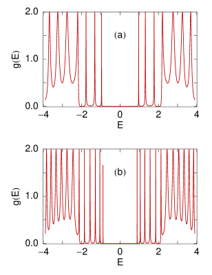
respectively. The conductance spectra shows fine resonance peaks for some particular energies, while for all other values of the energy , either it () drops to zero or gets much small value. At these resonance energies, the conductance gets the value , and hence, the transmission probability becomes unity since the expression holds from the Landauer conductance formula (see Eq. 1). These resonance peaks are associated with the energy levels of the nanoribbons and thus the conductance spectra, on the other hand, reveal the signature of the energy spectra of the nanoribbons. The most important issue observed from these spectra is that, a central gap appears across the energy and the width of the gap becomes small for the chain with hexagons compared to the other chain i.e., the chain with hexagons. It predicts that, for a fixed width, the central energy gap decreases with the increase of the length of the nanoribbon. In the same footing, to visualize the dependence of the width on the conductance-energy characteristics, in Fig. 3 we display the results for some honeycomb lattice ribbons
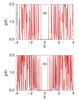
considering the width , where (a) and (b) represent the nanoribbons with identical lengths as in Fig. 2. The results show that, due to the large system sizes the - characteristics exhibit almost a quasi-continuous variation across the energy . For both these two ribbons the energy gap also appears around the energy , and the gap decreases with the increase of the length of the nanoribbon. Comparing the results presented in Figs. 2 and 3, we can emphasize that for a fixed width the central energy gap always decreases with the size of the nanoribbon. Now to reveal the dependence of the energy gap on the system size much more clearly, in Fig. 4 we show the variation of the central energy gap as a function of the length for some honeycomb lattice ribbons with different widths . The red, green and blue lines correspond to the results for the ribbons with fixed widths , and respectively. These results clearly emphasize that for the fixed width the gap gradually decreases with the increase of the length of the nanoribbon. It is also examined that for much larger lengths it () almost vanishes (not shown here in the figure). Quite similar nature is also observed if we plot the variation of the energy gap as a function of the length keeping the width as a constant, and due to the obvious reason we do not plot these
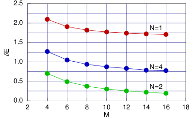
results further in the present description. These results provide us an important signature which concern with a transition from the semiconducting (finite energy gap) to the conducting (zero energy gap) material, and this transition can be achieved simply by tuning the size of the nanoribbon.
All these basic features of electron transfer can be quite easily explained from our study of the current-voltage (-) characteristics rather than the conductance-energy spectra. The current is determined from the integration procedure of the transmission function () (see Eq. 8), where the function varies exactly similar to the conductance spectra, differ only in magnitude by a factor , since the relation holds from the Landauer conductance formula (Eq. 1). The variation of the current-voltage characteristics for some typical honeycomb lattice ribbons with fixed width and varying lengths is presented in Fig. 5, where (a) and (b) correspond to the ribbons with and respectively. The current exhibits a staircase
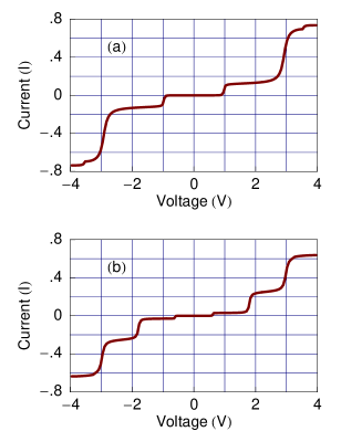
like behavior as a function of the applied bias voltage . This staircase like nature appears due to the existence of the resonance peaks in the conductance spectra since the current is computed by the integration process of the transmission function . As we increase the bias voltage , the electrochemical potentials in the two electrodes cross one of the energy levels of the ribbon and accordingly a jump in the - curve appears. The sharpness of the steps in the current-voltage characteristics and the current amplitude solely depend on the coupling strengths of the nanoribbon to the electrodes, viz, source and drain. It is observed that, in the limit of weak coupling, defined by the condition , current shows staircase like structure with sharp steps. While, in the strong coupling limit, described by the condition , current varies quite continuously with the bias voltage and achieves large current amplitude compared to the weak-coupling limit. All these coupling effects have clearly been explained in many papers in the literature. The significant feature observed from the figure (Fig. 5) is that for the
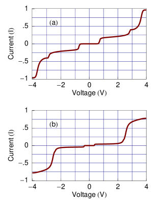
fixed width (), the threshold bias voltage () of electron conduction decreases with the increase of the length of the ribbon. This reveals a transformation towards the conducting material. Quite in the same fashion, to see the variation of the threshold bias voltage for other system sizes, in Fig. 6 we plot the results for some nanoribbons with fixed width and varying lengths where (a) and (b) correspond to the ribbons with and respectively. The results show that the threshold bias voltages decrease much more compared to the nanoribbons of width . Thus both from Figs. 5 and 6 we clearly observe that can be regulated very nicely by tuning the size (both length and width) of the nanoribbon. For quite larger ribbons the threshold bias voltage eventually reduces to zero. This clearly manifests the transformation from the semiconducting to the conducting material.
4 Concluding remarks
To summarize, we have addressed electron transport in honeycomb lattice ribbons with armchair edges attached to two semi-infinite one-dimensional metallic electrodes within the tight-binding framework. Our results have predicted that for ribbons with smaller lengths and widths, a central gap in the conductance spectrum appears across the energy . While, this gap decreases gradually as we increase the size of the ribbon and eventually it almost vanishes. This reveals a transformation from the semiconducting to the conducting behavior, and it has been much more clearly described from the presented current-voltage characteristics which provide that the threshold bias voltage of electron conduction decreases gradually with the increase of the size of the ribbon.
This is our first step to describe how the electron transport in honeycomb lattice ribbons with armchair edges depends on the length and width of the ribbons. Here we have made several realistic assumptions by ignoring the effects of the electron-electron correlation, disorder, temperature, etc. All these effects can be incorporated quite easily with this present formalism and we need further study in such systems. In our next work we are investigating the electron transport properties in honeycomb lattice ribbons with zigzag edges.
References
- [1] V. V. Cheianov, V. Fal’ko and B. L. Altshuler, Science 315, 1252 (2007).
- [2] J. B. Pendry, Science 315, 1226 (2007).
- [3] A. K. Geim and K. S. Novoselov, Nat. Mater. 6, 183 (2007).
- [4] C. Berger, Z. Song, X. Li, X. Wu, N. Brown, C. Naud, D. Mayou, T. Li, J. Hass, A. N. Marchenkov, E. H. Corrad, P. N. First and W. A. de Heer, Science 312, 1191 (2006).
- [5] Y. Zhang, Y. Tan, H. L. Stormer and P. Kim, Nature 438, 201 (2005).
- [6] Y. Ouyang, Y. Yoon, J. K. Fodor and J. Guo, Appl. Phys. Lett. 89, 203107 (2006).
- [7] Q. Yan, B. Huang, J. Yu, F. Zheng, J. Zang, J. Wu, B.-L. Gu, F. Liu and W. Duan, Nano Lett. 7, 1469 (2007).
- [8] D. A. Areshkin and C. T. White, Nano Lett. 7, 3253 (2007).
- [9] X. Li, X. Wang, L. Zhang, S. Lee, H. Dai, Science 319, 1229 (2008).
- [10] A. Aviram and M. Ratner, Chem. Phys. Lett. 29, 277 (1974).
- [11] T. Dadosh, Y. Gordin, R. Krahne, I. Khivrich, D. Mahalu, V. Frydman, J. Sperling, A. Yacoby and I. Bar-Joseph, Nature 436, 677 (2005).
- [12] J. Chen, M. A. Reed, A. M. Rawlett and J. M. Tour, Science 286, 1550 (1999).
- [13] M. A. Reed, C. Zhou, C. J. Muller, T. P. Burgin and J. M. Tour, Science 278, 252 (1997).
- [14] K. S. Novoselov, A. K. Geim, S. V. Morozov, D. Jiang, M. I. Kastnelson, I. V. Grigorieva, S. V. Dubonos and A. A. Firsov, Nature (London) 438, 197 (2005).
- [15] K. S. Novoselov, A. K. Geim, S. M. Morozov, D. Jiang, Y. Zhang, S. V. Dubonos, I. V. Grigorieva and A. A. Firsov, Science 306, 666 (2004).
- [16] K. Wakabayashi, Phys. Rev. B 64, 125428 (2001).
- [17] K. Wakabayashi, M. Fujita, H. Ajiki and M. Sigrist, Phys. Rev. B 59, 8271 (1999).
- [18] K. Wakabayashi, J. Phys. Chem. Solid. 69, 1162 (2008).
- [19] K. Wakabayashi and M. Sigrist, Synth. Metal. 121, 1231 (2001).
- [20] G. Liang, N. Neophytou, M. S. Lundstrom and D. E. Nikonov, Nano Lett. 8, 1819 (2008).
- [21] O. Hod, J. E. Peralta and G. E. Scuseria, Phys. Rev. B 76, 233401 (2007).
- [22] A. Cresti, G. Grosso and G. P. Parravicini, Phys. Rev. B 76, 205433 (2007).
- [23] E. Cuansing and J. S. Wang, arXiv:0810.2181.
- [24] S. M. Cronenwett, T. H. Oosterkamp and L. P. Kouwenhoven, Science 281, 5 (1998).
- [25] A. W. Holleitner, R. H. Blick, A. K. Huttel, K. Eber and J. P. Kotthaus, Science 297, 70 (2002).
- [26] P. A. Orellana, M. L. Ladron de Guevara, M. Pacheco and A. Latge, Phys. Rev. B 68, 195321 (2003).
- [27] P. A. Orellana, F. Dominguez-Adame, I. Gomez and M. L. Ladron de Guevara, Phys. Rev. B 67, 085321 (2003).
- [28] A. Nitzan, Annu. Rev. Phys. Chem. 52, 681 (2001).
- [29] A. Nitzan and M. A. Ratner, Science 300, 1384 (2003).
- [30] D. M. Newns, Phys. Rev. 178, 1123 (1969).
- [31] V. Mujica, M. Kemp and M. A. Ratner, J. Chem. Phys. 101, 6849 (1994).
- [32] V. Mujica, M. Kemp, A. E. Roitberg and M. A. Ratner, J. Chem. Phys. 104, 7296 (1996).
- [33] R. Baer and D. Neuhauser, Chem. Phys. 281, 353 (2002).
- [34] R. Baer and D. Neuhauser, J. Am. Chem. Soc. 124, 4200 (2002).
- [35] D. Walter, D. Neuhauser and R. Baer, Chem. Phys. 299, 139 (2004).
- [36] K. Tagami, L. Wang and M. Tsukada, Nano Lett. 4, 209 (2004).
- [37] K. Walczak, Cent. Eur. J. Chem. 2, 524 (2004).
- [38] M. Ernzerhof, M. Zhuang and P. Rocheleau, J. Chem. Phys. 123, 134704 (2005).
- [39] Y. M. Blanter and M. Buttiker, Phys. Rep. 336, 1 (2000).
- [40] K. Walczak, Phys. Stat. Sol. (b) 241, 2555 (2004).
- [41] S. Datta, Electronic transport in mesoscopic systems, Cambridge University Press, Cambridge (1997).
- [42] M. B. Nardelli, Phys. Rev. B 60, 7828 (1999).
- [43] W. Tian, S. Datta, S. Hong, R. Reifenberger, J. I. Henderson and C. I. Kubiak, J. Chem. Phys. 109, 2874 (1998).