Heat conductance is strongly anisotropic for pristine silicon nanowires
Abstract
We compute atomistically the heat conductance for ultra-thin pristine silicon nanowires (SiNWs) with diameters ranging from 1 to 5 nm. The room temperature thermal conductance is found to be highly anisotropic: wires oriented along the direction have 50–75% larger conductance than wires oriented along the and directions. We show that the anisotropies can be qualitatively understood and reproduced from the bulk phonon band structure. Ab initio density functional theory (DFT) is used to study the thinnest wires, but becomes computationally prohibitive for larger diameters, where we instead use the Tersoff empirical potential model (TEP). For the smallest wires, the thermal conductances obtained from DFT- and TEP calculations agree within 10%. The presented results could be relevant for future phonon-engineering of nanowire devices.
Thermal transport properties of silicon nanowires (SiNWs) are crucial for many of their future applications. A high thermal conductance of SiNWs is desirable in nano-electronic components, while, on the other hand, a low thermal conductance is beneficial for thermoelectric applications. Indeed, recent experiments have demonstrated that SiNWs can have a significantly higher thermoelectric performance than bulk silicon [1, 2], due to a reduced thermal conductance of the nanowires [3]. Raman microscopy studies have revealed significant phonon confinement effects in SiNWs down to 4 nm in diameter[4]. Very thin SiNWs with diameters below 5 nm have been synthesized by several groups [4, 5, 6, 7] typically oriented in the , , , or directions.
Most theoretical works on phonon transport in nanowires have been based on continuous elasticity theory and the Boltzmann transport equation, e.g. [8, 9]. Recently, however, some theoretical work based on atomistic models has been reported: Mingo et al. obtained good agreement with experiments for wires with diameters nm [10, 11]; Wang et al. [12] studied the diameter dependence of pristine wires, and Zhang et al. [13] analyzed the interface scattering between nanowires and bulk contacts. The effects of an amorphous coating on the transmission was studied in Ref. [14].
An important design parameter for SiNW devices is the crystal orientation of the wires, and it is thus highly relevant to compare the thermal transport in the different wire directions. Several recent works have already addressed the directional dependence on the electronic transport properties [15, 16, 17, 18, 19]. To our knowledge, no experimental comparison of heat conduction in different wire orientations in SiNWs has been published. In wires connected to bulk contacts, Zhang et al. [13] found only insignificant difference between and wires. Early measurements [20, 21] of anisotropic heat conduction and phonon focusing in bulk silicon was analyzed theoretically [22] for boundary-scattered phonons in macroscopic samples. However, in very narrow SiNWs with smooth surfaces there will be no surface scattering, since the surface structure is incorporated in the phonon modes. In the ideal ballistic limit, all phonon modes will propagate through the wire with a transmission probability of one.
In this work we compute the thermal conductance of ultra thin silicon nanowires (SiNWs) with diameters from 1–5 nm oriented along the , , and directions. As a first step we use both DFT calculations [23] and empirical potentials [24, 25] to calculate the dynamical matrix. Next, the Landauer transmission and thermal conductance are calculated. We find that the room temperature thermal transport is highly anisotropic with wires having up to two times larger thermal conductance than and . Finally, we show that the anisotropies can be understood based on the underlying bulk phonon band structure.
We use atomic orbital DFT calculations [23] to study the smallest wires (diameter nm) in the and directions. After an initial relaxation, each atom, , is displaced by in direction to obtain the forces, , on atom in direction [31]. The dynamical matrix, , is then found by finite differences [32]
| (1) |
with being the total energy. The intra-atomic elements are calculated by imposing momentum conservation, such that . The forces are relatively long ranged and we found it necessary to use periodically repeated super cells containing at least 5 unit cells, corresponding to a minimum length Å in the direction. This implies that the calculations become very time consuming and puts strong limitations on the diameter range to be investigated.
Since the large-diameter DFT calculations become computationally prohibitive, one needs a faster computational scheme. To this end we use the Tersoff empirical potential model (TEP) [24, 33] as implemented in the ”General Lattice Utility Program” (gulp)[25]. We use gulp to relax the atomic structure and to directly output the dynamical matrix, , for the relaxed system. The interactions in the TEP are highly local, and the calculations can be carried out on periodically repeated super cells containing only two unit cells. The TEP calculations are much faster ( times) and much less memory demanding than the DFT calculations. In order to validate the empirical scheme, we present below comparisons between the DFT and TEP schemes.
Experimentally fabricated SiNWs are typically passivated with either amorphous silicon oxide, SiO2, [7] or with hydrogen [5]. The influence of amorphous SiO2 passivation on phonon transport was investigated by Mingo and Yang [14]. However, atomistic models of amorphous SiO2 are demanding and often one uses hydrogen in calculations of the electronic transport to passivate the silicon dangling bonds [26, 27, 28]. The surface passivation is crucial for the electronic properties since the Si dangling bonds form states in the bandgap possibly leading to metallic SiNWs [29]. Passivation by hydrogen suppresses surface reconstruction and leads to semiconducting wires. We thus include hydrogen when we model SiNWs using DFT calculations. We show below, that it is not necessary to include H-passivation in the TEP model.
We formally divide our system into a left, central, and right region. The left and right contacts are modeled as two semi-infinite pristine wires. In the present study, the central region is also a pristine wire, but it could in principle include any structural defects [14, 34, 35] as we shall describe in a forthcoming paper [36]. In the limit of a small temperature difference between the left and right regions, the thermal conductance is [34, 37, 38]
| (2) |
is the transmission function, which in the ideal ballistic limit equals the number of phonon subbands, , at frequency (see Fig. 2). In the low temperature limit we can approximate , since there are four acoustic modes at [39]. The remaining integral in Eq.(2) can be calculated analytically to yield the universal thermal conductance quantum .
Figure 1 shows the thermal conductance, , vs. temperature for a 1.2 nm diameter wire and a 1.0 nm diameter wire.
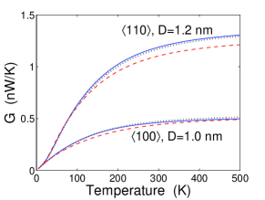
The results obtained with the TEP model agree quite well with the microscopic DFT calculations. At temperatures K, the relative error is less than 5%, and at K the difference is within 10%. Also, observe that including hydrogen in the empirical potential calculations leads to a maximum deviation of 3% (at K, wire) as compared to the pure Si calculations. Leaving out the hydrogen in the TEP calculations is therefore justified. We take these results as a validation of the relatively simple and fast empirical potential calculations on pure Si wires, and proceed to study much larger wires - a study that would be very time consuming using DFT calculations. In the rest of this paper, we study the diameter dependence of , and oriented SiNWs (see Figure 2), using the TEP approach without H-passivation. We note that the same approximation was recently applied in Refs. [12, 30].
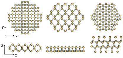
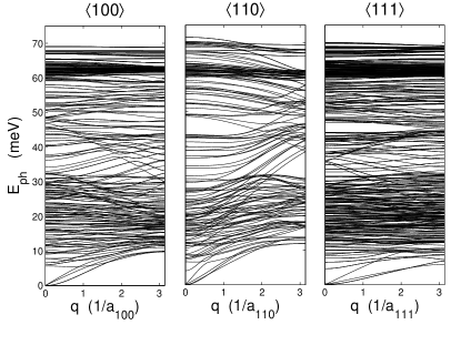
Figure 2 shows the atomic structure in the periodically repeated unit cell (along the -axis) of 2 nm diameter wires with the three orientations. The top row shows a cross section of the wires while in the middle row we have shown side views of the unit cells. In the bottom panel the full phonon band structures for the three wires are shown. For each wire there are subbands, with being the number of atoms in the unit cell. Note that the different wire orientations have different unit cell lengths, , and thus also different number of atoms in the unit cell. At low energies there are only four acoustic modes: the dilatational and the torsional modes with linear dispersions and two flexural modes with quadratic dispersions [39]. The many, relatively flat subbands starting right above the acoustic modes are denoted shear modes and originate from the bulk acoustic bands that are folded into the wire axis. The many closely lying bands around meV correspond to the bulk LO phonon energy.
An important qualitative feature is that the bands in the wire generally have a larger slope (velocity) than the the other wire orientations, where there are many flat bands. The same trend is also seen for other wire diameters. Due to the larger slope there are more bands at a given energy for the wires, and one expects , leading to a larger thermal conductance for the wire.
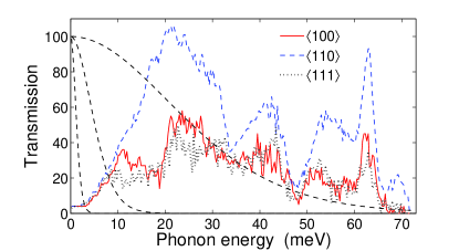
This anisotropy is further illustrated in Fig. 3 showing the transmission function for three different wires orientations, all having diameter nm. While the and wires have approximately the same transmission, the wire has a significantly larger transmission at most energies above 10 meV. The three black dashed curves show the function appearing in eq 2 at temperatures K. We observe that at K, all wires have , and display the quantized thermal conductance, .
The curve K) suggests that the thermal conductance of the three wires should be approximately the same up to temperatures K. At higher temperatures, the wires will have a higher conductance.
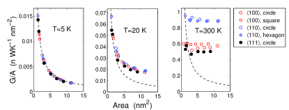
Figure 4 shows the thermal conductance per unit area, , vs. cross sectional area, , at different temperatures [40]. The different symbols correspond to different wire orientations and different cross sectional shapes of the wires. At low temperatures (5 K, left) all wires have the same dependence and coincide with the analytical result shown as the dashed line in the graphs. At K (middle), the area dependence of the three wires is still approximately the same as expected from Fig. 3. Note that the thinnest wires still follow the quantum line, . This is because confinement lifts the bottom of the shear modes (see Fig. 2) and increases the energy range, where only the four acoustic modes exist.
At K (right) is almost area independent. The room temperature area normalized conductances of the oriented wires are approximately 50% and 75% larger than the and wires, respectively. The small fluctuations in for a given orientation are due to variations in the surface structure of the wires at different diameters. Notice also that for the orientation, the square shaped wires have a larger conductance than the circular shaped wires. Again, we attribute this to the details in the surface structure. The room temperature conductance per unit area of the and wires are in fairly good agreement with values reported in Ref. [12] and [13], respectively.
Experimental [3] and theoretical [10] works have shown that the thermal conductivity decreases with decreasing diameter, seemingly contradicting the results shown in Fig. 4. However, we have not included any scattering (surface roughnes, impurity, phonon-phonon, phonon-electron) in our calculations, and our results thus represents an ideal upper limit for the thermal conductance. Indeed, if we include scattering by vacancies we observe a decreasing conductance per unit area with decreasing diameter [36]. Quantitative comparison with experiments should only be carried out in the fully ballistic regime for short wires at relatively low temperatures where anharmonic effects are unimportant, and for wires with very smooth surfaces.
The anisotropies can also be obtained from the bulk band structure. We construct an approximate wire band structure by projecting the bulk subband surfaces onto lines, , along the , , and directions. Figure 5 (top) shows the orientation of the basic tetrahedrals together with the direction of the lines. The lines are equidistantly spaced on a fine square grid in the plane perpendicular to the wire direction, and are restricted to the first Brillouin zone. A total number of lines gives projected subbands, since there are two atoms in the bulk primitive unit cell, and three bands per atom. From the projected band structure we obtain the transmission by counting the number of bands at a given energy. Each of the lines ranges from , with being the unit cell length of a wire in the direction. For a given cross sectional area, , the different wire orientations will have different numbers of atoms in the unit cell and thus also different number of bands (see Figure 2). To account for that, we scale the transmissions by a factor , where is the number of atoms in a wire unit cell, and Å-3 is the atomic density.

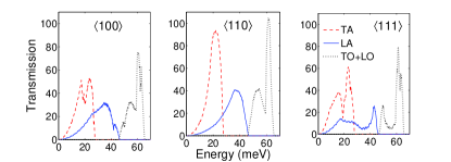
Figure 5 (bottom panel) shows the transmission functions obtained from the bulk band structure. The large peak in transmission around meV for the wire seen in Fig. 3 is reproduced from the bulk bands with the actual transmission values being in close agreement. The room temperature thermal conductances per unit area, , obtained from Fig. 5 are , , and nW/(K nm2), in qualitative agreement with the values in Fig. 4. Note, however, at low temperature the results are wrong, since the true wires have four acoustic modes, while the projected bulk band structures only have three. At higher temperatures, this error is less important.
Evidently, it is primarily the two TA subbands that are responsible for the large anisotropy. This is not surprising since the bulk band structure in the direction has two non-degenerate TA subbands while in the and directions the TA subbands are degenerate. Thus, importantly, the anisotropy is not merely a property of the specific silicon nanowires studied here, but can also be expected to take place in other materials with the diamond structure. Indeed, projection of the germanium bulk band structure as described above yields similar results.
In conclusion, we have shown that the ballistic thermal conductance in silicon nanowires is strongly anisotropic with wires oriented along the direction having 50% and 75% larger conductance per unit area than wires oriented along the and directions, respectively. We believe that the presented results will be relevant for future phonon-engineering of nanowire devices.
Acknowledgement. We thank the Danish Center for Scientific Computing (DCSC) and Direktør Henriksens Fond for providing computer resources. TM acknowledge the Denmark-America foundation for financial support. APJ is grateful to the FiDiPro program of the Finnish Academy.
References
- [1] Hochbaum, A.; Chen, R.; Delgado, R.; Liang, W.; Garnett, E.; Najarian, M.; Marumdar, A.; Yang, P. Nature 2008, 451, 163.
- [2] Boukai, A.; Bunimovich, Y.; Tahir-Kheli, J.; Yu, J.-K.; III, W. G.; Heath, J. Nature 2008, 451, 168.
- [3] Li, D.; Wu, Y.; Kim, P.; Shi, L.; Yand, P.; Majumdar, A. Appl. Phys. Lett. 2003, 83, 2934.
- [4] Adu, K.; Gutierrez, H.; Kim, U.; Sumanasekera, G.; Eklund, P. Nano Lett. 2005, 5, 409.
- [5] Ma, D. D. D.; Lee, C. S.; Au, F. K.; Tong, S. T.; Lee, S. T. Science 2003, 299, 1874.
- [6] Holmes, J. D.; Johnston, K.; Doty, R. C.; Korgel, B. A. Science 2000, 287, 1471-1473.
- [7] Wu, Y.; Cui, Y.; Huynh, L.; Barrelet, C.; Bell, D.; Lieber, C. Nano Lett. 2004, 4, 433-436.
- [8] Zou, J.; Balandin, A. J. Appl. Phys. 2001, 89, 2932.
- [9] Santamore, D.; Cross, M. Phys. Rev. Lett. 2001, 97, 115502.
- [10] Mingo, N. Phys. Rev. B 2003, 68, 113308.
- [11] Mingo, N.; Yang, L.; Li, D.; Majumdar, A. Nano Lett. 2003, 3, 1713.
- [12] Wang, J.; Wang, J.-S. Appl. Phys. Lett. 2007, 90, 241908.
- [13] Zhang, W.; Mingo, N.; Fisher, T. S. Phys. Rev. B 2007, 76, 195429.
- [14] Mingo, N.; Yang, L. Phys. Rev. B 2003, 68, 245406.
- [15] Zhao, X.; Wei, C. M.; Yang, L.; Chou, M. Phys. Rev. Lett. 2004, 92, 236805.
- [16] Niquet, Y. M.; Lherbier, A.; Quang, N. H.; Fernández-Serra, M. V.; Blase, X.; Delerue, C. Phys. Rev. B 2005, 73, 165319.
- [17] Rurali, R.; Aradi, B.; Frauenheim, T.; Gali, A. Phys. Rev. B 2007, 76, 113303.
- [18] Vo, T.; Williamson, J.; Galli, G. Phys. Rev. B 2006, 74, 045116.
- [19] Svizhenko, A.; Leu, P.; Cho, K. Phys. Rev. B 2007, 76, 125417.
- [20] Hurst, W. S.; Frankl, D. R. Phys. Rev. 1969, 186, 801–810.
- [21] McCurdy, A. K.; Maris, H. J.; Elbaum, C. Phys. Rev. B 1970, 2, 4077–4083.
- [22] McCurdy, A. Phys. Rev. B 1982, 26, 6971.
- [23] Soler, J. M.; Artacho, E.; Gale, J. D.; Garc a, A.; Junquera, J.; Ordejón, P.; Sánchez-Portal, D. J. Phys.: Condens. Matter 2002, 14, 2745-2779.
- [24] Tersoff, J. Phys. Rev. B 1988, 38, 9902.
- [25] Gale, J. JCS Faraday Trans. 1997, 93, 629.
- [26] Fernández-Serra, M.-V.; Adessi, C.; Blase, X. Nano Lett. 2006, 6, 2674-2678.
- [27] Fernández-Serra, M.; Adessi, C.; Blase, X. Phys. Rev. Lett. 2006, 96, 166805.
- [28] Markussen, T.; Rurali, R.; Jauho, A.-P.; Brandbyge, M. Phys. Rev. Lett. 2007, 99, 076803.
- [29] Rurali, R.; Lorente, N. Phys. Rev. Lett. 2005, 94, 026805.
- [30] Pascual-Gutierrez, J. A.; Murthy, J. Y.; Viskanta, R. J. Appl. Phys. 2007, 102, 034315.
- [31] We use a double zeta polarized basis set with an energy cutoff of 100 Ry. The structure is initially relaxed with a maximum residual force of 0.02 eV/Å. The ions are displaces by Å.
- [32] Frederiksen, T.; Paulsson, M.; Brandbyge, M.; Jauho, A.-P. Phys. Rev. B 2007, 75, 205413.
- [33] Tersoff, J. Phys. Rev. B 1989, 39, 5566.
- [34] Yamamoto, T.; Watanabe, K. Phys. Rev. Lett. 2006, 96, 25503.
- [35] Mingo, N.; Stewart, D.; Broido, D.; Srivastava, D. Phys. Rev. B 2008, 77, 033418.
- [36] Markussen, T.; Jauho, A.-P.; Brandbyge, M. in preparation.
- [37] Wang, J.-S.; Zeng, N.; Wang, J.; Gan, C.-K. Phys. Rev. E 2007, 75, 061128.
- [38] Mingo, N. Phys. Rev. B 2006, 74, 125402.
- [39] Cleland, A. Foundations of Nanomechanics; Springer: 2003.
- [40] We define the cross sectional area as , where is the number of atoms in a unit cell, Å-3 is the bulk atomic density, and is the unit cell length.