Two-Channel Kondo Effects in Al/AlOx/Sc Planar Tunnel Junctions
Abstract
We have measured the differential conductances in several Al/AlOx/Sc planar tunnel junctions between 2 and 35 K. As the temperature decreases to 16 K, the zero-bias conductance crosses over from a standard ln dependence to a novel dependence. Correspondingly, the finite bias conductance reveals a two-channel Kondo scaling behavior between 4 and 16 K. The observed two-channel Kondo physics is ascribed to originating from a few localized spin- Sc atoms situated slightly inside the AlOx/Sc interface.
pacs:
72.15.Qm, 64.70.Tg, 72.10.Fk, 73.40.RwHow conduction electrons interact with local degeneracies, which is the central theme of the Kondo effect Hewson , is a long-standing issue in many-body physics. In the original Kondo effect, the local degeneracies are provided by a spin- impurity, antiferromagnetically coupled to a single reservoir of free electrons [the single-channel Kondo (1CK) effect]. Well below a characteristic energy, the Kondo temperature , the localized moment is fully screened by the surrounding itinerant electrons to form a singlet ground state, leading to a standard Fermi liquid behavior Hewson . However, Nozières and Blandin Noz-MCK proposed that, in the multi-channel case, i.e., the screening channels , where is the spin of the localized moment, a non-Fermi liquid behavior may occur at low temperatures. The simplest version of the multi-channel Kondo phenomena is the two-channel Kondo (2CK) effect () which has recently attracted much theoretical Zawadowski1998 ; Andraka1994-Kim1995 ; Ott1983-Cox1987-Seaman1991 ; Zawadowski1980-Muramatsu1986 and experimental Ralph1994 ; Potok2007 ; Oreg2003 ; Cichorek2005 attention. Apart from a physical spin, the local degeneracies may arise from orbital quadrupolar degrees of freedom or nearby atomic positions, i.e., two-level systems (TLS) Zawadowski1998 . The magnetic and quadrupolar models have been utilized to explain the specific heat anomalies in certain heavy fermion compounds Zawadowski1998 ; Andraka1994-Kim1995 ; Ott1983-Cox1987-Seaman1991 , while the TLS-induced 2CK physics Zawadowski1998 ; Zawadowski1980-Muramatsu1986 has recently been experimentally realized in nanoscale metal point contacts Ralph1994 . Very lately, an artificial spin- semiconductor quantum dot coupled to two independent electron reservoirs has been elegantly constructed Potok2007 to test the 2CK physics Oreg2003 . Besides, the 2CK effect on electrical resistivity due to TLS is argued to be found in a ThAsSe single crystal Cichorek2005 . Thus far, there has been no observation of the 2CK effect caused by the “simple” 3 magnetic transition-metal atoms. In this work, we report our finding of a non-Fermi liquid behavior in Al/AlOx/Sc planar tunnel junctions where a number of spin- Sc atoms are present at or slightly inside the AlOx/Sc interface Wyatt1974 ; Appelbaum1967 .
Our planar tunnel junctions are composed of three layers: an Al (25 nm) film and a Sc (60 nm) film, separated by an insulating AlOx (1.5–2 nm) barrier. Both the Al and Sc films were thermally evaporated, while the AlOx layer was grown on the top surface of the Al film by oxygen glow discharge Yeh-thesis . The low-temperature resistivities of our Al (Sc) films were typically (4 K) 13 (70) cm. Lock-in techniques together with a bias circuitry were employed to measure the differential conductance as a function of both bias voltage and temperature. The modulation voltages used were smaller than so that the main smearing was due to the thermal energy. The quality of the insulating barriers was checked according to the Rowell criteria Rowell as well as by measuring the curves below the superconducting transition temperature ( 2 K) of the Al films. At 0.25 K, a deep superconducting gap was evidenced in all junctions, ensuring that the conduction mechanism was governed by electron tunneling. Only the results for three representative samples (see Table 1) will be discussed below. However, we stress that very similar effects have been found in a dozen of junctions, strongly suggesting that the observed 2CK physics is robust in the Al/AlOx/Sc planar tunnel structures.
| Sample | (k) | (mm2) | (K) | (K) |
|---|---|---|---|---|
| A | 2.2 | 4 | 72 | |
| B | 1.2 | 5 | 64 | |
| C | 5.0 | 6 | 56 |
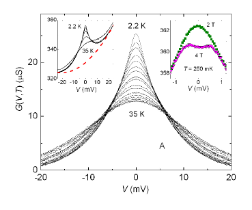
The left inset to Fig. 1 shows the raw data for the junction A at several temperatures between 2.2 and 35 K. One clearly sees conductance peaks around zero bias voltage, sitting on an asymmetric, parabolic background BDR1970 . After subtracting this parabolic background, the excess conductance contains a dominant even contribution and a minor odd contribution , where Yeh-thesis . In this work, we focus on the even contribution and denote it as . The main panel of Fig. 1 indicates that, as reduces, the curves become narrower and the peaks higher. Such enhanced cannot be expected from the disorder-induced suppression of electronic density of states at the Fermi level due to the electron-electron interaction effects WAL95 .

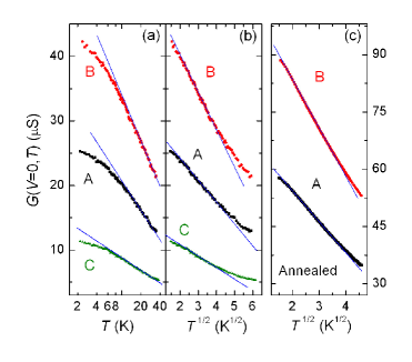
The magnitudes of the zero-bias conductance for junctions A–C are plotted in Fig. 2. At higher temperatures ( 16–32 K), obeys a ln law [Fig. 2(a)], suggesting a Kondo-like mechanism. Notably, in our intermediate temperature regime of 5–16 K, for all three samples obey a law [Fig. 2(b)], while a deviation from the dependence starts at about 4 K. We first notice that, in the high regime, both the behavior as well as our measured finite-bias spectra Yeh-thesis can be well described by a perturbative theory that considers the – exchange coupling between tunneling electrons and isolated localized moments which reside slightly inside the barrier Appelbaum1967 . This observation firmly establishes the fact that localized moments are present in our oxide barriers. The formation of localized moments in our junctions most likely arose from the diffusion of some 3 Sc atoms slightly into the AlOx barrier, e.g., during the fabrication process Wyatt1974 .

It is known that in the 2CK state the conductance due to electrons tunneling through an individual 2CK impurity residing in the barrier can be expressed by Affleck93 ; Hettler1994 ; Pustilnik2004 , where and are nonuniversal constants which may depend on the distance of the 2CK impurity from the electrode/barrier interface. is a universal scaling function of with the asymptotes for , and for , with 0.0758 Affleck93 ; Pustilnik2004 . For macroscopic junctions, there may be a number of 2CK impurities situating inside the barrier. If the interaction between these 2CK impurities can be neglected, the total conductance is additive: , where . Therefore, the zero-bias conductance has a dependence. To eliminate , which cannot be measured directly, it is very useful to scale the conductance as a universal function of : . This universal function leads to the asymptotes:
| (3) |
where , , and . In the low bias region (), the conductance can also be scaled into the form
| (4) |
where .

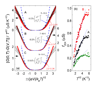
The behavior of in Fig. 2(b) suggests that our junctions fall in the 2CK phase in this intermediate temperature regime. In order to establish more and stronger evidences for this result, we have examined the scaling behavior of the finite bias conductance . Our measured conductances at various temperatures are scaled according to the 2CK scaling form, Eq. (3), and the results are shown in Fig. 3(a). Notice that at intermediate temperatures ( 5–16 K), the data at different all collapse onto a single curve for , with the asymptotes correctly given by Eq. (3). That is, our scaled at low bias voltages of comment1 , while it varies linearly with at high bias voltages. Therefore, the observed law together with the scaling behavior of the unambiguously demonstrate that our junctions fall in a 2CK state in this intermediate temperature regime. The prefactor in Eq. (4) can be extracted from the low bias data, and is plotted in Fig. 3(b). It shows that at intermediate temperatures, but deviates at high and low temperatures. This 2CK temperature regime for is in good accord with that found in Fig. 2(b) for the attribute.
In the high temperature end, since the deviation of from the law starts at Hettler1994 , the two-channel Kondo temperature, , for our junctions may be evaluated. In the low temperature end, there is a crossover temperature, , below which deviates from the law. Our values of and are listed in Table 1. It should be noted that, in Fig. 3(a), deviations (red dotted lines) from the 2CK scaling form are seen for data with 3.6 K.
The effect of a magnetic field is shown in the right inset to Fig. 1. We have found decreases with increasing , and observed a Zeeman splitting of 0.45 meV at 4 T. Such a Zeeman splitting corresponds to a -factor of 1.94, strongly indicating the presence of localized spin- moments, as discussed above. Thus, our observed logarithmic and 2CK behaviors of can be explained as arising from the Sc -electron impurities. The 2CK physics in our junctions should not originate from any TLS-induced effect, since the behavior in our junctions remained intact even after thermal annealing anneal , as is depicted in Fig. 2(c). In contrast, we notice that the 2CK signals in the above-mentioned ultrasmall metal point contacts disappeared even after annealing at room temperatures Ralph1992 . On the other hand, the two-channel magnetic Kondo model developed to explain the Ce-based heavy fermion compounds should require very special symmetries in the crystal field Zawadowski1998 , which are unlikely to happen in our junctions. Yet, another possible candidate theory is the competition between the Kondo screening and the interimpurity interaction proposed in the two-impurity Kondo model (2IKM) Jones1988-1989 ; Zarand2006-Chung2007 , where the 2CK physics occurs at a critical coupling strength , which separates a Kondo-screened phase from a local-singlet phase in the ground state. However, the existence of the 2CK fixed point due to the 2IKM coupled to a single electron reservoir requires some particle-hole symmetry Jones1988-1989 ; Zarand2006-Chung2007 which is hard to conceive in our junctions. Thus, the microscopic origin for our observed 2CK behavior as well as the deviation from the 2CK behavior below about 4 K is still not well understood in terms of available theories.
On the experimental side, it is intriguing that our 2CK effect is demonstrated in conventional planar tunnel junctions which contained 3 transition-metal impurities. These are straightforward sample structures, equipped with the simplest possible dynamical impurities () for the Kondo phenomena Hewson . Moreover, it should be noted that a deviation from the 2CK behavior has not been found in any previous experiments involving more exquisite artificial structures, such as metal point contacts Ralph1994 and semiconductor quantum dots Potok2007 , where the characteristic Kondo temperatures are relatively low, as compared with ours. The deviation could signify a crossover to a non-2CK phase as 0 K. This issue deserves further investigations.
In summary, the 2CK non-Fermi liquid physics has been realized in the differential conductances of Al/AlOx/Sc planar tunnel junctions. In the intermediate temperature regime, reveals a dependence and obeys the 2CK scaling law. At lower temperatures, a deviation in from the behavior is found. These rich Kondo behaviors are believed to originate from a few localized spin- Sc atoms situating at or slightly inside the AlOx/Sc interface.
Acknowledgements.
The authors thank A. M. Chang, C. H. Chung, T. A. Costi, D. L. Cox, F. Guinea, T. K. Ng, J. Kroha, Z. S. Ma, G. Zarand, and A. Zawadowski for helpful discussions. This work was supported by the Taiwan National Science Council through Grant No. 96-2112-M-009-025 and by the MOE ATU Program.References
- (1) A. C. Hewson, The Kondo Problem to Heavy Fermions (Cambridge University Press, Cambridge, 1993).
- (2) P. Nozières and A. Blandin, J. Phys. (Paris) 41, 193 (1980).
- (3) D. L. Cox and A. Zawadowski, Adv. Phys. 47, 599 (1998).
- (4) B. Andraka, Phys. Rev. B 49, 3589 (1994); T. S. Kim and D. L. Cox, Phys. Rev. Lett. 75, 1622 (1995).
- (5) H. R. Ott et al., Phys. Rev. Lett. 50, 1595 (1983); D. L. Cox, ibid. 59, 1240 (1987); C. L. Seaman et al., ibid. 67, 2882 (1991).
- (6) A. Zawadowski, Phys. Rev. Lett. 45, 211 (1980); A. Muramatsu and F. Guinea, ibid. 57, 2337 (1986).
- (7) D. C. Ralph et al., Phys. Rev. Lett. 72, 1064 (1994).
- (8) R. M. Potok et al., Nature 446, 167 (2007); A. I. Tóth et al., Phys. Rev. B 76, 155318 (2007).
- (9) Y. Oreg and D. Goldhaber-Gordon, Phys. Rev. Lett. 90, 136602 (2003).
- (10) T. Cichorek et al., Phys. Rev. Lett. 94, 236603 (2005).
- (11) A. F. G. Wyatt, J. Phys. C 7, 1303 (1974).
- (12) J. A. Appelbaum, Phys. Rev. 154, 633 (1967); E. L. Wolf and D. L. Losee, Phys. Rev. B 2, 3660 (1970). This theory predicts an approximation form , where and are constants, , and is a cutoff energy.
- (13) S. S. Yeh, Ph.D. dissertation, National Chiao Tung University (Taiwan, 2007).
- (14) J. M. Rowell, in Tunneling Phenomena in Solids, edited by E . Burnstein and S. Lundqvist (Plenum, New York, 1969).
- (15) The background resulted from normal tunneling between two metal electrodes separated by a thin barrier. W. F. Brinkman et al., J. Appl. Phys. 41, 1915 (1970).
- (16) N. S. Wingreen et al., Phys. Rev. Lett. 75, 769 (1995).
- (17) I. Affleck and A. W. W. Ludwig, Phys. Rev. B 48, 7297 (1993).
- (18) M. H. Hettler et al., Phys. Rev. Lett. 73, 1967 (1994).
- (19) M. Pustilnik et al., Phys. Rev. B 69, 115316 (2004).
- (20) Y. Oreg and D. Goldhaber-Gordon, in Physics of Zero- and One-Dimensional Nanoscopic Systems, ed. S. N. Karmakar et al. (Springer, Berlin, 2007).
- (21) Recent numerical calculations Hettler1994 indicate the scaled conductance even for .
- (22) Thermal annealing of the junctions was performed in vacuum ( 10-5 torr) at 100∘C for 1 h. After annealing, the (300 K) of samples A and B decreased to 0.83 and 0.50 k, respectively. In ploting Fig. 2(c), the background conductances had been subtracted.
- (23) D. C. Ralph and R. A. Buhrman, Phys. Rev. Lett. 69, 2118 (1992).
- (24) B. A. Jones et al., Phys. Rev. Lett. 61, 125 (1988); J. Gan, ibid. 74, 2583 (1995).
- (25) G. Zarand et al., Phys. Rev. Lett. 97, 166802 (2006); C. H. Chung and W. Hofstetter, Phys. Rev. B 76, 045329 (2007).