An electron Talbot interferometer
Abstract
The Talbot effect TAL36 , in which a wave imprinted with transverse periodicity reconstructs itself at regular intervals, is a diffraction phenomenon that occurs in many physical systems. Here we present the first observation of the Talbot effect for electron de Broglie waves behind a nanofabricated transmission grating. This was thought to be difficult because of Coulomb interactions between electrons and nanostructure gratings, yet we were able to map out the entire near-field interference pattern, the “Talbot carpet”, behind a grating. We did this using a Talbot interferometer, in which Talbot interference fringes from one grating are moiré-filtered by a 2nd grating. This arrangement has served for optical PAT89 , X-ray MKS03 , and atom interferometry CEP95 , but never before for electrons. Talbot interferometers are particularly sensitive to distortions of the incident wavefronts, and to illustrate this we used our Talbot interferometer to measure the wavefront curvature of a weakly focused electron beam. Here we report how this wavefront curvature demagnified the Talbot revivals, and we discuss applications for electron Talbot interferometers.
Electron optics is a highly developed field, but Talbot interferometry with electrons is new. In transmission electron microscopy Talbot revivals (Fourier self-images) behind crystals have been imaged directly, and understanding these revivals is necessary for the correct interpretation of crystal strucuture SPE03 . However, direct images of Talbot revivals are not nearly as sensitive to wavefront distortions as the signal from a Talbot interferometer. As we discuss, our arrangement of two nanogratings can easily detect a beam convergence of radians. Nanogratings have been used recently to construct other types of electron interferometers - a Lau type CRM06 and a Mach-Zehnder type GBB06 - but both of these designs are insensitive to wavefront deformations in the incident electron beam.
Observations of the Talbot effect with atoms CEP95 ; NKD97 launched many applications for near-field atom optics, such as compound beam splitters for atomic de Broglie waves WAW05 ; GDS06 , Talbot-Lau interferometers for atoms and large molecules CLL94 ; BHZ02 , interferometry with the Poisson spot for atom waves NSM98 , and “direct deposit” lithography of atoms behind phase and absorption gratings TBB92 ; MSC93 . Talbot interferometers have found numerous applications in light optics too, such as imaging phase objects LOS71 , measuring beam collimation SIL71 , and characterizing lenses BHA91 . For a review see PAT89 . Recently, nanostructures have been used to build X-ray Talbot interferometers MKS03 ; WCZ05 , which provide images of phase objects with less X-ray dose delivered to the subject. Imaging phase objects is possible because the Talbot interferometer is a type of shearing interferometer BAT47 ; RON64 , in which a beam is split into multiple overlapping paths. These applications, which which have been realized with atoms or photons, suggest potential uses for electron Talbot interferometers.
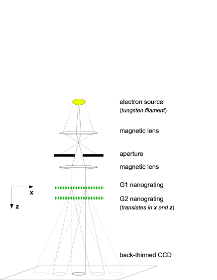
A diagram of our Talbot interferometer is shown in Figure 1. The nanofabricated gratings have a period 100 nm and serve as Ronchi rulings for low energy (10 keV) electrons MPC06 . When grating G1 is illuminated by collimated plane waves with wavelength , Fourier images (Talbot revivals) of the grating occur at half-integer multiples of the Talbot distance . For 2.8 keV electrons, 23 pm and 0.86 mm. The spatial modulations of these images, 100 nm in this case, are too small to resolve with our imaging detector, but they can be analyzed using a second grating G2.
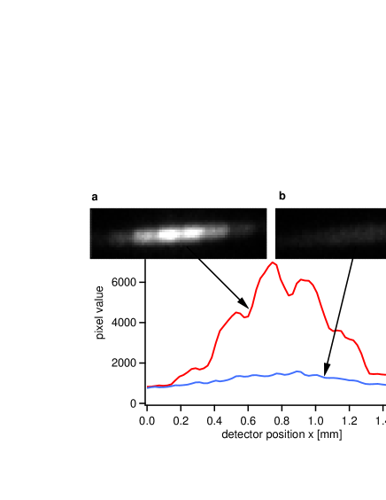
The total flux of collimated electrons transmitted to the far-field is maximum when the slits of G2 line up with the fringes of a Talbot revival from G1, as shown in Figure 2(a). In Figure 2(b) the transmitted flux is reduced by 77% when G2 is shifted laterally by half a period, since the Talbot fringes are then blocked by G2’s grating bars. This modulation of the total transmitted intensity (shown in Figure 2) occurs only when the gratings are illuminated by the plane waves of a well-collimated beam.
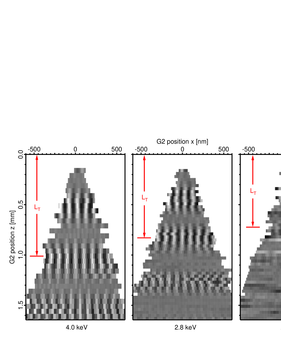
Images of the entire electron near-field interference pattern behind nanograting G1, also known as Talbot carpets, are shown in Figure 3. These data were obtained by scanning the position of analyzing grating G2 throughout the near-field region of G1, in both the and directions, while recording the total transmitted electron intensity. The tapered shape of each image is due to the limited lateral scan range at small G1-G2 separations.
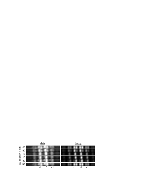
When G1 is illuminated with a converging beam, a different type of modulation is observed (Figure 4). In this condition, the Talbot revivals from G1 have a finer spatial period than the reference grating G2, due to geometrical demagnification by converging spherical wavefronts. As illustrated in a simulation shown in Figure 5, G2 blocks some parts of the beam but not others; i.e. there is a moiré effect between G2 and the interference pattern from G1. This causes dark spots to appear within the resolved far-field diffraction orders. When G2 is scanned laterally, these dark nulls move sideways through the diffraction pattern, as shown in Figure 4. This behavior is well-described by a general theoretical model that we developed for grating interferometers MCC08 . The only free parameter in this simulation was the radius of wavefront curvature of the incident beam. The theory (right column in Figure 4) matches the data (left column) best using an incident radius of wavefront curvature equal to m, corresponding to a nearly-collimated beam with a convergence angle of 75 rad. Negative diffraction orders in Figure 4 have a higher intensity than their positive counterparts, and this asymmetry is understood to result from image-charge (Coulomb) interactions between the grating and transmitted electrons MPC06 .
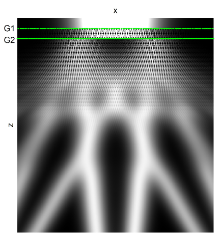
This work shows that the Talbot effect is a way to reproduce periodic structures using electron beams. Similar gratings have been used as masks for projection electron lithography YOS02 . However, deliberate use of the Talbot effect for lithography would be advantageous because the mask could be located millimeters from the substrate, since a Talbot revival, not a direct shadow, would be used for the exposure. Furthermore, as we have shown here, demagnified Fourier images created using a focused electron beam could be used to construct structures with finer periods than the original (a similar technique has already been demonstrated using UV lithography YMP99 ).
To summarize, we have built a Talbot interferometer for 2.8 keV electrons using two nanofabricated gratings. We used this device to map the near-field interference pattern, known as the Talbot carpet, behind a single grating. Analogous to X-ray and optical Talbot interferometers, this arrangement is very sensitive to deformations in the wavefronts of incoming electrons. We demonstrated this by measuring the 2.1-meter radius of wavefront curvature of a focused electron beam, and creating demagnified Talbot revivals with features smaller than the original grating. Both the imaging and lithographic capabilities afforded by the scaled Talbot effect will be explored in future work.
I Methods
The gratings were made by the NanoStructures Laboratory at MIT using achromatic UV interferometric lithography SSS96 , and are notable for their long range spatial coherence over a large (0.5 5 mm) area. They consist of an array of 50-nm-wide slits etched all the way through a 150-nm-thick suspended membrane of low stress Si3N5. The distance between adjacent slits, the grating period, is 100 nm. To enable their use as a diffractive optic for electrons, the gratings were sputter-coated with approximately 4 nm of Pt to prevent charging. Both gratings were identically prepared in the same batch process.
The electron beam was provided by a standard SEM electron optics column GNJ03 featuring a tungsten hairpin filament source. The column was adjusted to produce an approximately collimated, Ø150 m electron beam. The two gratings were mutually aligned about the optical () axis of the beam using a motorized rotation stage. The separation distance between the gratings was adjusted in 30 m steps from 0.1 to 1.7 mm using a motorized translation stage. For each separation distance, the gratings were shifted laterally (in the direction) with respect to the each other by tilting the mount that held them about an axis parallel to the gratings bars. An imaging detector placed 1 m downstream from the gratings collected images of the transmitted electrons, shown in Figures 2 and 4. To create the converging beam for the demagnified Talbot effect (Figure 4), a magnetic lens before the gratings was used to weakly focus the electron beam.
The electron detector is novel. A Princeton Instruments PIXIS-XO camera designed for X-ray and EUV imaging was used to directly image low energy (0.3-5 keV) electrons with high sensitivity. Back-thinned, back-illuminated CCDs have been used to directly detect low energy electrons before HOR03 , but to our knowledge this work is the first time a commercially-available camera has been used to directly image electrons.
Near-field interference fringes were revealed by moving G2 with respect to G1 in the and directions. The total transmitted electron flux was determined for each position of G2 by summing the value of all the pixels in images such as Figure 2(a). In total, 5200 images were acquired over a period of 3 hours (only 260 seconds of beam time was needed) to create the Talbot carpets in Figure 3. Each row in Figure 3, which corresponds to a particular grating separation, was shifted after the data were acquired so that intensity peaks in adjacent data sets lined up. This was necessary because small displacements (of order 50 nm) in were unavoidable while shifting the separation by hundreds of microns.
The simulations of the demagnified Talbot effect (in the right column of Figure 4 and in Figure 5) use a diffractive optical theory developed in MCC08 based on Gaussian Schell-model beams. Input parameters to the simulation in Figure 4 - such as the initial beam width, spatial coherence, and electrostatic interactions between transmitted electrons and the grating - were obtained in previous measurements MPC06 , and only the radius of wavefront curvature was left as a free parameter. The parameters used for the simulation in Figure 5 are not based on experiment - they were chosen in order to best illustrate the various interference phenomenon throughout the Talbot interferometer under focused illumination.
II Acknowledgements
We acknowledge Manjul Shah at Princeton Instruments for the loan of the PIXIS imaging detector, Tim Savas at MIT for fabricating the gratings, and Mark Robertson-Tessi and Grady Weyenberg for helping to construct the electron beam apparatus. This work was supported by the National Science Foundation Grant No. PHY-0653623, and by the University of Arizona.
III Competing financial interests
The authors declare no competing financial interests.
IV References
References
- (1) Talbot, H. F. Facts relating to optical science. Philosophical Magazine 9, 401–407 (1836).
- (2) Patorski, K. The self-imaging phenomenon and its applications. Progress in Optics 27, 3–108 (1989).
- (3) Momose, A. et al. Demonstration of x-ray talbot interferometry. Japanese Journal of Applied Physics Part 2-Letters 42, L866–L868 (2003).
- (4) Chapman, M. S. et al. Near-field imaging of atom diffraction gratings - the atomic talbot effect. Physical Review A 51, R14–R17 (1995).
- (5) Spence, J. C. H. High-Resolution Electron Microscopy (Oxford University Press, New York, 2003).
- (6) Cronin, A. D. & McMorran, B. Electron interferometry with nanogratings. Physical Review A 74, 061602(R) (2006).
- (7) Gronniger, G., Barwick, B. & Batelaan, H. A three-grating electron interferometer. New Journal of Physics 8, 224 (2006).
- (8) Nowak, S., Kurtsiefer, C., Pfau, T. & David, C. High-order talbot fringes for atomic matter waves. Opt. Lett. 22, 1430–1432 (1997).
- (9) Wang, Y. J. et al. Atom michelson interferometer on a chip using a bose-einstein condensate. Physical Review Letters 94 (2005).
- (10) Garcia, O., Deissler, B., Hughes, K. J., Reeves, J. M. & Sackett, C. A. Bose-einstein-condensate interferometer with macroscopic arm separation. Physical Review A 74 (2006).
- (11) Clauser, J. F. & Li, S. F. Talbot-vonlau atom interferometry with cold slow potassium. Phys. Rev. A 49, R2213–R2216 (1994).
- (12) Brezger, B. et al. Matter-wave interferometer for large molecules. Physical Review Letters 88, 100404 (2002).
- (13) Nowak, S., Stuhler, N., Pfau, T. & Mlynek, J. Charged wire interferometer for atoms. Physical Review Letters 81, 5792–5795 (1998).
- (14) Timp, G. et al. Using light as a lens for submicron, neutral-atom lithography. Physical Review Letters 69, 1636–1639 (1992).
- (15) McClelland, J. J., Scholten, R. E., Palm, E. C. & Celotta, R. J. Laser-focused atomic deposition. Science 262, 877–880 (1993).
- (16) Lohmann, A. W. & Silva, D. E. An interferometer based on the talbot effect. Optics Communications 2, 413–415 (1971).
- (17) Silva, D. E. Simple interferometric method of beam collimation. Applied Optics 10, 1980– (1971).
- (18) Bhattacharya, J. C. & Aggarwal, A. K. Measurement of the focal length of a collimating lens using the talbot effect and the moire technique. Applied Optics 30, 4479–4480 (1991).
- (19) Weitkamp, T. et al. X-ray phase imaging with a grating interferometer. Optics Express 13, 6296–6304 (2005).
- (20) Bates, W. J. A wavefront shearing interferometer. Proceedings of the Physical Society of London 59, 940– (1947).
- (21) Ronchi, V. 40 years of history of grating interferometer. Applied Optics 3, 437– (1964).
- (22) McMorran, B., Perreault, J. D., Savas, T. A. & Cronin, A. D. Diffraction of 0.5 kev electrons from free-standing transmission gratings. Ultramicroscopy 106, 356–364 (2006).
- (23) McMorran, B. & Cronin, A. D. Model for partial coherence and wavefront curvature in grating interferometers. Physical Review A 78, 013601 (2008).
- (24) Yoshizawa, M. & Savas, T. A. A feasibility study of 50 nm resolution with low energy electron beam proximity projection lithography. Japanese Journal of Applied Physics Part 2-Letters 41, L87–L88 (2002).
- (25) Yeh, W. H., Mansuripur, M., Fallahi, M. & Penner, R. S. Talbot imaging with increased spatial frequency: a technique for replicating truncated self-imaging objects. Optics Communications 170, 207–212 (1999).
- (26) Savas, T. A., Schattenburg, M. L., Carter, J. M. & Smith, H. I. Large-area achromatic interferometric lithography for 100 nm period gratings and grids. Journal of Vacuum Science and Technology B 14, 4167–4170 (1996).
- (27) Goldstein, J. I. et al. Scanning Electron Microscopy and X-Ray Microanalysis (Springer, New York, 2003).
- (28) Horacek, M. Charge-coupled device area detector for low energy electrons. Review of Scientific Instruments 74, 3379–3384 (2003).