Also at ]National Taras Shevchenko University of Kiev, Ukraine.
Design and optimization of one-dimensional ferrite-film based magnonic crystals
Abstract
One-dimensional magnonic crystals have been implemented as gratings of shallow grooves chemically etched into the surface of yttrium-iron garnet films. Scattering of backward volume magnetostatic spin waves from such structures is investigated experimentally and theoretically. Well-defined rejection frequency bands are observed in transmission characteristics of the magnonic crystals. The loss inserted by the gratings and the rejections bands bandwidths are studied as a function of the film thickness, the groove depth, the number of grooves, and the groove width. The experimental data are well described by a theoretical model based on the analogy of a spin-wave film-waveguide with a microwave transmission line. Our study shows that magnonic crystals with required operational characteristics can be engineered by adjusting these geometrical parameters.
pacs:
75.50.Gg, 75.30.Ds, 75.40.GbI introduction
Periodically structured magnetic materials such as magnonic crystals (MC) attract special attention in view of their applicability for both fundamental research on linear and nonlinear wave dynamics in artificial media, and for signal processing in microwave frequency range MC review . Similar to sound and light in sonic and photonic crystals, the dispersion characteristics of spin waves in magnonic crystals are strongly modified with respect to uniform media. This results in the appearance of frequency band gaps Nikitov ; BH Kolodin wherein spin-wave propagation is forbidden. A large variety of nonlinear spin-wave phenomena, as well as the dependency of the spin-wave properties both on the magnitude and orientation of a bias magnetic field determine the wide tunability of operational characteristics of the magnonic crystals and their potential for design of microwave filters, switchers, current controlled delay lines, power limiters, etc MC review .
Depending on the required insertion loss, operating frequency range, dimensions, temperature stability, and other performance specifications, periodic structures can be fabricated from either ferrite or ferromagnetic substances by means of geometric structuring MC review ; MC skyes ; MC MSSW ; MC FVMSW ; Gubbiotti1 ; Gubbiotti2 ; Ogrin ; blade , metal deposition metalization , ion implantation ionic implantation , local variations of the bias magnetic field field modulation , to name but a few.
At the present time, the smallest out-of-band insertion loss in conjunction with the deepest rejection bands have been observed in the experiments with geometrically structured yttrium-iron-garnet (YIG) single crystal ferrite films grown on a gallium-gadolinium substrate by means of liquid-phase epitaxy. In this unique material Saga the lifetime of spin-wave excitations can exceed a couple of hundreds nanoseconds, and the spin-wave propagation path reaches a few centimeters.
The surface magnetostatic waves Damon-Eshbach (wave propagation direction is perpendicular to the magnetic field applied in the film plane) and the forward magnetostatic waves Damon-VanDeVaart (external field is oriented perpendicular to the film plane) were previously studied theoretically and experimentally in such periodical structures MC review ; MC skyes ; MC MSSW ; MC FVMSW .
In our recent paper APL_MC we presented the first experimental and theoretical results on scattering of backward volume magnetostatic waves (wave propagation direction is parallel to the magnetic field applied in the film plane) Damon-Eshbach from an one-dimensional structure with periodic changes of the YIG film thickness.
In the present paper we present a detailed study of this kind of magnonic crystal. Its main characteristics, such as insertion loss in the rejection bands, parasitic loss in the transmission bands, and the frequency bandwidth of the rejection bands, were investigated for crystals having different groove depths, widths, and groove numbers. Our results show these parameters can be used to optimize the design of magnonic crystals.
II technology and experimental measurements
To fabricate magnonic crystals, 5.5 m and 14 m-thick YIG films, which were epitaxially grown in the (111) crystallographic plane, were used. Photolithographic patterning followed by hot orthophosphoric acid etching was used to form the grooves. The lithography was based on a standard photoresist AZ 5214E hardened by UV irradiation and baking which makes it stable against hot 160 oC orthophosphoric acid. Using this procedure we patterned arrays of parallel lines ( and ) of widths m and interline spacings of 270 m. Alternatively, arrays where m spaced by 290 m were also prepared. In all cases, the lattice constant was m. The grooves were transversely oriented with respect to the spin-wave propagation direction. In order to study the dependence of crystal characteristics on the groove depth the grooves were etched in 100 nm steps from 100 nm to 2 m. The groove depth was controlled by the etching time (etch rate was m/min) and measured using a profilometer. Anisotropic chemical etching of the YIG crystal structure by orthophosphoric acid etching was observed: the etch rate parallel to the film plane was approximately ten times larger than in the perpendicular direction, so the final groove depth profile along the direction of wave propagation had a trapezoidal shape.
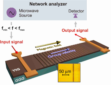
The inset in Fig. 1 shows the microscope image of the grooves structure of the magnonic crystal with the groove depth nm and groove width m. Anisotropic etching can be clearly seen.
In order to excite and receive the dipolar spin waves, two microstrip antennas were placed 8 mm apart, one in front of the grating, and one behind it (see Fig. 1). A bias magnetic field of 1845 Oe was applied in the plane of the YIG film stripe, along its length and parallel to the direction of spin-wave propagation. Under these conditions, backward volume magnetostatic wave (BVMSW) propagation occurs. A continuous-wave microwave signal was applied from a network analyzer (see Fig. 1) to the input antenna, and BVMSW transmission characteristics were measured. The microwave signal power was maintained at 1 mW in order to avoid any non-linear processes.
III Theoretical model
In a general case, a theoretical description of the scattering of dipole spin waves from inhomogeneities is given by a singular integral equation
| (1) |
where is the dynamic magnetization, is the microwave field of the input antenna, is the Green’s function of dipole magnetic field, and is the tensor of the microwave magnetic susceptibility which depends on the spin-wave carrier frequency and on the magnetic parameters of the film. The latter are functions of the position , since the grooves induce inhomogeneity in the internal static field and in the equilibrium magnetization . The integration is carried over the volume of the magnetic structure, thus the inhomogeneity of the film thickness is taken into account. A simple approximate solution to Eq.(1) for the reflected wave can be obtained in the frame of the first Born approximation (see kostylev for details of the approach). Neglecting magnetic damping in the medium far in front of the groove lattice for the complex reflection coefficient , one obtains
| (2) |
where for , where is the wavenumber of the incident spin wave, is the unpatterned film thickness, is the groove depth, is the groove width, is the lattice period, and is the total number of grooves in the groove lattice. This formula is in agrement with Bragg’s diffraction law. The maxima of reflection occur at or for the wavelengths . With increasing the depth of the reflection bands increase and their wavenumber widths decrease. Furthermore, the reflection grows with an increase in and , which is consistent. However, according to this formula, the reflection should decrease with increasing , which is in contradiction with the experimental results presented here (see Section IV). Thus a more detailed model is necessary.
To build a more appropriate model, we first notice that the quasi-1D dipole field guslienko of the lowest BVMSW thickness mode decays within a distance of a few film thicknesses from its source. Because the width of the grooves is much smaller than , the spin wave travels as an eigenmode of a continuous film of thickness through most of the lattice (i.e. between grooves). For the sections where the thickness is the integral equation reduces to a simple formula (see Eq. (50) in kostylev ) which shows that between the grooves, the transmitted and reflected waves only accumulate phase and decay (due to intrinsic magnetic damping). Thus, in order to describe the formation of stop bands, one has to consider the scattering of a BVMSW from just one groove. The effect of multiple consecutive grooves is obtained by cascading the structure period using matrices of scattering T-parameters and taking interference effects into account.
The most direct way to proceed is to solve this two-dimenstional singular integral equation numerically to obtain the scattering characteristics of a BVMSW scattering from a single groove. However this work is beyond the scope of this paper. Another way to treat scattering from a single groove was previously suggested in Refs. kalinikos ; Maeda . In our short paper APL_MC , we adapted this method to the case of a BVMSW. For completeness, we reproduce our theory here, but in more detail. We first consider the grating as a periodical sequence of sections of regular transmission lines with different propagation constants (different spin-wave wavenumbers) for the same carrier frequency. We neglect the fact that the groove edges are oblique, and consider the groove cross-section as a rectangle with the same depth and having the same area. In order to describe spin wave transmission through the magnonic crystal we use T-matrices which describe the relation between the amplitudes of the wave incident onto an inhomogeneity and reflected from it transm line . The T-matrix for a section of unstructured film (section of film between neighboring grooves) of length has diagonal components only:
| (3) |
where is the spin-wave wavenumber in the unstructured film, is the rate of the spin-wave spatial damping, is the gyromagnetic ratio, is the ferromagnetic resonance linewidth, and is the spin-wave group velocity.
Similarly, the T-matrix for a regular spin-wave film waveguide with a thickness is
| (4) |
where is the spin-wave damping rate for the groove. Here we use the fact that the BVMSW dispersion law for small wavenumbers is practically linear. Therefore, the spin-wave wavenumber in the grooves is . To describe the loss increase in the pass bands with increasing groove depth, we introduce an empirical parameter which accounts for larger contribution of two-magnon scattering processes in the areas which underwent anisotropic etching etching . Then the damping rate in the grooves can be expressed as .
At the edges of the grooves the incident wave is partially reflected back. This is accounted for by the T-matrices for the groove edges. The matrix for the front edge is , and that for the rear edge is . Following transm line , the transmission coefficient through the junction is . Then one obtains:
| (5) |
| (6) |
Using the property of T-matrix multiplication one finds a T-matrix for one period of the structure:
| (7) |
To obtain the T-matrix for a magnonic crystal with grooves , one has to raise to the -th power:
| (8) |
The most important operational parameter of magnonic crystals is the power transmission coefficient. It can be determined as , where and are the matrix elements.
In order to make use of this theory, one has to specify the form of the reflection coefficient . The model we suggest is based on the analogy of the change in the film waveguiding properties to a change in the characteristic impedance of a microwave transmission line kalinikos . The expression for the complex reflection coefficient for a junction of two microwave lines with characteristic impedances and can be written as transm line :
| (9) |
We assume that the change of the characteristic impedance of a spin-wave waveguide arising from the change of YIG-film thickness is due to a change of the film’s effective inductance. Then the characteristic impedance is linearly proportional to the propagation constant (to the spin-wave wavenumber in our case), and we obtain a formula for the reflection coefficient for a wave incident onto the edge of a groove from the unstructured section of the film:
| (10) |
where is a phenomenological parameter introduced in this formula to account for eventual factors which were not taken into account in this simplistic model.
For the wave incident onto the same junction in the reverse direction, , which has already been taken into account in the expressions for the T-matrices above. The expression means that the wave phase change due to reflection from one and another edge of groove is .
IV Results and discussion
The experimental BVMSW transmission characteristics for the unstructured film and for the magnonic crystals with = 300, 600 and 900 nm measured with a network analyzer are shown in Fig. 2(a). The initial YIG film thickness is 5.5 m. The results are shown for the groove number and the groove width m. The BVMSW transmission characteristic for the unstructured film has a maximum just below the point of ferromagnetic resonance. One sees that the insertion loss is dB and is determined by the energy transformation efficiency by the input and the output antennas and by the spatial decay of spin waves during their propagation in the space between the antennas. As BVMSW frequency band is bounded above by the ferromagnetic resonance frequency no spin-wave propagation occurs for higher frequencies. With decreasing frequency the BVMSW excitation and reception efficiencies drop. This drop is due to the finite width of the antennas in the direction of BVMSW propagation. Thus for very low and very high frequencies, no spin waves can be excited and the insertion loss ( dB) is determined by the direct electromagnetic leakage from the input to the output antenna. A small separate peak at the right-hand edge of the transmission characteristic is due to excitation of the first width standing mode of film width mode .
In order to remove the influence of the antennas and of the spin-wave spatial decay we calculate the difference between the logarithms of the transmission characteristics for the unstructured and the structured films. Figure 2(b) shows the obtained dependence. The additional dotted straight line in this figure indicates the limit of the dynamic range of our experimental setup. The latter is found as the difference in the transmission characteristics of the microstrip antenna structure that is covered or uncovered by a continuous YIG film.
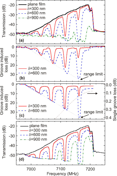
From Fig. 2(b) one sees that a lattice of 20 grooves as deep as 300 nm leads to the appearance of a set of rejection bands (or transmission gaps), where spin-wave transmission is highly reduced. According to the condition for Bragg reflection, higher-order rejection bands correspond to larger spin-wave wavenumbers. In the case of BVMSWs, the latter corresponds to lower frequencies. From the depths and the frequency widths of the gaps, one sees that the efficiency of the rejection increases with increasing order of Bragg reflection. This suggests that BVMSW with smaller wavelengths are more sensitive to the introduced inhomogeneities.
Both Fig. 2(a) and 2(b) demonstrate that an increase in leads to an increase in the rejection efficiency and in the frequency width of rejection bands . Additionally, a small frequency shift of the minima of transmission towards higher frequencies is observed, as well as an increase in insertion losses in the transmission (i.e. allowed) bands. For nm the insertion loss in the whole spin-wave band is so important that almost no spin-wave propagation is observed (see Fig. 2(a)) for the film of 5.5 m thickness.
The results of our numerical computation of are shown in Fig. 2(c). One sees that this model provides qualitative agreement with all the experimentally observed trends. In particular, it correctly predict the observed increase in the rejection efficiency with increasing . The calculated efficiency of the rejection also increases with increasing rejection band order. In order to prove this we calculate the transmission characteristic for a structure which consists of only one 30 m wide and 300 nm deep groove (see the dash-dotted line in Fig. 2(c)). One sees that the efficiency of spin-wave reflection from one groove increases with increase in spin wave wavelength. It is worth noting that the transmission loss inserted by one groove is about 0.1 dB. Thus, almost all the energy of the spin waves is transferred through the groove. Only a very small part (about 3 %) is reflected back.
Fig. 2(c) shows that our computation gives the correct shape of the transmission characteristics. In particular, there is a good agreement with the frequency widths of rejection bands and in their frequency shifts upwards with increasing . Furthermore, the model properly describes the increase in the parasitic insertion loss in the transmission bands with increasing groove depth.
The calculated influence of the groove array on the transmission characteristic of the magnonic crystal is shown in Fig. 2(d). The presented curves were found as a difference of the experimental transmission characteristic for a plane film (bold line in Fig. 2(a)) and the calculated groove induced loss (Fig. 2(c)). As a result, Fig. 2(d) are a theoretical analogue to Fig. 2(a), where experimental results are presented. From comparison of the figures one can concludes that proposed theoretical model describes experimental results especially good for the small values of the groove depth. With increasing of the groove depth the disagreement increases because of the theoretical model limitations.
IV.1 Influence of the groove depth
The groove depth has a profound influence on the transmission characteristics of the fabricated magnonic crystals (see Fig. 2). In order to investigate this effect in Fig. 3 we plot the insertion loss for the first-order rejection band, its frequency width, and the parasitic loss in the first transmission band for magnonic crystals of different thicknesses and with different groove depths. The central frequency of the first-order gap is 7160 MHz. From Fig. 3 (a) one sees that the rejection efficiency strongly increases with increasing the relative groove depth . An increase in the parasitic loss in the transmission bands is also observed. By comparing the losses in the rejection and transmission bands, we can estimate the optimal value of . We define this optimum value as a situation in which rejection is efficient but parasitic loss is still small (around 3 dB). For both films we find an optimal value of .
Both our calculation and measurements for different film thickness show that parasitic losses in transmission bands are determined by the relative groove depth only. The situation with the rejection efficiency is more complicated. From Fig. 3 (a) it can be seen that the experimental dependencies are slightly different for different film thicknesses. For the same relative groove depth, rejection is larger for thicker films. However, with increasing this difference between films with different thicknesses diminishes, and for the largest values of the experimental dependencies for different thicknesses collapse. This suggests that the relative groove depth is the leading parameter for the magnonic crystal optimization.
It is worth noting that the behavior of the calculated curves is slightly different. This suggests that the accuracy of our simple theory decreases with increasing groove depth. Processes not taken into account in our model probably become more prominent with larger .
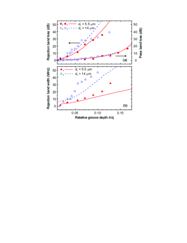
Fig. 3 (b) shows the experimental and calculated frequency width of the first rejection band. The frequency width was measured at the distance between the points for which the transmitted signal intensity is halved. Obviously, the same Bragg condition for the spin-wave number in the maximum of rejection is fulfilled for the magnonic crystals based on the films with thickness 5.5 m and 14 m, because the array has the same lattice constant 300 m in both cases. However, the spin wave dispersion strongly depends on film thickness Damon-Eshbach . For small wave wavenumbers its slope increases with increase in . This results in the wider rejection bands observed for the thicker magnonic crystal.
From Fig. 3 (b) one sees that the width of the rejection band for the optimal relative groove depth 0.1 is 15 MHz and 45 MHz for the 5.5 m and 14 m thick films, respectively. From the point of view of optimizing magnonic crystals, this gives an additional degree of freedom for designing a crystal which satisfied operational parameters. A required rejection-band bandwidth can be obtained by adjusting the magnon crystal thickness. The optimal rejection efficiency can be obtained by adjusting the relative groove depth.
From Fig. 3 (b) it follows that our theory is not very accurate. The agreement is qualitative only. However, considering the simplicity of our model, the agreement is satisfactory, and provides key trends.
IV.2 Influence of the number of grooves
The groove number is also important for the optimization of the magnonic crystal. Fundamentally, increasing the groove number should increase the efficiency of rejection.
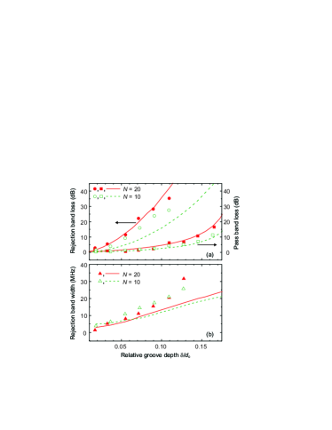
According to the developed theoretical model (see Eq. (8)), doubling the number of grooves should double the rejection losses on the log scale. In order to test this theoretical prediction, two crystals with the same geometry but having different grooves numbers and were investigated.
Fig. 4 presents the insertion loss and the frequency width of the rejection bands for the magnonic crystals with the groove numbers and , as a function of the relative groove depth . One sees that reducing the number of grooves by one half results slightly decreases the rejection efficiency. One of the possible explanation for such an experimental behavior could be a deviation from perfect periodicity in the lattice, which may saturate such dependence for groove numbers larger than some characteristic value. However, a careful examination of optical images of the quasi-crystal does not reveal any noticeable defects. As such, we suggest this unexpectedly weak dependence may be connected with some peculiarity of the intrinsic spin wave damping on the structure which is not taken into account in our model.
Fig. 4 (b) shows experimental and calculated frequency width of the first rejection band for the magnonic crystals with the groove numbers and , as a function of the relative groove depth. No pronounced dependence on the number of groove is observed.
IV.3 Influence of the groove width
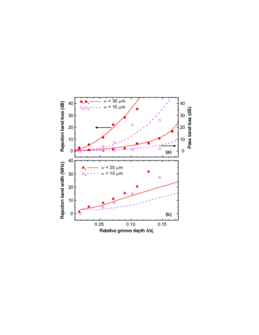
The groove width is also an important parameter in the design and optimization of magnonic crystals. In an ideal case, a Bragg reflector should consist of infinitely narrow reflectors, which are periodically placed in space. However, in our case infinitely narrow grooves will produce no reflection. Therefore one has to keep finite. As follows from Eq.(2) and from the T-matrix theory, an increase in the groove width increases the reflection coefficient of individual grooves. However, this obviously introduces out-of-phase reflections from the front and the rear edges of the grooves. Dephasing becomes more pronounced with increasing . (Indeed, such a structure can be modeled as a superposition of Braggs reflectors with three different lattice constants ( and ) and lattice origins which do not coincide in space.)
To investigate the impact of the groove width, a magnonic crystal with a groove width equal to the half of the lattice constant () was fabricated. A suitable model for such a structure should concept in a combination of four Bragg reflectors: two with a lattice constant , and the remaining two with lattice constant . Such a structure is characterized by the coincidence in the Bragg wavenumbers between the transmission resonances for the -period Bragg reflector and the reflection resonances for the -period reflection. Our additional experiment investigations proved this model: every even rejection band seen for a lattice of narrow (30 m wide) grooves are absent for the structure with .
Fig. 5 demonstrates the insertion loss (upper panel) and the frequency width (bottom panel) of the first rejection band (spin-wave wavelength here is around 600 m) for the magnonic crystals with groove widths m and m as a function of relative groove depth . One sees that tripling the groove width increases the rejection efficiency by approximately 4 times in the log scale. Almost the same effect is observed for the parasitic loss in the transmission band (see squares in Fig. 5(a)). One can see that the results of the calculation are in good qualitative agreement with the experiment.
In Fig. 5(b) experimental and calculated values for the width of the first rejection band are shown. One sees that for different groove widths, these plots are very close to one another. Even thought the difference is small, it may be sufficient to fine-tune the characteristics of the magnonic crystals and enable the obtention of required rejection efficiency and bandwidth of rejection bands.
V Conclusions
1. In this work we experimentally demonstrate that in the BVMSW configuration a one-dimensional magnonic crystal is characterized by the excellent spin-wave signal rejection of more than 30 dB. The efficiency of the rejection can be controlled by the groove depth and width as well as the number of grooves in the crystal. A simple theoretical model was proposed which is in good qualitative agreement with the experimental results.
2. It is found that the optimal groove depth which ensures strong rejection in the rejection bands while maintaining insertion loss in the transmission bands around 3 dB is approximately 1/10 of the total film thickness. Decreasing in the groove depth from this optimal value leads to a drop in the rejection efficiency. With its increasing parasitic loss in the transmission bands rapidly grows.
3. The efficiency of the rejection increases with an increasing number of grooves. However, this increase is smaller than our model’s prediction.
4. When the width of grooves is much smaller than the spin-waves wavelength, increasing the groove width leads to a fast increase in the rejection efficiency.
5. The width of the rejection bands for BMVSWs exceeds the values for the other spin-wave configurations MC review ; MC skyes ; MC MSSW ; MC FVMSW . It can be controlled by the film thickness and the groove depth. Varying the film thickness, groove depth, groove width and number of grooves allows the engineering of magnonic crystals with optimal characteristics.
Financial support by the DFG SE 1771/1-1, Australian Research Council, and the University of Western Australia is acknowledged.
References
- (1) K.W. Reed, J.M. Owens, R.L. Carter, Circ. Syst. Signal Process. 4, 157 (1985).
- (2) Yu.V. Gulyayev and S.A. Nikitov, Doklady Physics 46, 687 (2001).
- (3) P.A. Kolodin and B. Hillebrands, J. Magn. Magn. Mater. 161, 199 (1996).
- (4) C.G. Skyes, J.D. Adam, and J.H. Collins, Appl. Phys. Lett. 29, 388 (1976).
- (5) J.P. Parekh and H.S. Tuan, Appl. Phys. Lett. 30, 667 (1977).
- (6) J.P. Parekh and H.S. Tuan, IEEE Trans. Microwave Theory Tech. MTT-26, 1039 (1978).
- (7) M. Kostylev, P. Schrader, R. L. Stamps, G. Gubbiotti, G. Carlotti, A. O. Adeyeye, S. Goolaup, and N. Singh, Appl. Phys. Lett. 92, 132504 (2008).
- (8) G. Gubbiotti, S. Tacchi, G. Carlotti , N. Singh , S. Goolaup, A. O. Adeyeye , and M. Kostylev, Appl. Phys. Lett. 90, 092503 (2007).
- (9) M. Kostylev, R. Magaraggia, F. Y. Ogrin, E. Sirotkin, V. F. Mescheryakov, N. Ross, and R. L. Stamps, IEEE Trans. On Mag. 44, No. 10 (2008).
- (10) A. Maeda, M. Susaki, IEEE Trans. On Mag. 42, 3096 (2006).
- (11) J.M. Owens, J.H. Collins, C.V. Smith, Jr., and I.I. Chiang, Appl. Phys. Lett. 31, 781 (1977).
- (12) R.L. Carter, J.M. Owens, C.V. Smith, Jr. and K.W. Reed, J. Appl. Phys. 53, 2655 (1982).
- (13) Y.K Fetisov, N.V. Ostrovskaya and A.F. Popkov, J. Appl. Phys. 79, 5730 (1996).
- (14) V. Cherepanov, I. Kolokolov, V. L’vov, Physic Reports 229, 81 (1993).
- (15) R.W. Damon and J.R. Eshbach, Phys. Chem. of Solids 19 308 (1961).
- (16) R.W. Damon and H. Van De Vaart, J. Appl. Phys. 36, 3453 (1965).
- (17) A.V. Chumak, A.A. Serga, B. Hillebrands, M.P. Kostylev Appl. Phys. Lett. 93, 022508 (2008)
- (18) J. Basterfield, J. Phys. D: Appl. Phys. 2, 1159 (1969).
- (19) M.P. Kostylev, A.A. Serga, T. Schneider, T. Neumann, B. Leven, B. Hillebrands, and R.L. Stamps, Phys. Rev. B 76, 184419 (2007)
- (20) K.Yu. Guslienko, S.O. Demokritov, B. Hillebrands, and A.N. Slavin, Phys. Rev. B 66, 132402 (2002).
- (21) B.A. Kalinikos, private communication.
- (22) A. Maeda and M. Suzaki, IEEE Trans. on Mag., 42, 3096 (2006).
- (23) W. Berry, IEEE Trans. Microwave Theory Tech. MTT-34, 80 (1986).
- (24) M. P. Kostylev, G. Gubbiotti, J.-G. Hu, G. Carlotti, T. Ono, and R. L. Stamps, Phys. Rev. B, 76, 054422 (2007).