Two and One-dimensional Honeycomb Structure of Boron Nitride
Abstract
This paper presents a systematic study of two and one dimensional honeycomb structure of boron nitride (BN) using first-principles plane wave method. Two-dimensional (2D) graphene like BN is a wide band gap semiconductor with ionic bonding. Phonon dispersion curves demonstrate the stability of 2D BN flakes. Quasi 1D armchair BN nanoribbon are nonmagnetic semiconductors with edge states. Upon passivation of B and N with hydrogen atoms these edge states disappear and band gap increases. Bare zigzag BN nanoribbons are metallic, but become a ferromagnetic semiconductor when their both edges are passivated with hydrogen. However, their magnetic ground state, electronic band structure and band gap are found to be strongly dependent on whether B- or N-edge of the ribbon is saturated with hydrogen. Vacancy defects in armchair and zigzag nanoribbons affects also magnetic state and electronic structure. In order to reveal dimensionality effects these properties are contrasted with those of various 3D BN crystals and 1D BN atomic chain.
pacs:
73.22.-f, 75.75.+a, 63.22.-mI introduction
Synthesis of a single atomic plane of graphite, i.e. Graphene with covalently bonded honeycomb lattice has been a breakthrough for several reasons novo ; zhang ; berger . Firstly, electrons behaving as if massless Dirac Fermions have made the observation of several relativistic effects possible. Secondly, stable graphene has disproved previous theories, which were concluded that two-dimensional structures cannot be stable. Graphene displaying exceptional properties, such as high mobility even at room temperature, ambipolar effect, Klein tunelling, anomalous quantum hall effect etc. seems to offer novel applications in various fields graphene_applications1 . Not only 2D graphene, but also its quasi 1D forms, such as armchair and zigzag nanoribbons have shown novel electronic and magnetic properties graphene_applications2 ; graphene_applications3 ; graphene_applications4 , which can lead to important applications in nanotechnology. As a result, 2D honeycomb structures derived from Group IV elements and Group III-V and II-VI compounds are currently generating significant interest owing to their unique properties.
Boron-Nitride (BN) in ionic honeycomb lattice which is the Group III-V analogue of graphene have also been produced having desired insulator characteristics bn-synthesis . Nanosheets bn-nanosheets1 ; bn-nanosheets2 , nanocones bn-nanocones , nanotubes bn-nanotubes , nanohorns bn-nanohorns , nanorods bn-nanorods and nanowires bn-nanowires of BN have already been synthesized and these systems might hold promise for novel technological applications. Among all these different structures, BN nanoribbons, where the charge carriers are confined in two dimension and free to move in third direction, are particularly important due to their well defined geometry and possible ease of manipulation.
BN nanoribbons posses different electronic and magnetic properties depending on their size and edge termination. Recently, the variation of band gaps of BN nanoribbons with their widths and Stark effect due to applied electric field have been studied Guo ; louie-nanoletter . Recently the magnetic properties of zigzag BN nanoribbons have been investigated barone . Half-metallic properties have been revealed from these studies which might be important for spintronic applications. Production of graphene nanoribbons as small as 10 nm in width has been achieved dai1 ; dai2 and similar techniques are expected to be developed for BN nanoribbons.
A thorough understanding of 2D BN honeycomb structure and their various nanoribbons is important for further study of this graphene like compounds. BN by itself provides with very interesting chemical and physical properties, which may lead to important applications. In this paper, we present a detailed ab-initio study of electronic, magnetic and elastic properties of 2D (graphene like) BN and bare and hydrogen passivated, quasi 1D BN nanoribbons (BNNRs). We also investigated the effect of the vacancy defects on these properties. To reveal the dimensionality effects we include also a short discussion regarding 3D BN bulk crystals and 1D BN atomic chains. We found that 2D BN is a nonmagnetic, wide band gap semiconductor. The ionic bonding due to significant amount of charge from B to N atom opens a gap and hence dominates electronic structure. Calculated phonon dispersion curves provide a clear evidence that 2D BN flakes is stable. The armchair and zigzag nanoribbons of BN display even more interesting electronic and magnetic properties. Bare and hydrogen passivated armchair BN nanoribbons (A-BNNR) are nonmagnetic wide band gap semiconductor. The value of band gap of A-BNNR having width Å is practically independent from the width of nanoribbons. While the bare zigzag BN nanoribbons (Z-BNNR) are ferromagnetic metal, they become nonmagnetic semiconductor upon the passivation of both edges. We found that 2D BN and its nanoribbons have properties, which are complementary to graphene.
II Model and Methodology
We have performed first-principles plane wave calculations within density functional theory (DFT) using PAW potentials paw . The exchange correlation potential has been approximated by generalized gradient approximation (GGA) using PW91 pw91 functional both for spin-polarized and spin-unpolarized cases. All structures have been treated within supercell geometry using the periodic boundary conditions. A plane-wave basis set with kinetic energy cutoff of 500 eV has been used. In the self-consistent potential and total energy calculations the Brillouin zone (BZ) is sampled by special k-points. The numbers of these k-points are (15x15x15) for bulk BN, (25x25x1) for 2D BN and (25x1x1) for nanoribbons, respectively, and are scaled according to the size of superlattices. All atomic positions and lattice constants are optimized by using the conjugate gradient method, where the total energy and atomic forces are minimized. The convergence for energy is chosen as 10-5 eV between two steps, and the maximum Hellmann-Feynman forces acting on each atom is less than 0.02 eV /Å upon ionic relaxation. A large spacing ( 10 Å) between monolayers has been taken to prevent interactions between them. The pseudopotentials having 3 and 5 valence electrons for the B (B: ) and N ions (N: ) were used. Numerical calculations have been performed by using VASP package vasp1 ; vasp2 . The phonon dispersion curves are calculated within density functional perturbation theory (DFPT) using plane wave methods as implemented in PWSCF software pwscf .
III 3D BN Crystals and 1D atomic chain
In this section, we present our theoretical calculations on 3D bulk BN crystals and truly 1D BN atomic chain. Earlier these 3D bulk crystals BNcrystal1 ; BNcrystal2 ; BNcrystal3 ; BNcrystal4 ; BNcrystal5 and 1D atomic chains BNchain have been studied theoretically by using different methods. Our purpose in including these crystals of BN in different dimensionalities is to contrast their properties with those of 2D and quasi 1D honeycomb structures of BN and also reveal dimensionality effects.
III.1 3D Bulk BN crystals
Three dimensional bulk crystals include hexagonal-layered BN (h-BN), wurtzite BN (wz-BN) and zincblende BN (zb-BN) structures. Their atomic configurations and primitive unit cells are described in Fig. 1. By using the expression,
| (1) |
where E[BN] is the total energy per B-N pair of the optimized structure of BN crystal; E[B] and E[N] are the total energies of free B and N atoms; we calculated the equilibrium cohesive energies of h-BN, wz-BN and zb-BN crystals as -17.65, -17.45 and -17.49 eV per B-N pair, respectively. Accordingly, h-BN, which is the analogue of graphite, is the most energetic bulk structure. On the other hand, the cubic BN structure is known to be the second hardest material of all.
The lattice constants of the optimized structures in equilibrium are Å, and the distance between the nearest B and N atoms is Åfor h-BN layered crystal. For wz-BN, optimized values of , and are calculated to be 2.542 Å, 1.64, and 1.561 Å, respectively. The zincblende structure has lattice constant Å and Å. All our results related with the structural parameters are in good agreement with the experimental and theoretical values BNcrystal1 ; BNcrystal2 ; BNcrystal3 ; BNcrystal4 ; bulk-references within the average error of .
The calculated electronic band structure, total and partial (or orbital projected) density of states (DOS) of 3D crystals are presented in Fig. 1. These h-BN, wz-BN and zb-BN crystals are indirect band gap semiconductors with calculated band gaps being =4.47, 5.72, and 4.50 eV, respectively. The calculated values of differ from the earlier ones depending on the method used DFTgap . For h-BN having 2D BN atomic layers in the (x,y)-plane. The band structure is composed from the band structures of these individual atomic layers with hexagonal symmetry, which are slightly split due to weak coupling between them. Highest valence band has N- character; the states of the lowest conduction band is formed from B- orbitals (the z direction corresponds to “c” in Fig. 1 ). Overall features of the total density of states (TDOS) are similar for three 3D crystal structures. Valence band consists of two parts separated by a wide intra band gap. The lower part at -20 eV is projected mainly to N- and partly to N- and B- orbitals. The upper part is due to mainly N- and partly B- orbitals and has similarities in both zb-BN and wz-BN crystals. As for the lower part of the conduction band it is derived mainly from B- orbitals. The differences of three 3D crystals are pronounced in the lower part of the conduction band.
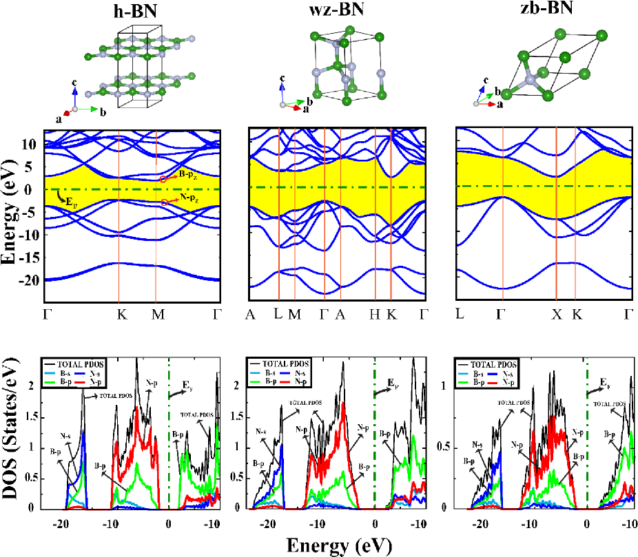
We calculate the amount of charge on constituent B and N atoms in 3D crystals by performing the Löwdin lowdin analysis in terms of the projection of plane-waves into atomic orbitals. By subtracting the valencies of free B and N atoms from the calculated charge values on the same atoms in 3D crystals we obtain the charge transfer, . The calculated values of for h-BN, wz-BN and zb-BN are 0.416, 0.342, 0.334 electrons, respectively. The fact that of zb-BN and wz-BN have almost equal values, but of h-BN crystal is significantly larger related to the shorter B-N bond length in h-BN crystal.
III.2 1D BN Atomic chain
BN forms stable segments of linear atomic chain BNchain like carbon tongay . This situation is in contrast to second and third row elements (such as Si and Ge) and III-V compounds and metals (such as Al, Au etc) which can form stable zigzag chain structures instead of linear chain structures. Our results on optimized chain structure yield the cohesive energy =16.04 eV per B-N pair, the B-N distance 1.307 Å, the indirect band gap E3.99 eV and charge transfer from B to N, 0.511 electrons. Hence the double bond between B and N is ionic.
IV 2D Honeycomb Structure of BN
Having discussed the overall structural and elastic properties of 3D and 1D BN, we now consider 2D BN with hexagonal symmetry. The atomic structure of 2D BN is similar to the honeycomb structure of graphene, except that the constituent atoms of the former are from III and V columns of the Periodic Table. Normally, the bond between nearest B and N atoms is formed from the bonding combination of B- and N- orbitals. However, owing to the electronegativity difference between B and N atoms electrons are transferred from B to N. As a result, in contrast to purely covalent bond in graphene the bonding between B and N gains an ionic character. The charge transfer from B to N dominates several properties of 2D BN including the opening of the band gap. In this respect the BN honeycomb structure is complementary to graphene.
IV.1 Charge density analysis and electronic structure
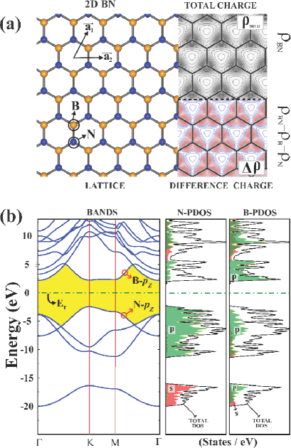
The atomic structure, atomic charge, charge transfer from B to N and the electronic structure of 2D BN are presented in Fig. 2. Contour plots of total charge indicates high density around N atoms. The difference charge density is calculated by subtracting charge densities of free B and N atoms from the charge density of 2D BN, i.e. . High density contour plots around N atoms protruding towards the B-N bonds indicate charge transfer from B to N atoms. This way the B-N bonds achieve an ionic character. The amount of transfer of charge is calculated by Löwdin analysis to be =0.429 electrons. Interestingly, is slightly larger than that calculated for h-BN, but significant larger than those calculated for wz-BN and zb-BN crystals.
2D BN is a semiconductor. Calculated electronic energy bands are similar to those calculated for h-BN crystal. The - and - bands of graphene which cross at the K- and K∗-points of the BZ open a gap in 2D BN as a bonding and antibonding combination of N- and B- orbitals. The contribution of N- is pronounced for the filled band at the edge of valence band. The calculated band gap is indirect and 4.64 eV. TDOS and partial density of states show also similarity to those of h-BN layered crystal presented in Fig. 1.
IV.2 Phonon spectrum
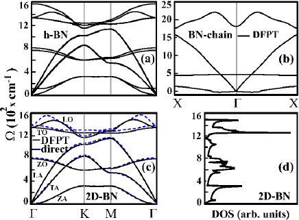
Even if the structure optimization resulting in the honeycomb structure in Fig. 2 can be taken as an indication for the stability of 2D BN, calculation of phonon dispersion curves through the diagonalization of dynamical matrix provides a more stringent test for stability. One of acoustical branches for to curves taking negative value even at a small region of BZ indicates the instability of the structure. There have been a number of experimental Rokuta and theoretical studies of phonon spectrum of 2D Wirtz and 3D honeycomb BN Kern ; Yu ; Serrano ; Solozhenkan ; Miyamoto . Here, the phonon dispersion curves of h-BN, 2D BN and 1D BN chain and density of states together with the infrared (IR) and Raman (R) active modes of 2D BN and h-BN at -point have been calculated by using density functional perturbation theory (DFPT) as implemented in PWSCF software pwscf . For the DFPT phonon calculation of bulk h-BN, we used a four atom primitive cell, which yield 12 phonon branches at the center of BZ in Fig. 3 (a). The symmetry point group is calculated as D6h (space group P6/mmm). The irreducible representations at is 2 E2g+ 2 B2g+2 A2u+2 E1u. While the modes E1u and E2g are doubly degenerate, B2g and A2u are non degenerate. The modes E1u and A2u are IR active, the E2g is Raman active. B2g is an inactive mode. Our results are in agreement with previously calculated and experimental data, but differ slightly from those of Serrano et al.Serrano . While present GGA calculations predict B2g mode as an inactive mode, LDA calculations by Serrano et al. found B1g as an inactive mode. Most of the phonon bands of h-BN are degenerate. This indicates that the coupling between BN layers in h-BN is weak. However, it is well known that the BN is polar material with long range dipole-dipole interaction. This gives rise to the splitting between longitudinal optical (LO) and transverse optical (TO) mode at point. The lowest transverse acoustical mode has parabolic dispersion as k 0 owing to rapidly decaying interatomic forces for transversal displacements decay . Another feature is the overlap of the lowest transversal optical mode with the acoustical modes.
In Fig. 3 (b) we show the phonon dispersion curve of BN atomic chain. Two TA modes have low frequency and get very small but negative values near the zone center. This indicates structural instabilty as . However, the linear segments of BN atomic chain can be stable. Similar to h-BN, the doubly degenerate TO branch overlaps with the LA branch.
For 2D BN honeycomb structure, the unit cell consists of two atoms. Accordingly, there are three acoustical and three optical branches in Fig. 3 (c). The symmetry point group is D3h (space group (P-62m)). Optical phonon modes at the -point is given by A+2 E. The mode A is IR active and the E mode is both IR and Raman active. The similarity between calculated phonon dispersion curves of h-BN and 2D-BN is remarkable.
We also calculate the phonon dispersion curves of 2D BN honeycomb structure by using PAW potentials paw as implemented in VASP vasp1 for further checking of the results of our phonon calculation. Force constants are determined from the supercells. The phonon modes were calculated by using the direct method as implemented in the PHON alfe software. The calculated phonon frequencies are almost identical with those calculated by DFPT method. In Fig. 3 (d), we present the phonon density of states calculated for 2D BN honeycomb structure. Note that both calculations yield that TA (or ZA) mode displaying parabolic dispersion gets negative frequencies as . similar to BN atomic chains, this indicates structural instability as . Accordingly, finite size of 2D BN flakes are expected to have stable structure.
V 1D BN Nanoribbons
Similar to graphene graphene-nanoribbons , two unique orientation in 2D BN yield nanoribbons with uniform edges: These are armchair (A-BNNR) and zigzag (Z-BNNR) nanoribbons. The profile of the atomic configuration at both edges of the nanoribbon determines their electronic and magnetic properties. The properties can be modified by the passivation of dangling bond of edge atoms by hydrogen. Because of their interesting electronic and spintronic properties, BN nanoribbons are attractive nanostructures for various device applications. Electronic properties of BN nanoribbons have been investigated in recent papers Guo ; louie-nanoletter ; barone . Present study is complementary to previous studies.
V.1 Electronic structure
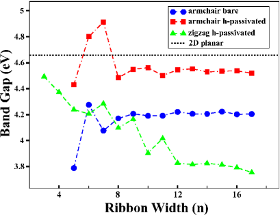
Here we present the results of our study on the electronic and magnetic properties of bare and hydrogen passivated A-BNNR and Z-BNNRs. Bare and hydrogen passivation A-BNNR are wide band gap semiconductors. Similarly, hydrogen passivated Z-BNNRs are also semiconductor. The band gaps of these BN nanoribbons depend on the width of the nanoribbons or the numbers of BN pairs, in the primitive unit cell. The variation of the band gap EG as a function of is given in Fig. 4. Normally, the properties of nanoribbons approaches to those of 2D honeycomb structure as the width . However, due to the localized edge states the band gap of Z-BNNR approaches to a gap smaller than that of 2D BN honeycomb structure louie-nanoletter . For narrow () bare and hydrogen passivated A-BNNRs the band gaps vary with , but they are practically unaltered for . For the band gap of bare A-BNNR is 0.4 eV smaller than that of hydrogen passivated A-BNNR. The band gap of hydrogen passivated Z-BNNR is 4.5 eV for , but decrease to 3.8 eV for . However, its variation with is not monotonic for , it rather display family dependent oscillatory variation with changes as large as 0.4 eV between two consecutive values of . On the other hand, bare Z-BNNRs are found to be metallic.
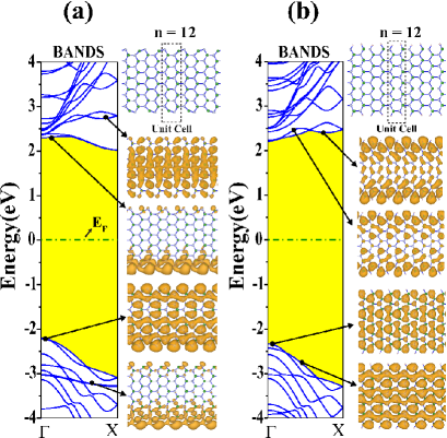
The atomic and electronic structure of bare and hydrogen passivated A-BNNR are described in Fig. 5 for . The atoms at the edges of the bare A-BNNR are reconstructed; while one edge atom, B is lowering, adjacent edge atom, N is raised. Two bands of edge states occur below the conduction band edge. These bands are normally degenerate for large , but split around the center of BZ due to their coupling. The bands of edge states occur -1 eV below the top of the valance band edge. Normal states, on the other hand, have charge distributed uniformly in the ribbon. Because of the edge states the band gap is indirect and is 4.22 eV wide. Upon passivation of the dangling bonds of B and N atoms situated at the edges with hydrogen atoms, these edge state bands are discarded from the band gap and reconstruction of edge atoms disappear. At the end, the band gap of H-passivated A-BNNR becomes direct and increases by 0.3 eV.
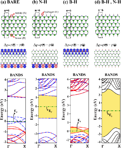
The electronic and magnetic states of Z-BNNR depend on whether their edges are passivated with hydrogen atoms. While a bare Z-BNNR is magnetic and metallic, it becomes nonmagnetic and a wide band gap semiconductor upon the passivation of B and N atoms at both edges. Moreover, its electronic and magnetic properties depend on whether only B- or N-side is passivated with hydrogen atoms. Accordingly, Z-BNNRs provide us for several alternatives for different electronic and magnetic properties barone . However, different magnetic states corresponding to different edge configuration, namely bare or hydrogen passivated, are very sensitive to the parameters of calculation. In Fig. 6 we present the calculated electronic structures of a Z-BNNR with =6 B-N pairs in a primitive unit cell for four different cases. These are both side free, only N-side is passivated with hydrogen, only B-side is passivated with hydrogen and both edges are passivated with hydrogen.
Bare Z-BNNR having both edges are free display different magnetic states (magnetic order), which are close in energy. Moreover, the ordering of these magnetic states with respect to their energy is sensitive to the criterion of energy convergence. To ensure the antiferromagnetic (AFM) order at edges, we considered double cells. The possible magnetic states are spin-up, spin-down for adjacent B atoms at one side and spin-up, spin-up for the adjacent N atoms at the other side; namely / spin configuration. Other possible spin configurations are / ; / ; / ; / . We found that the spin configuration, / for Z-BNNR having 12 B-N pairs in double unit cell corresponds to the ground state. The other excited configurations, / ; / ; / ; / , have 6,7,35,131 meV higher energies than ground state. The ordering of these configuration is slightly different from that reported earlier barone . Nevertheless, the difference between the earlier and present ground state energies are within the accuracy limits of DFT calculations. The ground state spin configuration / of the bare Z-BNNR having both edges free is found to be ferrimagnetic metal with per double cell. Whereas the excited magnetic state with configuration / is half metallic.
In Fig. 6 (b), Z-BNNR with N-edge passivated with hydrogen atoms is an AFM semiconductor. The AFM edge state is localized at the B-side. When only the B-side is passivated with hydrogen atoms the magnetic edge state is, this time, localized at the N-side of the ribbon. As seen in Fig. 6 (c) the ground state of Z-BNNR is ferromagnetic with =2 per double cell. Our calculations suggest that the nearest neighbor N-N interaction is ferromagnetic, the B-B interaction is antiferromagnetic. Finally, the Z-BNNR becomes non magnetic, when the atoms at both edges are passivated with hydrogen atoms. Earlier, Hwan and Louie louie-nanoletter studied hydrogen passivated A-BNNRs and Z-BNNRs with widths up to 10 nm. Our results for hydrogen passivated nanoribbons are in good agreement with their results, except that our results for zigzag ribbons obtained using GGA as well as LDA exhibit family dependent oscillations for .
V.2 Elastic properties
The elastic properties of BNNRs are examined through the variation of the total energy with respect to the applied uniaxial strain , being the lattice constant along the nanoribbon axis. Owing to ambiguities in defining the cross section of the ribbon one cannot determine the Young’s modulus rigorously. Instead we calculate from the variation of to specify the elastic properties of quasi 1D nanoribbons. In Fig. 7 (a) we show the variation of the total energy versus . In order to lift the constraints imposed by periodic boundary conditions, calculations are performed for a supercell comprising five primitive unit cells having lattice constant . For , the variation of is parabolic, and hence is independent of . For curve deviates from parabola and becomes anharmonic. For higher values of strain in the plastic region, the ribbon undergoes structural transformation. For example, such a transformation occurred at with a sudden change in curve. The corresponding structure is illustrated as inset. The lattice constant increased from the initial value 21.5 Å to 27.4 Åcorresponding to .
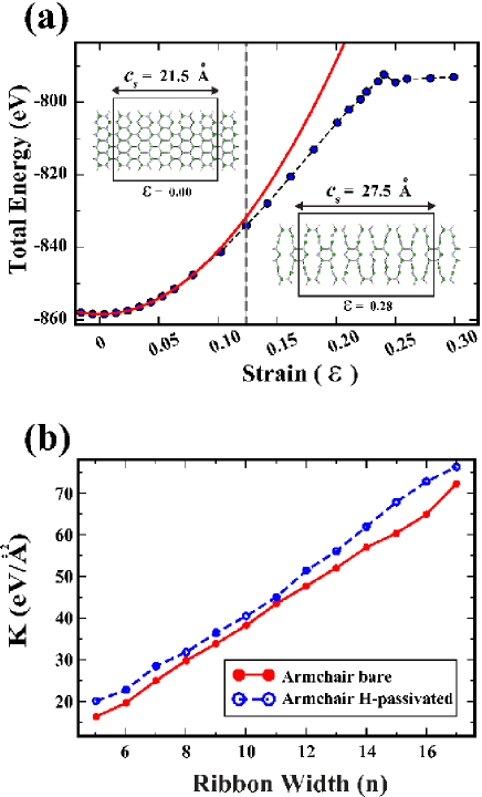
In Fig. 7 (b) versus the width of the ribbon in terms of the number of B-N pair in the primitive unit cell is plotted for bare and hydrogen passivated A-BNNR. shows an approximately linear variation indicating that the force constant is directly proportional to the width of the ribbon. One also sees that the strength of the ribbon increases upon passivation with hydrogen.
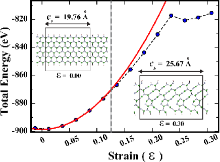
The behavior of bare and hydrogen passivated Z-BNNR under uniaxial tensile stress is similar to that of A-BNNR. In Fig. 8 three regions, namely elastic harmonic, elastic-anharmonic and plastic regions are seen. The sudden change in the curve at indicates a structural phase transformation, where the lattice constant elongates from the initial value of 19.8 Å to 25.7 Å corresponding to . The structure of hydrogen passivated Z-BNNR before and after the structural transformation are shown as inset. Variation of versus the ribbon width is calculated for bare and hydrogen passivated Z-BNNR show an overall linear behavior as presented in Fig. 7 (b).
V.3 Vacancy and antisite defects
It is known that the vacancy defect in 2D graphene esquinazi ; Iijima ; yazyev ; guinea ; brey2 and graphene nanoribbons brey1 ; delik give rise to crucial changes in the electronic and magnetic structure. According to Lieb’s theorem lieb , the net magnetic moment per cell is determined with the difference in the number of atoms belonging to different sublattices, i.e. . While DFT calculations on vacancies in 2D graphene and armchair graphene nanoribbons confirmed Lieb’s theorem, results are diversified for vacancies in zigzag graphene nanoribbons brey1 ; delik . Therefore, the effect of vacancy defects on the properties of BNNRs is of interest.
Earlier activation energies and reaction paths for diffusion and nucleation mono and divacancy in h-BN layers have been investigated by using density functional tight-binding method zobelli . The formation energies were calculated to be 11.22 eV and 8.91 eV, for a B- and N-vacancy, respectively. The possible magnetism induced by nonmagnetic impurities and vacancy defects in a BN sheet have been investigated from the first-principles. The magnetic moment associated by nonmagnetic atoms substituting B or N has been calculated to be liu . Based on first-principles calculations, the magnetic moment of a N-vacancy in a 2D BN sheet has been predicted to be 1 . In the case of a B-vacancy, three neighboring N atoms are displaced further apart from each other and the net magnetic moment is predicted to be 3 si . Another calculation of defects in a BN monolayer found that three dangling bonds associated with a B-vacancy lead to total spin S=3/2, i.e 3 azeveda .
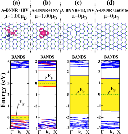
The effects of vacancies of BN nanoribbons have not been treated yet. Here we investigated the effect of B-, N-, B+N-divacancy and B+N-anti site on the electronic and magnetic properties of A- and Z-BNNR. Within periodic boundary conditions, a vacancy defect in an A-BNNR of width is repeated in every 5th primitive unit cell to yield minute defect-defect coupling. As shown in Fig. 9 (a) A-BNNR with B-vacancy becomes ferromagnetic with a net magnetic moment of per unit cell. Similarly, a N vacancy gives rise to a net magnetic moment of per unit cell. A-BNNR having either periodic B+N-divacancy or anti site defect for every five unit cell remain nonmagnetic. The calculated values of magnetic moments are in compliance with Lieb’s theorem. We found that the structural relaxation is crucial to obtain correct values of magnetic moments. In particular, initially we calculated for relaxed structure of the B-vacancy. However, the neighboring N atoms distorted slightly from their equilibrium, the structure is relaxed further and had lowered the total energy. As a result, the magnetic moment was calculated as . The energy band structures in Fig. 9 (a)-(d) are calculated for periodic vacancy defects repeating in every four primitive cell. The Fermi levels are assigned according to the occupancy of vacancy states. We note that the empty state associated with the B-vacancy in Fig. 9 is hole like. The states associated with the N-vacancy occur near the edge of the conduction band are donor like.
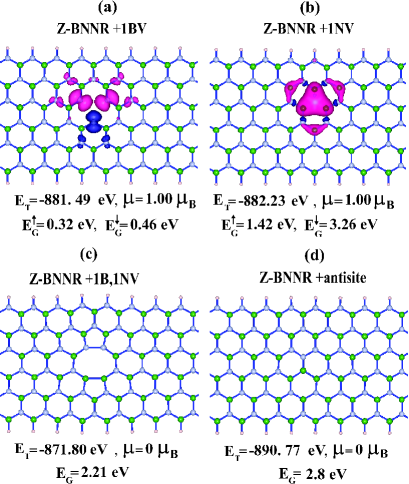
The situation with Z-BNNR is similar to that in A-BNNR discussed above, since hydrogen passivated Z-BNNR is nonmagnetic as A-BNNR. A periodic B- or N-vacancy repeated in every eight unit cell of hydrogen saturated Z-BNNR with =6 has a net magnetic moment of per supercell. Whereas Z-BNNR passivated with hydrogen atoms at both edges and having either periodic B+N-divacancy or anti site defect repeating in every eight unit cell is nonmagnetic. The type of the periodic vacancy defect modifies the band gap of Z-BNNR from 4.2 eV to 2.21 eV for divacancy, but to 2.8 eV for anti site. The calculated magnetic moment of hydrogen passivated Z-BNNR are in agreement with Lieb’s theorem. We note that in zigzag graphene nanoribbons magnetic edge states survive even after hydrogen passivation, and interact with the magnetic moments of vacancies delik . This interaction causes deviation from the prediction of Lieb’s theorem.
VI Discussion and Conclusions
In various allotropic forms of BN the dimensionality play a crucial role. For the sake of comparison, we present the calculated values of BN for different allotropic forms of BN in different dimensionalities. One sees that the B-N double bond of 1D BN atomic chain is shortest and is 1.31 Å. The s bond of h-BN and 2D BN has intermediate value of 1.45 Å. Therefore, h-BN can considered to be quasi two dimensional. Three dimensional wurtzite and zincblende BN crystal have s-bonding with Å, which is largest among the allotropic forms studied here. According to GGA results the cohesive energy of 2D BN is 3 meV larger than that of h-BN. This is due to fact that the GGA calculation cannot account the van der Waals interaction between atomic layers of h-BN. However, the calculations using LDA, where the van der Waals interactions are better accounted, yield the cohesive energy of h-BN is 57 meV larger than that of 2D BN as one expects. The charge transfer from B to N atom increases with decreasing dimensionality. This due to fact that decreases with decreasing dimensionality. As for the coordination number increases with increasing dimension.
In 2D BN honeycomb structures and in its zigzag and armchair nanoribbons, the B-N bond formed from the bonding s hybrid orbitals from B and N atoms is essential. Owing to the transfer of charge from B to N the B-N bond acquires an ionic character, which underlies the semiconducting properties with wide band gap.
| EG | Q | Lattice | |||
|---|---|---|---|---|---|
| 1D Chain | 1.307 | -16.04 | 3.99 | 0.511 | a=2.614 |
| 2D BN | 1.452 | -17.65 | 4.64 | 0.429 | a=2.511 |
| h-BN | 1.450 | -17.65 | 4.47 | 0.416 | a=2.511 , c/a=2.66 |
| Wurtzite | 1.561 | -17.45 | 5.726 | 0.342 | a=2.542 , c/a=1.63 |
| Zincblende | 1.568 | -17.49 | 4.50 | 0.334 | a=2.561 |
Bare armchair nanoribbon of 2D BN is again a nonmagnetic wide band gap semiconductor, the band gap of which is practically unaltered with width . Upon passivation with hydrogen band gap of the ribbon increase by 0.3 eV. As for zigzag nanoribbons, they provide a number of interesting properties. When its both edges are bare, it is ferromagnetic metal. When its N-edge is passivated with hydrogen, it becomes an antiferromagnetic semiconductor. In the reverse case, namely when B-side is passivated, it becomes a ferromagnetic semiconductor. When both edges are passivated, it becomes a nonmagnetic, wide band gap semiconductor. The band gap as well as the magnetic state of a ribbon can be modified by periodic vacancy defects. Finally, BN nanoribbons have been found to be strong, quasi one dimensional and stable structures. They can sustain up to high strains, and they stretch in the plastic region with structural transformations.
Briefly, the calculated electronic, magnetic and mechanical properties of 2D BN honeycomb structure and its nanoribbons present interesting but some differences from graphene. In this respect BN honeycomb structure and its nanoribbons are complimentary to graphene. The properties of 2D BN honeycomb structure can be changed upon functionalization with foreign atoms. Interesting quantum structures (such as single and series quantum dots, resonant tunneling double barriers and multiple quantum well structures) based on heterostructures and core shell structures of lattice matched graphene and BN can be formed, since the band gap of BN is much larger than that of graphene.
Acknowledgements.
Part of the computational resources have been provided by UYBHM at Istanbul Technical University through grant Grant No. 2-024-2007. E. Aktürk gratefully acknowledgments the receipt of a BIDEB Postdoctoral Fellowship from TUBITAK.References
- (1) K. S. Novoselov, A. K. Geim, S. V. Morozov, D. Jiang, Y. Zhang, S. V. Dubonos, I. V. Grigorieva, A. A. Firsov, Science 306, 666 (2004).
- (2) Y. Zhang, Y.-W. Tan, H. L. Stormer, P. Kim, Nature 438, 201 (2005).
- (3) C. Berger, Z. Song, X. Li, X. Wu, N. Brown, C. Naud, D. Mayou, T. Li, J. Hass, A. N. Marchenkov, E. H. Conrad, P. N. First, W. A. de Heer, Science 312, 1191 (2006).
- (4) A. K. Geim, K. S. Novoselov, Nature Materials 6, 183 (2007).
- (5) Y.-W. Son, M.L. Cohen and S.G. Louie, Nature 444, (2006).
- (6) H. Sevinçli, M. Topsakal, E. Durgun, S. Ciraci, Phys. Rev. B 77, 195434 (2008).
- (7) M. Topsakal; H. Sevinçli, S. Ciraci, Appl. Phys. Lett. 92, 173118 (2008).
- (8) K. S. Novoselov, D. Jiang, F. Schedin, T. Booth , V. V. Khotkevich, S. Morozov, A. K. Geim, Proc. Natl. Acad. Sci. U.S.A. 102, 10451 (2005)
- (9) D. Pacilé, J. C. Meyer, Ç. Ö. Girit, and A. Zettl, Appl. Phys. Lett. 92, 133107 (2008).
- (10) A. Nagashima, N. Tejima, Y. Gamou, T. Kawai, and C. Oshima, Phys. Rev. Lett. 75, 3918 (1995).
- (11) L. Bourgeois, Y. Bando, W. Q. Han, and T. Sato, Phys. Rev. B 61, 7686 (2000)
- (12) N. G. Chopra, R. J. Luyken, K. Cherrey, V. H. Crespi, M. L. Cohen, S. G. Louie, A. Zettl, Science 1995, 269, 966.
- (13) C. Zhi, Y. Bando, C. Tang, and D. Golberg, Appl. Phys. Lett. 87, 063107 (2005).
- (14) D. Golberg, A. Rode, Y. Bando, M. Mitome, E. Gamaly, and B. Luther-Davies, Diamond Relat. Mater. 12, 1269 (2003).
- (15) Y. J. Chen , H. Z. Zhang, Y. Chen, Nanotechnology 17, 786 (2006).
- (16) Z. Zhang and W. Guo, Phys. Rev. B 77, 075403 (2008).
- (17) Cheol-Hwan Park and Steven G. Louie, Nano Lett. 8, 2200 (2008).
- (18) V. Barone, J. E. Peralta, Nano Lett., 8, 2210 (2008)
- (19) X. Li, L. Zhang, S. Lee, H. Dai, Science 319, 1229 (2008).
- (20) X. Wang, Y. Ouyang, X. Li, H. Wang, J. Guo, H. Dai, Phys. Rev. Lett. 100, 206803 (2008).
- (21) P. E. Blöchl, Phys. Rev. B 50, 17953 (1994).
- (22) J. P. Perdew, J. A. Chevary, S. H. Vosko, K. A. Jackson, M. R. Pederson, D. J. Singh, C. Fiolhais, Phys. Rev. B 46, 6671 (1992).
- (23) G. Kresse, J. Hafner, Phys. Rev. B 47, 558 (1993).
- (24) G. Kresse, J. Furthmüller, Phys. Rev. B 54, 11169 (1996).
- (25) S. Baroni, A. Del Corso, S. Girancoli and P. Giannozzi, http:/www.pwscf.org/
- (26) A. Catellani, M. Posternak, A. Baldereschi, A. J. Freeman, Phys. Rev. B 36, 6105 (1987).
- (27) L. Liu, Y. P. Feng, and Z. X. Shen, Phys. Rev. B 68, 104102 (2003).
- (28) N. Ooi, V. Rajan, J. Gottlieb, Y. Catherine, and J. B. Adams, Modell. Simul. Mater. Sci. Eng. 14, 515 (2006).
- (29) K. Shimada, T. Sota, and K. Suzuki, J. Apl. Phys. 84, 9 (1998).
- (30) M. P. Surh, S. G. Louie, and M. L. Cohen, Phys. Rev. B 43, 9126 (1991).
- (31) R.T. Senger, S. Tongay, E. Durgun and S. Ciraci, Phys. Rev. B 72, 075419 (2005).
- (32) A.V. Kurdyumov, V.L. Solozhenko, and W.B. Zelyavski, J. Appl. Crystallogr. 28, 540 (1995).
- (33) Caution has to be taken in using the values of band gap calculated with DFT as in the present study, since the value of band gap is usually underestimated by DFT.
- (34) The calculations of have been carried out by using PWSCF software pwscf .
- (35) S. Tongay, R.T. Senger, S. Dag and S. Ciraci, Phys. Rev. Lett. 93, 136404 (2004).
- (36) E. Rokuta, Y. Hasegawa, K. Suzuki, Y. Gamou, C. Oshima and A. Nagashima, Phys. Rev. Lett. 79, 4609 (1997).
- (37) L. Wirtz, A.Rubio, R.A. delaConcha, A. Loiseau, Phys. Rev. B 68,045425 (2003).
- (38) G. Kern, G. Kresse and J. Hafner, Phys. Rev. B 59, 8551 (1999).
- (39) W.J. Yu, W.M. Lau, S.P.Chan, Z.F. Liu, Q.Q. Zheng, Phys. Rev. B 67, 014108 (2003).
- (40) J. Serrano, A. Bosak, R. Arenal, M. Krisch, K. Watanabe, T. Taniguchi, H. Kanda, A. Rubio, and L. Wirtz, Phys. Rev. Lett. 98, 095503 (2007).
- (41) V. L. Solozhenkan, G. Will and F. Elf, Solid State Commun. 96,1 (1995).
- (42) Y. Miyamoto, M. L. Cohen, and S. G. Louie, Phys. Rev. B 52, 14971 (1995).
- (43) F. Liu, P. Ming and J. Li, Phys. Rev. 76, 064120 (2007).
- (44) D. Alfè, http://chianti.geol.ucl.ac.uk/ dario.
- (45) V. Barone, O. Hod and G.E. Scuseria, Nano Lett. 6, 2748 (2006).
- (46) P. Esquinazi , D. Spemann, R. Höhne, A. Setzer, K.-H. Han, T. Butz, Phys. Rev. Lett. 91, 227201 (2003).
- (47) A. Hashimoto,K. Suenaga, A. Gloter, K. Urita, S. Iijima, Nature 430, 870 (2004).
- (48) O. V. Yazyev and L. Helm, Phys. Rev. B 75, 125408 (2007).
- (49) M.A.H. Vozmediano, M.P. Lopez-Sancho, T. Stauber and F. Guinea, Phys. Rev. B, 72, 155121 (2005).
- (50) L. Brey, H.A. Fertig, and S. Das Sarma, Phys. Rev. Lett. 99, 116802 (2007).
- (51) J.J. Palacios, J. Fernandez-Rossier, and L. Brey, Phys. Rev. B. 77, 195428 (2008).
- (52) M. Topsakal, E. Aktürk and S. Ciraci. Phys. Rev. B 78,xxxxx (2008).
- (53) E.H. Lieb, Phys. Rev. Lett. 62, 1201 (1989).
- (54) A. Zobelli, C.P. Ewels, A.Gloter and G. Seifert, Phys. Rev. B 75, 094104 (2007).
- (55) R.F. Liu and C. Cheng, Phys. Rev. B 76, 014405 (2007).
- (56) M.S. Si and D.S. Xue, Phys. Rev. B 75, 193409 (2007).
- (57) S. Azeveda, J.R. Kashny, C.M.C. de Castilhoand F. De Brito, Nanotechnology 18, 495707 (2007).