First-Principles conductance of nanoscale junctions from the polarizability of finite systems
Abstract
A method for the calculation of the conductance of nanoscale electrical junctions is extended to ab-initio electronic structure methods which make use of the periodic supercell technique, and applied to realistic models of metallic wires and break-junctions of sodium and gold. The method is systematically controllable and convergeable, and can be straightforwardly extended to include more complex processes and interactions. Important issues about the order in which are taken both the thermodynamic and the static (small field) limits are clarified, and characterized further through comparisons to model systems.
I Introduction
Nanoscale and molecular electronics is one of the most active topics of research in physics todayvenkataraman_2006_conductance_exp_conformation ; Quek07 ; venema_2008_organic_electronics ; it has very important consequences, both for fundamental research and for industrial processes, which will reach their inherent quantum limits in the decade to come. Accurate methods of theoretical as well as experimental characterization are essential, and many open questions remain about the structure, equilibrium, and dynamics of nanometer-sized systems carrying electrical currents. The ab initiosimulation of materials properties is in a unique position to develop the scope and our understanding of electronics at the nanoscale, providing the only method of systematic analysis of electronic and structural effects, which are never all simultaneously accessible in experiment. Present simulations of nanoscale transport usually fall into two categories, either employing time-dependent density functional theory (TDDFT)kurth_2005_tddft_transport ; Bushong05 ; Qian06 or various flavors of Landauer-Büttiker-like formulasDiVentra00 ; Evers04 ; Koentopp08 , sometimes using a non-equilibrium Green’s function formalismkeldysh_1965_negf (for a review see Ref. Koentopp08, ). Due to the way they are formulated, using embedding schemes, these techniques often rely on localized functions (atomicBrandbyge02 ; Evers04 ; Toher05 ; Choi07 ; beste_2008_basis_set_effect_transport or WannierCalzolari04 ; Strange08 functions) to describe the single particle wavefunctions of the system. This introduces an inherent difficulty in converging calculations, as the basis sets usually cannot be refined systematically. There is still a great deal of uncertainty about the precision of both experiments, e.g. due to fluctuation in experimental conditions of contact and current flow, and theory, where no standard model is yet accepted as being predictive of experiments, apart from simple cases of continuous contact with conductances of at least one quantum of conductance (). The role and importance of electron-electronDelaney04 ; Ferretti05 ; Cehovin08 ; Thygesen08 ; Myohanen08 ; Koentopp08 and electron-vibrationVerdozzi06 ; Frederiksen07 ; Galperin08 interactions, has been recognized as an important factor in obtaining the correct transport properties even though satisfactory treatment for a general system at the ab initio level is not yet available.
In the following, we present a method to calculate the conductance of a quantum junction, which can be systematically converged and extended to include the effects of different interactions. The formalism has been previously applied to model systems in 1Dbokes_2004_conductance and jellium slabsbokes_2007_four_point_conductance , and is here extended to incorporate 3D realistic ab initio electronic structures at the level of local or semi-local time-dependent density-functional theory. Section II describes the method and how it must be adapted to suit the periodic boundary conditions and supercells which are often used in ab initio calculations. Preliminary numerical characterization is carried out in Section III. Section IV analyzes the convergence properties of the method and applies it to monatomic wires of sodium. In particular, the possibility of obtaining precise calculations of very low conductances is explored for a tunnel junction. Finally, Section V examines contact geometry and bonding effects for bulk gold electrodes.
II Methodology
The conductance of a nanojunction characterizes the long-time dynamics of the electronic response of electrons to a driving electric field bokes_2007_four_point_conductance . While formally the long-time limit demands the study of an extended system, for calculation purposes it is possible to consider a finite model for a finite time and the resulting conductance is obtained by extrapolation of the conductance function
| (1) |
where is the two-point conductance (see Ref. bokes_2007_four_point_conductance ). The order of limits is important here: the one given characterizes transport in an extended system where as the reverse would reflect damped oscillations of density in a finite (even though large) system. The underlying finite system can fulfill any boundary conditions and these do not affect the extrapolated results. We take advantage of this fact and use the periodic boundary conditions and a plane-wave basis for the ab initio calculations below.
It is presumed in the following that the junction whose conductance we are searching for is centered at 0 in the middle of the cell (which thus extends from to ).
The calculation of the electronic response function at the level of local or semi-local TD DFT, which then leads to the conduction function (Eq. 1), proceeds in three steps. First we perform a calculation of the occupied () as well as the unoccupied () eigenenergies and eigenstates of the system.
Second, we use the eigenvalues and eigenstates to compose the positive imaginary-time Matsubara Green’s function
| (2) |
As is anti-periodic in imaginary time (fermionic) there is no need to specify explicitly its behavior for negative imaginary time.
The electronic response to the total electric field is characterized by the polarizability
| (3) | |||||
which, after Fourier transformation, , and integration over the cross-sectional area of the junction, , gives the integrated polarizability relevant for charge transport
| (4) |
Methods going beyond the present level of approximations, i.e. using nonlocal exchange-correlation kernelsSai05 ; Jung07 or Green’s-function-based many-body methodsOnida02 , would differ in the above Equations 2 and 3. The expression for the irreducible polarizability, Eq. 3, would contain further vertex diagramsOnida02 and, in the case of many-body methods, the Green’s function cannot be expressed in terms of one-electron wavefunctions as in Eq. 2. However, the discussion that follows would apply also to these computationally more demanding approaches.
Finally, the third step consists of integrating the polarizability to obtain the conductance function. For an infinitely long system, the conductance is obtained from the expressionbokes_2007_four_point_conductance
| (5) |
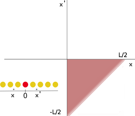
where this integral converges for any finite since for . The integration region corresponds to choosing elements of the polarizability which connect points on opposite sides of the junction. This is intuitive, as we are interested in how a perturbation on one side can influence charges on the other side, through the junction.
For a finite system of length we obtain the corresponding function
| (6) |
where is a domain of positive and negative which must guarantee the correct limiting procedure. Using a periodic supercell, for , we approach a periodic image of the system we want to study. Further, if the system is not translationally invariant we will approach a region of the plane (the lower right hand corner of Fig. 1) where the polarizability behaves very differently from that near (typically one with a more metallic behavior and larger polarizability than the junction). Hence, a correct integration needs to truncate the quadrant defined by and . For a finite system there is no unique choice of , but there is a natural one, which is and , or equivalently , defining a triangle between 0 and the points and (Fig. 1).
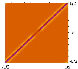
The finite size of the system determines the minimal frequency which can be reliably described in the conductance, or equivalently the longest time propagation. For longer times or lower frequencies the electrons will reach the limits of the system, and the conductance decays. The minimum frequency may be estimated as:
| (7) |
where is the Fermi speed. Thus, an electron at the Fermi level takes time to traverse the whole system. This frequency will be essential in determining how to extrapolate the conductance function to zero frequency.
We apply the formalism described above to systems described by modern electronic structure methods. Many of these techniques use periodic boundary conditions to describe crystalline structures, and represent wavefunctions and electronic densities using plane wave basis sets. Here we describe the corresponding small changes needed in the formalism.
First, as we wish to describe an isolated nanojunction between two leads (which are in principle infinite) we will use only the zone-center k-point of the Brillouin zone (BZ) along the axis of conduction. Using several k-points would in effect simulate an array of interfering junctions. The periodic boundary conditions are nevertheless exploited as the regions near the edge of the simulation cell are described continuously instead of being brutally cut off or terminated with hydrogen atoms. The thermodynamic limit along the conduction axis must still be ensured by increasing the longitudinal system size until the conductance converges.
In the directions perpendicular to a denser k-point grid can be used if bulk three-dimensional leads are considered: the electronic structure of the leads will thus be represented correctly, but care must be taken that the transverse distance between images of the “junction” part of the cell is sufficient to avoid interference between periodic images. In the case of a purely 1D system no perpendicular k-points are necessary as the system is supposed to be isolated in vacuum along and .
III Numerical characterization
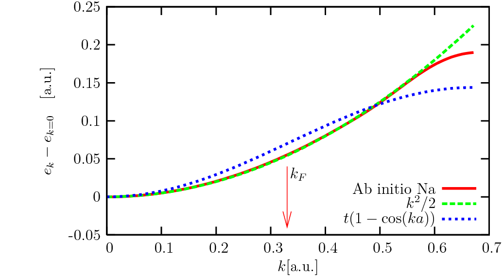
In order to understand the convergence behavior of the main results we have also analyzed a finite 1D jellium model and a finite 1D tight-binding model. The length of both systems can be made much larger than in the ab initio models, which allows detailed study of the extrapolation to small frequencies. Similarly to the ab initio case, both models use periodic boundary conditions and their parameters are such that the density and the Fermi speed of the particles will be identical to that of a sodium chain studied within the self-consistent ab initio calculations. In fact, the jellium model with a bare electron mass is an excellent model for the sodium wires. This is shown in the Fig. 2 where the dispersion of eigenenergies, obtained from the ab initio calculations, is compared with the dispersion of the 1D jellium and the fitted TB model. More generally, these two models represent two extremal types of electronic structure for metallic wires. The correct understanding of the extrapolations to infinite size and zero frequency of their conductance functions is very useful for performing extrapolations of more realistic but numerically more demanding ab initio calculations.
For both model systems one can find the eigenstates exactly by going into reciprocal space. The conductance function (Eq. 6) can be expressed using the exact eigenstates of the Hamiltonian
| (8) |
where the sum goes over all eigenstates, or are the momenta of the eigenstates, are Fermi occupancies of the state at temperature , are the eigenenergies corresponding to an eigenstate with the momentum , and the factor 2 accounts for the spin degeneracy. The function represents the conductance vertex-factor (similarly to the expression for the conductivity in terms of the polarization function, see e.g. Bruus and Flensbergbruus_2004_many_body_book ) and takes different forms for the two systems, as given below.
The jellium model consists of a 1D non-interacting electron gas of total length and density where is the total number of electrons. The eigenvalues are
| (9) |
and the conductance vertex-factor is
| (10) |
The Fermi energy is obtained from the requirement that the charge per unit length is identical to that of the sodium wires; the length is set to , where is the inter-atomic distance of the sodium wire so that the density of electrons is .
In the case of the tight-binding model, the Hamiltonian has the form
| (11) |
with the resulting eigenvalues for a state with momentum . The momentum only takes discrete values
| (12) |
and the conductance vertex-factor is
| (13) |
At half filling, the Fermi momentum and the Fermi speed is . Making use of the Fermi speed of the sodium wires considered in Sec. IV a.u., we identify the TB parameter as .
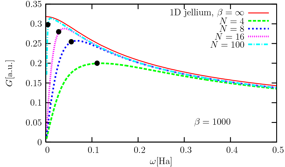
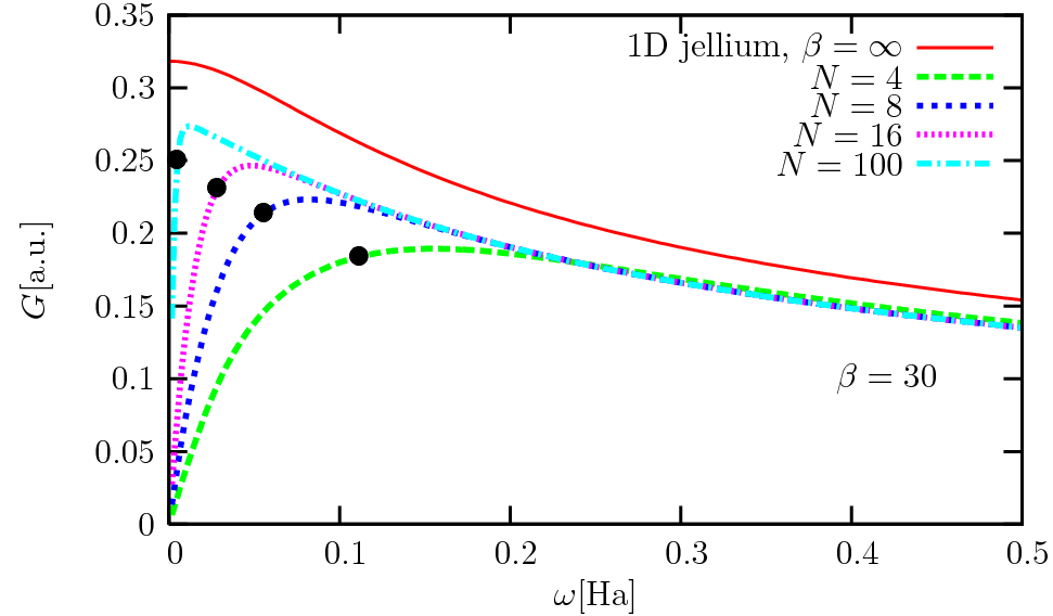
The evaluation of the expression (8) for both models is very fast and can be done for much longer wires than in the case of first-principles calculations. In the top panel of Fig. 3, we show the conductance functions for jellium wires of lengths with and at temperatures much lower than the Fermi energy. The curves converge smoothly to the zero-temperature infinite-length limit that is known analytically bokes_2004_conductance , and readily give the static limit of one quantum of conductance a.u. Furthermore, the functional form shows finite size effects precisely according to the expected criterion (Eq. 7)
| (14) |
for respectively. The extrapolation for or gives good estimates of the conductance, through the limit in Eq. (6). At temperatures comparable with the Fermi energy (bottom graph in Fig. 3) the extrapolated value is somewhat below the zero temperature limit but the functional form of the conductance is essentially identical.
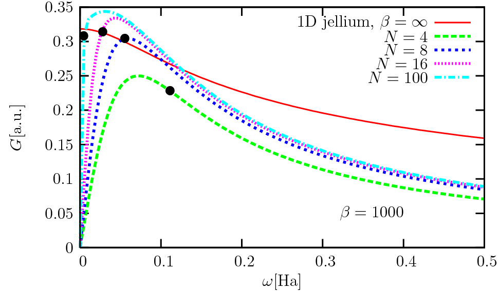
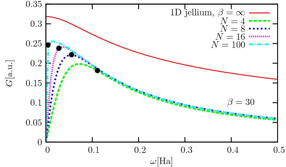
On the other hand, the tight-binding model, shown in the Fig. 4, offers less reliable extrapolations. This is caused by the non-monotonic behavior of the conductance function at small frequencies, which in turn arises because of the bandwidth of the model (here the bandwidth is a.u.). This non-monotonic behavior weakens if we look at the conductance curve at higher electronic temperature. This is shown in the lower graph in the Fig (4) for a temperature comparable to the bandwidth. For these temperatures the conductance function can be easily extrapolated to (high-T) conductance values identical to the jellium model (Fig. 3, lower graph). This suggests that, in principle, by performing the calculations at different electronic temperatures or smearing, one may enhance the extrapolation procedure in realistic calculations, which may combine aspects of free-electron (jellium) and localized electron (TB) behaviors.
To summarize, the models show good convergence in the extrapolated conductance at for systems of length equivalent to 8 or 16 atoms. The jellium dispersion is quite close to the ab initio one for Na, whereas the tight binding one is not - this could be expected from the simple metal nature of sodium. The conductance function of the TB chain is qualitatively different, and actually overshoots the quantum of conductance for small imaginary frequencies and large . Finally, for high temperature (T comparable to ) both models depart from the analytic curves for T=0 and the conductance decreases.
IV Sodium monowires: size convergence and energy dependencies
We begin the ab initio studies with a prototypical application: the calculation of the conductance of a uniform monatomic wire (monowire) of sodium atoms. With one s electron per atom, and given the simple-metal nature of sodium, the conductance in the independent particle case will be two quanta of conductance, due to spin-degeneracy.
Technical details
The ground state wavefunctions and electronic structure are calculated within
density functional theory (DFT)hohenberg_1964_DFT ; kohn_1965_DFT_LDA ,
using a plane wave representation, with the ABINITABINIT_short or
SFHINGXboeck_sfhingx codes (the results have been checked to be
independent of the ground state code used). We employ norm-conserving
Troullier-Martinstroullier_1991_nc_psp type pseudopotentials, with
nonlinear core correctionslouie_1982_NLCC and the d channel as a local
potential. The kinetic energy cutoff (20 Hartree) and number of bands (100 per
Na atom) were over-converged to allow for full checks of the convergence of the
conductance calculation. The calculation of the conductance, in a module of the
GWST coderojas_1995_GWST_prl , was carried out with a kinetic energy
cutoff of 8 Ha.
The inter-atomic distance was set to 2.477 Å. Other distances were checked, but do not influence the results appreciably: the Fermi point for the wire is fixed by the parabolic nature of the bands, and, most importantly in our case, the Fermi speed scales as the inter-atomic spacing, making the critical minimum frequency (Eq. 7) independent of the spacing.
The perpendicular size of the unit cell is more important, as we wish to simulate a truly 1D system using a supercell. The lateral dimensions of the unit cell are fixed to 4 Å, which is enough to ensure that conductance only happens along the wire direction. Checks with 8 and 16 Å cells showed that the conductance function is already well reproduced to within a few percent.
Results for uniform Na monowires
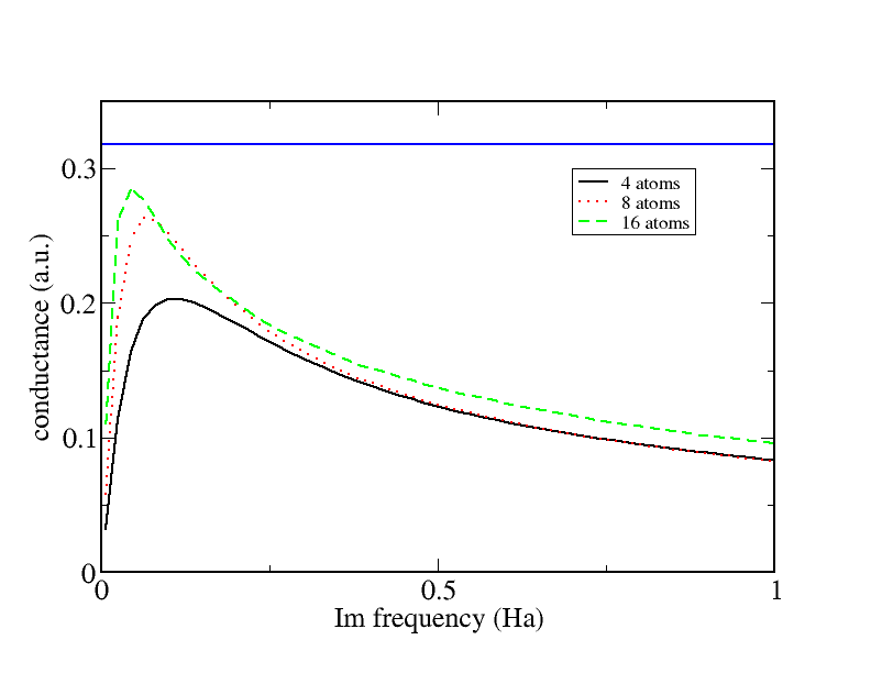
Figure 5 shows the size convergence of the conductance
function, for unit cells containing 4, 8, and 16 atoms. As can be seen in this
simple case the conductance function is correct to lower and lower frequencies
as the system size is increased, and the extrapolation tends towards .
Already with an 8 atom cell the
linear extrapolation of to zero frequency gives a value very close
to , as expected from the previous section.
Comparing the values obtained for successively larger system sizes
gives an estimate of the residual error in converging . A 16 atom unit cell
is about 40 Å long. The very slow convergence of
as a function of is due to the 1D
character of the system. Coulomb screening in 1 dimension is quite inefficient
and the polarizability decays quite slowly. In 3D systems the screening will
be stronger and the size convergence quicker
A very important point is to have a good estimate of the Fermi level. In 1D atomic chains this is not trivial, as the equivalent of k-point sampling is the length of the system. The distance between the levels bracketing the decreases with , but not uniformly. For small , there is an alternation in the position of the Fermi level: for wire lengths which are multiples of 4 the Fermi level is exactly on a single particle state, whereas for other values it is higher, and between states. The dielectric response of these two cases is very different, as one case appears to be a metal and the other an insulator (whose gap goes to 0 as ). In the interest of brevity we have not included the results for with in Fig. 5: they oscillate slightly (as a function of ) and converge more slowly, though to the same end result. We will see these effects again in the next Section for the case of a wire with a gap.
In our formulation the conductance is expressed in imaginary frequency. This implies contributions from all electron hole pairs in the polarizability, not just those for states near the . Because of this the convergence in the number of states is comparable to (but slightly faster than) that of a GW calculation, with between 5 and 20 bands per electron (for Na wires we need 10 bands per electron).
Na monowires with a gap
We now proceed with an inhomogeneous case: a wire of Na atoms with a gap (of
width d). This is the simplest example of a nanojunction. The conductance will
naturally go into a tunneling regime as the gap becomes wider. This example is
important firstly because it has a simple dielectric response,
but also because tunneling is an important and extreme
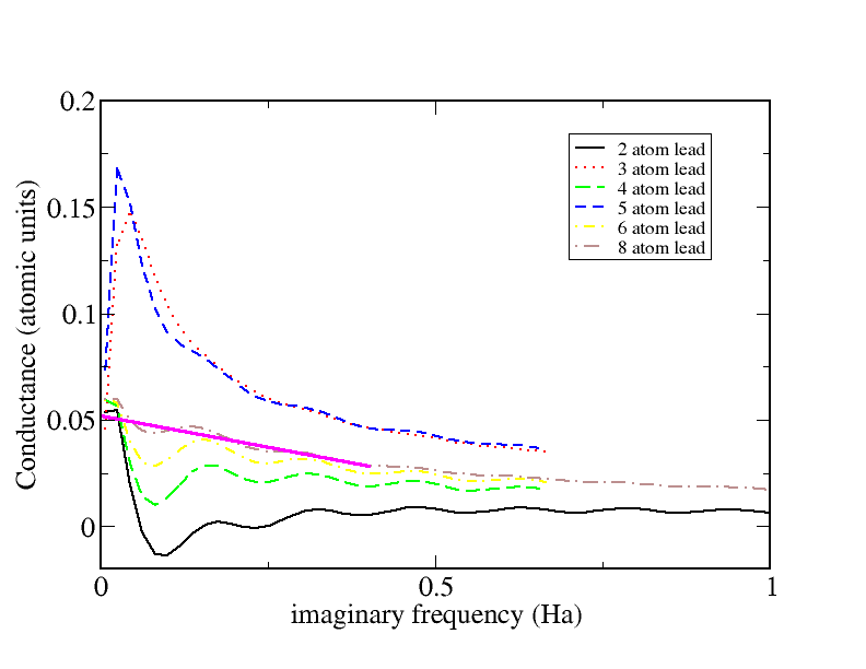
regime for the conductance. Fig. 6 shows the size
convergence of a wire with a gap of one atom. The two remaining parts of the
wire are of equal length, increasing from 2 to 8 atoms (each).
The even length leads converge relatively quickly to a regular conductance
function, from below. The odd length leads converge from above but very slowly,
because the HOMO/LUMO states are quite far apart, which gives a badly placed
Fermi level, as above for continuous wires (bad in the sense that it is far
from the limiting Fermi level for an infinite system). Extrapolation to 0
frequency gives a conductance of 0.05 a.u. ().
The oscillations of are due to aliasing effects in the Fourier transform from imaginary time to imaginary frequency. These are in some cases difficult to eliminate for very low amplitude elements of .
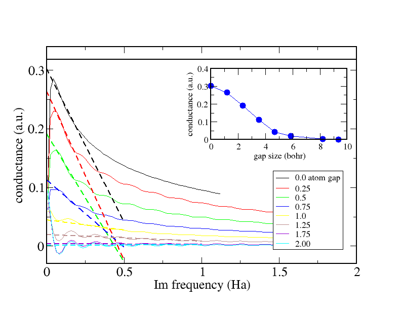
Finally we consider the transition from the conducting to the tunneling regime, by increasing the gap size (for 8 atom leads). The conductance functions are represented in Fig. 7, with the inset showing the decrease of the extrapolated static conductance as a function of the size of the gap. The conductance decreases with gap size, and by a gap of of an atomic spacing (about 4 Bohr) the tunneling regime begins with exponential decay of . The tail of gives a very good fit to where and are in atomic units. The dashed lines are linear extrapolations of fit to the interval Hartree. For the lowest curves (largest gaps) the fit was performed further out, on , as the functions are flatter and the aliasing noise more important. In this way we are able to represent quite small conductance values, down to 0.001 a.u. (or 0.003 ).
A similar system was examined by Beste et al. in Reference beste_2008_basis_set_effect_transport, , but with gold chains instead of Na. They find a conductance of about 0.12 a.u. for a gap of (1.28Å), which is close to our value of 0.18 a.u. for . One important conclusion of Ref. beste_2008_basis_set_effect_transport is the very strong deviations which can appear depending on the basis set nature, with localized basis sets. Our results can be converged systematically, using a plane-wave basis set, but are probably heavier calculations as a trade-off.
V Gold wires: lead structure and k-point sampling
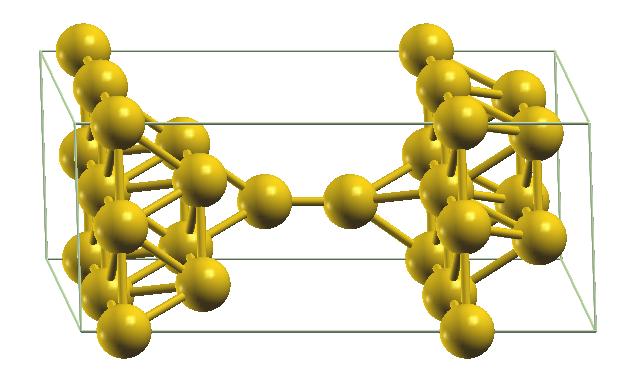
We now proceed with a more structured system, showing an explicit constriction. A gold junction is made from a 2 atom wire contacted to bulk 3D electrodes. The electrodes are FCC stacked gold (at the experimental nearest neighbor distance of 2.9 Å of Ref. maeland_1964_au_acell, ) of which we use a 22 (111) surface unit cell. The wire atoms are evenly spaced with the FCC inter-layer distance of 2.37 Å (which is compressed compared to the DFT-LDA equilibrium distance of 2.5 Å for the infinite straight wiresanchez-portal_1999_stiff_monatomic ). No relaxation of atomic positions with respect to the bulk is taken into account, but the addition of further structural effects is in no way more difficult; contrary to some other approaches to transportbeste_2008_basis_set_effect_transport ; kurth_2005_tddft_transport we are not constrained to specific unit cell lengths or layer spacings. A typical unit cell is shown in Fig. 8, for the minimal electrode thickness of 2 layers (in each electrode). Electrodes 3 and 4 layers thick were also tested. Because of periodicity, and in order to maintain a continuous FCC structure at the cell boundary, the point of contact of the wire to the right electrode alternates between the different possible FCC stacking sites (for 2 and 4 layer electrodes), and an on-top position (for the 3 layer electrodes). We find little effect of contact position on the conductance of the junction (see below) in this continuously metallic, well contacted case.
Technical details
The pseudopotential we use is of the Hartwigsen-Goedecker-Hutter
flavorhartwigsen_1998_psp_hgh , with only the 6s electrons in the
valence. Our choice of pseudopotential is justified by its softness,
by the chemical homogeneity of the system, and our intention to go
beyond LDA and include many-body corrections. We have performed tests on FCC
gold in the GW approximation (which is beyond the scope of the present
article), including the 5d electrons. The problems recognized by Marini et
al.marini_2001_Cu_GW for Cu appear for Au as well: the exchange
self-energy is quite badly represented for the 5d electron states, due to the
absence of the 5s and 5p. The latter are far in energy but have an important
spatial overlap with the 5d. Consequently, the exchange self-energy lacks
important contributions if one uses only the valence electrons. The GW d bands are very
poor (whereas their position in LDA is very close to experimental values);
some bands are pushed down and others up to the Fermi level, which would change
the conductance severely. The use of
a purely 6s potential is less realistic but reduces these exchange effects
(which are now between the 6s and the core 5d states). A more complete solution is
that adopted by Shishkin and Kresseshishkin_2006_GW_PAW in the PAW
formalismblochl_1994_PAW . As PAW allows explicit reconstruction of the
core states, the exchange with the valence can be calculated explicitly.
Finally, the d electrons do not complexify the independent particle conductance
calculation formally, but do make the calculations much heavier (with an
additional 10 electrons per atom). As the states at the Fermi level are purely
s-electron like, the conductance will not be affected strongly. However, as our
method is an integral of the dielectric response of the system, the
absence of the d electrons will have an indirect effect, through
changes in the polarizability.
Results
From a calculation of a uniform wire (with k-points along the wire axis), we
estimate the Fermi speed in the wire to be 0.42 au ( m/s),
corresponding to a wavelength of 7.22 Bohr. A simple metal approximation for
the bulk gives an estimated Fermi speed of 0.64 au ( m/s) from the
Au Seitz radius. A DFT calculation of FCC bulk naturally gives a more complex
band structure - the modulus of the Fermi speed varies by some 20% in
reciprocal space. The HGH pseudopotential gives an average value of 1.02 au
( m/s). A more complete pseudopotential with d electrons reduces
this value to 0.67 au ( m/s). The value we are interested in is
the speed of propagation of an electronic signal through the whole system, i.e.
through the 3D bulk (with the pseudopotential we are using) and the wire, which
will be between the pure bulk and pure wire values.
With the bulk and wire , we can estimate the minimal frequencies which can be represented
for different unit cell sizes. With cells of lengths 27, 36, and 45 Bohr,
we obtain 0.163, 0.132, and 0.113 Hartree.
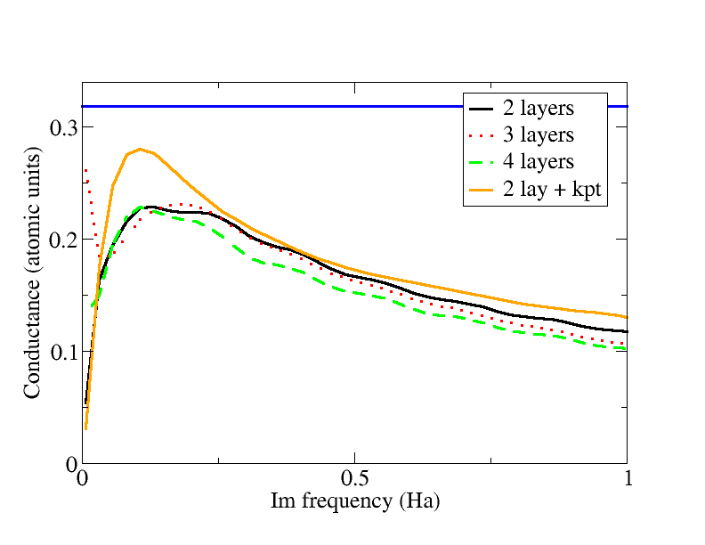
In Fig. 9 (lowest three curves) we represent the conductance as a function of imaginary frequency for a series of gold junctions (like that schematized in Fig. 8) with 2, 3 and 4 layers of FCC gold in the bulk leads. As before for linear wires, initially only the point wavefunctions are used, and takes similar values to the case without leads, which would suggest a similar system length of ca. 8 layers in each lead to converge the conductance. The extrapolated value, close to the quantum of conductance is in agreement with the results of the more extended models of the monatomic gold contacts Jelinek08 .
With bulk leads it is essential to look at k-point convergence: to represent the bulk states correctly, we increase the sampling of k-points in the direction perpendicular to the junction axis. Again, as noted above, one must also take care to keep the nanojunctions themselves well isolated in the perpendicular direction, to avoid interference effects which would be amplified by the perpendicular k-points. With 2 layer leads and a 44 sampling of k-points, we find the conductance function shown by the top curve of Fig. 9. The low frequency behavior is now much closer to that of the longer Na wires. Increasing the lead size thus has two effects, which are controllable separately in this 3D case: first improving the representation of the density of states (DOS) (which can also be achieved by using the perpendicular k-points if the leads are bulk-like), and second lowering the minimum representable frequency (which can only be achieved by increasing the system length L). In the future, a more extended study will combine the effects of longer leads and perpendicular k-point sampling, but the computational load will require the parallelization of our code, which is underway.
To summarize, the bulk leads on gold wires show that even with relatively small system sizes a constriction limits the conductance to a single quantum of conductance. Bulk 3D leads give much stronger screening than 1D ones, and faster convergence of the conductance function. Including k-points to sample the perpendicular electronic states in the leads improves the description of the DOS and the screening.
VI Conclusions
We present a new method to calculate the transport properties of nanoscopic junctions. The extension of the basic formalism to periodic systems and realistic electronic structure is detailed, and the convergence properties are compared to model systems. Order-of-limits problems are reviewed, which also concern many other approaches to quantum transport, as well as numerical issues. The differences and inherent advantages of the method are discussed, in particular the way it treats leads and its systematic convergeability in number of single particle states and the spatial representation of different quantities. Applications to sodium and gold nanojunctions is presented. The first show the properties of purely 1D systems, and demonstrate the variation between regimes of continuous metallicity and of tunnel junctions. The gold junctions explore contact geometries and some of the fundamental differences between 1D and 3D electrode structure and screening.
Acknowledgements.
The authors wish to acknowledge fruitful discussions with A. Ferretti, P. Rinke, and C. Freysoldt. This research has been supported by the NANOQUANTA EU Network of Excellence (NMP4-CT-2004-500198), the NATO Security Through Science Programme (EAP.RIG.981521) and by Marie Curie fellowship MEIF-CT-2005-024152. Some computer time was provided by the White Rose Grid.References
- (1) L. Venkataraman, J. Klare, C. Nuckolls, H. M.S., and M. Steigerwald, Nature 442, 904 (2006).
- (2) S. Y. Quek, L. Venkataraman, H. J. Choi, S. G. Louie, M. S. Hybertsen, and J. B. Neaton, Nano Letters 7, 3477 (2007).
- (3) L. Venema, Nature 453, 996 (2008).
- (4) S. Kurth, G. Stefanucci, C.-O. Almbladh, A. Rubio, and E. Gross, Phys. Rev. B 72, 035308 (2005).
- (5) N. Bushong, N. Sai, and M. D. Ventra, Nano Lett. 5, 2569 (2005).
- (6) X. Qian, J. Li, X. Lin, and S. Yip, Phys. Rev. B 73, 035408 (2006).
- (7) M. D. Ventra, S. T. Pantelides, and N. D. Lang, Phys. Rev. Lett. 84, 979 (2000).
- (8) F. Evers, F. Weigend, and M. Koentopp, Phys. Rev. B 69, 235411 (2004).
- (9) M. Koentopp, C. Chang, K. Burke, and R. Car, J. Phys.: Condens. Matter 20, 083203 (2008).
- (10) L. Keldysh, Sov. Phys. JETP 20, 1018 (1965).
- (11) M. Brandbyge, J. L. Mozos, P. Ordejon, and J. T. K. Stokbro, Phys. Rev. B 65, 165401 (2002).
- (12) C. Toher, A. Filippetti, S. Sanvito, and K. Burke, Phys. Rev. Lett. 95, 146402 (2005).
- (13) S. G. L. Hyoung Joon Choi, Marvin L. Cohen, Phys. Rev. B 76, 155420 (2007).
- (14) A. Beste, V. Meunier, and R. J. Harrison, J. Chem. Phys. 128, 154713 (2008).
- (15) A. Calzolari, N. Marzari, I. Souza, and M. B. Nardelli, Phys. Rev. B 69, 035108 (2004).
- (16) M. Strange, I. S. Kristensen, K. S. Thygesen, and K. W. Jacobsen, J. Chem. Phys. 128, 114714 (2008).
- (17) P. Delaney and J. C. Greer, Phys. Rev. Lett. 93, 036805 (2004).
- (18) A. Ferretti, A. Calzolari, R. D. Felice, F. Manghi, M. J. Caldas, M. B. Nardelli, and E. Molinari, Phys. Rev. Lett. 94, 116802 (2005).
- (19) A. Cehovin, H. Mera, J. H. Jensen, K. Stokbro, and T. B. Pedersen, Phys. Rev. B 77, 195432 (2008).
- (20) K. Thygesen, Phys. Rev. Lett. 100, 166804 (2008).
- (21) P. Myöhänen, A. Stan, G. Stefanucci, and R. van Leeuwen, Europhysics Lett. 84, 67001 (2008).
- (22) C.-O. A. Claudio Verdozzi, Gianluca Stefanucci, Phys. Rev. Lett. 97, 046603 (2006).
- (23) T. Frederiksen, M. Paulsson, M. Brandbyge, and A.-P. Jauho, Phys. Rev. B 75, 205413 (2007).
- (24) M. Galperin, A. Nitzan, and M. A. Ratner, Phys. Rev. B 78, 125320 (2008).
- (25) P. Bokes and R. W. Godby, Phys. Rev. B 69, 245420 (2004).
- (26) P. Bokes, J. Jung, and R. Godby, Phys. Rev. B 76, 125433 (2007).
- (27) N. Sai, M. Zwolak, G. Vignale, and M. D. Ventra, Phys. Rev. Lett. 94, 186810 (2005).
- (28) J. Jung, P. Bokes, and R. W. Godby, Phys. Rev. Lett. 98, 259701 (2007).
- (29) G. Onida, L. Reining, and A. Rubio, Rev. Mod. Phys. 74, 601 (2002).
- (30) H. Bruus and K. Flensberg, Many-body Quantum Theory in Condensed Matter Physics: An Introduction (Oxford University Press, Oxford, 2004).
- (31) P. Hohenberg and W. Kohn, Phys. Rev. 136, 864 (1964).
- (32) W. Kohn and L. J. Sham, Phys. Rev. 140, A 1133 (1965).
- (33) X. Gonze, J.-M. Beuken, R. Caracas, F. Detraux, M. Fuchs, G.-M. Rignanese, L. Sindic, M. Verstraete, G. Zerah, F. Jollet, M. Torrent, A. Roy, M. Mikami, P. Ghosez, J.-Y. Raty, and D. C. Allan, Comp. Mat. Sci. 25, 478 (2002).
- (34) S. Boeck, C. Freysoldt, A. Alsharif, A. Dick, L. Ismer, A. Qteish, and J. Neugebauer, http://www.sfhingx.de .
- (35) N. Troullier and J. L. Martins, Phys. Rev. B 43, 1993 (1991).
- (36) S. G. Louie, S. Froyen, and M. L. Cohen, Phys. Rev. B 26, 1738 (1982).
- (37) H. N. Rojas, R. W. Godby, and R. J. Needs, Phys. Rev. Lett. 74, 1827 (1995).
- (38) A. Maeland and T. Flanagan, Can. J. Phys. 42, 2364 (1964).
- (39) D. Sanchez-Portal, E. Artacho, J. Junquera, P. Ordejon, A. Garcia, and J. Soler, Phys. Rev. Lett. 83, 3884 (1999).
- (40) C. Hartwigsen, S. Goedecker, and J. Hutter, Phys. Rev. B 58, 3641 (1998).
- (41) A. Marini, G. Onida, and R. Del Sole, Phys. Rev. Lett. 88, 016403 (2001).
- (42) M. Shishkin and G. Kresse, Phys. Rev. B 74, 035101 (2006).
- (43) P. E. Blöchl, Phys. Rev. B 50, 17953 (1994).
- (44) P. Jelínek, R. Pérez, J. Ortega, and F. Flores, Phys. Rev. B 77, 115447 (2008).