Electron scattering in intra-nanotube quantum dots
Abstract
Intratube quantum dots showing particle-in-a-box-like states with level spacings up to 200 meV are realized in metallic single-walled carbon nanotubes by means of low dose medium energy Ar+ irradiation. Fourier transform scanning tunneling spectroscopy compared to results of a Fabry-Pérot electron resonator model yields clear signatures for inter- and intra-valley scattering of electrons confined between consecutive irradiation-induced defects (inter-defects distance nm). Effects arising from lifting the degeneracy of the Dirac cones within the first Brillouin zone are also observed.
pacs:
81.07.Ta,73.20.At,68.37.EfThe experimental realization of quantum dots (QDs) QD_Leo , sometimes called “artificial atoms”, has led to a variety of new concepts in nanotechnology underlying advanced QD-based devices for applications in promising fields like nanoelectronics, nanophotonics and quantum information/computation Review_Hanson ; Review_Kern ; Chuang_book . Frequently, for these applications a QD needs to be contacted by source, drain, and gate electrodes. In the field of semiconductor heterostructures the excitation energies of contacted QDs are usually so small that the devices can only be operated at cryogenic temperatures. A promising candidate for room temperature active dots are intra-nanotube QDs formed within a single-walled carbon nanotube (SWNT) by means of two local defects grifoni:2001 . For defect separations of order 10 nm the dot excitation energies are well above 100 meV and thus large compared with at room temperature. Furthermore, the remaining sections of the SWNT to either side of the confining defects provide natural source and drain electrodes. So far, SWNT-based QD prototypes have been realized by tunneling barriers at metal-nanotube interfaces and/or by gate electrodes Review_Christian . Several authors have analyzed defect-induced standing waves by means of scanning tunneling microscopy (STM) Lemay_nat01 ; lieber_PRL ; lee:2004 . However, a detailed description of the scattering dynamics of electrons in and out of the QD is absent. Elaborate studies have only been reported for epitaxial graphene with defects, where an analysis of standing waves in Fourier space has permitted to distinguish between contributions to the wave modulation due to inter- and intra-valley scattering rutter:2007 .

In this Letter we investigate electron standing waves in intra-tube QDs created in SWNTs irradiated with medium energy Ar+ ions. This promising alternative to build intra-tube QDs has been suggested by observations of electronic confinement in metallic SWNTs due to intrinsic defects Bockrath01 . We first show that by virtue of this technique it is indeed possible to realize QDs with a level spacing considerably larger than the thermal broadening at room temperature. Then, by means of Fourier-transform scanning tunneling spectroscopy (FTSTS) combined with a Fabry-Pérot electron resonator model we are able to describe the dominant scattering mechanisms and to identify contributions from inter- and intra-valley scattering.
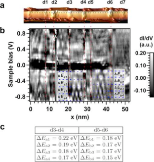
Our measurements were performed in a commercial (Omicron), ultrahigh vacuum LT-STM setup at 5 K. Extremely pure HipCo SWNTs Smalley01 with an intrinsic defect density 0.005 nm-1 were deposited onto Au(111) surfaces from a 1,2-dichloroethane suspension Buchs_NJP_07 . In situ irradiation with medium energy Ar+ ions was performed in a way to achieve a defect density of about 0.1 nm-1 Buchs_Ar . Figure 1a shows a 3D STM image of a nm long portion of an armchair SWNT irradiated with eV ions. Defects induced by medium energy Ar+ ions appear typically as hillocks with an apparent height ranging from 0.5 Å to 4 Å and a lateral extension between 5 Å and 30 Å. We recorded consecutive and equidistant spectra (proportional to the local density of states (LDOS) Tersoff85 ) along the tube axis. Typical data sets, called -scans in the following, consist of 150 spectra recorded on topography line scans of 300 pts. Figure 1b shows a -scan with a spatial resolution 0.34 nm recorded along the horizontal dashed line drawn in (a), running over seven defect sites (d1-d7). A third order polynomial fit has been subtracted from each spectrum to get a better contrast. Defect-induced modifications in the LDOS are revealed as one or more new electronic states at different energy values, spatially localized on the defect sites. First-principle calculations show that medium energy Ar+ ions essentially give rise to single vacancies (SV), double vacancies (DV) and also C adatoms (CAd) on SWNTs Antti_07 . Based on these results we can confidently assume that the created defects in the present work are mainly of vacancy-type.

Several broad discrete states characterized by a modulation of the signal in the spatial direction are observed in the negative bias range between d3-d4 and d5-d6, and in the positive bias range between d2-d3. These states show a discrete number of equidistant maxima following a regular sequence for increasing , similar to the textbook 1D particle-in-a-box model. Within this model it is possible to estimate the level spacing around the charge neutrality point (CNP) for discrete states observed for example in short SWNTs Lemay_nat01 ; Rubio_prl99 . Assuming a linear dispersion around the two inequivalent Fermi points and for a SWNT with finite length , the energy spacing is then given by:
| (1) |
with in nm and the Fermi velocity ms-1 Lemay_nat01 . The energy spacings - in the negative bias range between d3-d4 and - between d5-d6 are reported in Fig. 1c. Using the sequence of maxima we can determine the level spacing closest to the CNP: eV [ eV] between d3-d4 [d5-d6]. This corresponds to a defect distance of nm [ nm] for the defect separation d3-d4 [d5-d6], in good agreement with the measured value at the center of the defect sites nm [ nm] note:one . These results show artificial defect-induced electron confinement regions in metallic SWNTs, i.e. intratube QDs. Importantly, spatially close defects can be generated with our method, allowing level spacings which are much larger than the thermal broadening at room temperature of meV.
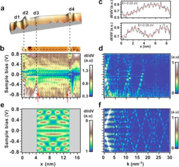
Figure 2a shows a 16 nm long section of a metallic SWNT exposed to 200 eV Ar+ ions with four defect sites (d1-d4). A line-by-line flattened topography image of the same tube between defects d2-d4 is displayed in panel (b) with the corresponding -scan recorded along the horizontal dashed line. Two discrete states are clearly visible in the negative bias range between d3 and d4, at energies eV and eV. The measured energy spacing of about 170 meV fits well with the value of 177 meV obtained from Eq. (1) for a defect separation of about 9.5 nm. Line profiles of signals recorded between the drawn red arrows in (b) and displayed in (c) show a clear oscillatory behavior characterized by a rapid oscillation with an average wavelength of 0.7 nm modulated by a slower variation of the amplitude. This slow modulation, which shows a decreasing wavelength for increasing , has been fitted with the function , where is an arbitrary phase and the factor 2 originates from the fact that is probed.
More details on the observed oscillatory behavior are obtained by means of FTSTS, where line-by-line Fourier transforms are performed on the -scan in Fig. 2b, between the positions indicated by the red arrows. From the resulting map in (d), we observe that the Fourier spectrum of each discrete state is composed of several components note:two . Whereas the individual low frequency peaks between and nm-1 with a high intensity for each discrete state correspond to the slow modulation discussed above, the rapid oscillation in is produced by several components around nm-1 and nm-1. These Fourier components are aligned along sloped lines, indicating the energy dispersive nature of these features. Around nm-1, a unique positively sloped line is clearly visible, with 0.32 eV nm, whereas two lines with positive and negative slopes can be distinguished around nm-1, with a measured slope of about 0.3 eV nm.


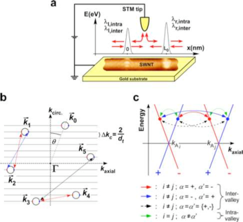
In order to fully explain the experimental features, we use a Fabry-Pérot electron resonator model (see Fig. 3a) considering interference at fixed energy of electron states scattered by impurities. These states can be easily identified considering an unrolled SWNT, i.e. a graphene sheet showing periodic strings of defects along the circumferential direction. The impurities break the translational invariance along the SWNT axis, allowing low energy electron scattering among the six valleys or Dirac cones of the first Brillouin zone. The momenta exchanged in these processes can be decomposed in axial and circumferential components with respect to the tube axis. The former give rise to the interference pattern resulting in the standing waves, whereas the latter modulate the intensity of the standing waves in a non-linear way, i.e. a larger component leads to a lower intensity. In the calculated maps, these standing waves give rise to intensities at -values corresponding to the axial component . Therefore, the maps show a weighted projection of the 2D space of possible scattering vectors along the axial direction. The situation is depicted in Fig. 3b. Two distinct scattering mechanisms take place: intra- and inter-valley scattering. For the first process within the same valley the momentum exchange is small, even zero at the CNP (green process in (c)); the second process connects different valleys (blue, red, and black processes in (b) and (c)). Both scattering mechanisms are related to the presence of SVs and DVs ando05 .
This analysis reduces the scattering processes to a series of weighted 1D scattering events among electrons with a linear energy dispersion and axial momenta (see Fig. 3c). We model the impurities as delta-like potentials placed at a distance , and the STM tip is included by allowing electron tunneling to an external electrode bercioux:2009 ; note:coulomb (see Fig. 3a). Figure 2 shows a comparison between the measured (b) and the calculated (e) LDOS for the case of a SWNT with two identical impurities. The measured SWNT has a chiral angle and shows three dispersion lines at and nm-1, compatible with a metallic SWNT. The numerically evaluated map shown in (f) unveils richer structure than the experimental one. These differences can be attributed to the finite resolution of the tip. The components centered around nm-1 are more intense than the others because they are associated with intra-valley scattering occurring at all six valleys. In the measured the dispersion lines around and nm-1 show a more intense signal for the positive slope branch than for the negative one. For the component centered at 16.8 nm-1, the negative slope branch is almost missing. Similar behavior has been observed in all samples investigated. For armchair SWNTs, this effect has been related to an interplay between symmetry properties of defects and electronic bands resulting in a suppression of scattering lieber_PRL . However, in our case of chiral SWNTs the relation between the parity of the - and -band is more complex and there is no obvious explanation of the observed branch asymmetry. Since our observations are of pivotal importance to the electric transport properties of real SWNT devices, this issue certainly deserve further in depth experimental characterization and theoretical explanation.
If the commensurability condition with integer and the defect separation is not fulfilled, inter-valley scattering takes place only between electrons with opposite direction of motion and implies an asymmetry of the spots in the along the positive and negative slop branches. Contrarily, intra-valley scattering always fulfils this condition with , therefore showing symmetric spots around (see Fig. 3(c)).
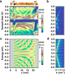
Figure 4a shows a current error image of a metallic SWNT which has been exposed to 1.5 keV Ar+ ions, and the corresponding -scan recorded along the tube axis through two defect sites labeled d1-d2. Here, instead of clear “textbook-like” modes as shown in Fig. 2, we observe curved stripes in the interference pattern between defects d1-d2. However, the corresponding on the right hand side clearly shows well-defined small momentum spots with an average energy separation of about 90 meV in good agreement with Eq. (1) giving meV for a measured defect separation of about 18.5 nm. These features are also captured by the Fabry-Pérot electron resonator model if the two impurities have different scattering strengths , as shown for the simulated -scan with and in Fig. 4b. There is now a clear asymmetry characterized by stripes showing an increasing curvature when moving from the weaker left to the stronger right impurity. There can also be energy dependent differences in the scattering strengths of the defects leading to energy dependent asymmetries in the standing wave pattern as seen in Fig. 1. The choice of ion energy can significantly change the type of defects produced and could therefore potentially be used as a parameter to control to some extend the scattering configuration Buchs_Ar .
In summary, studying intratube QDs in SWNT by FTSTS in combination with simulation, we provided an analysis of the dominant electron scattering processes. Clear signatures for inter- and inta-valley scattering were observed, and scattering effects arising from lifting the degeneracy of the Dirac cones were identified. The here applied strategy will be useful to investigate the scattering properties of other local modifications of SWNTs like e.g. chemical functionalities.
We thank M. Grifoni, O. Johnsen, S. G. Lemay, T. Nakanishi, Y. Nazarov, D. Passerone, C. Pignedoli, and in particular Ch. Schönenberger for fruitful discussions. This work was supported by the Swiss National Center of Competence in Research MANEP, and the Deutsche Forschungsgemeinschaft (DFG).
References
- (1) L. P. Kouwenhoven and C. M. Marcus, Phys. World 11, 35 (1998).
- (2) R. Hanson et al., Rev. Mod. Phys. 79, 1217 (2007).
- (3) J. V. Barth, G. Costantini, and K. Kern, Nature 437, 671 (2005).
- (4) M. Nielsen and I. L. Chuang, Quantum Computation and Quantum Information (Cambridge University Press, Cambridge, UK, 2000).
- (5) H. W. C. Postma et al., Science 293, 76 (2001).
- (6) C. Schönenberger, Semicond. Sci. Technol. 21, S1 (2006).
- (7) S. G. Lemay et al., Nature 412, 617 (2001).
- (8) M. Ouyang, J.-L. Huang and C. M. Lieber, Phys. Rev. Lett. 88, 066804 (2002).
- (9) J. Lee et al., Phys. Rev. Lett. 93, 166403 (2004).
- (10) G. M. Rutter et al., Science 317, 219 (2007).
- (11) M. Bockrath et al., Science 291, 283 (2001).
- (12) I. W. Chiang et al., J. Phys. Chem. B 105, 8297 (2001).
- (13) G. Buchs et al., New J. Phys. 9, 275 (2007).
- (14) A. Tolvanen et al., Phys. Rev. B 79, 125430 (2009).
- (15) I. Horcas et al., Rev. Sci. Instrum. 78, 013705 (2007).
- (16) J. Tersoff and D. R. Hamann, Phys. Rev. B 31, 805 (1985).
- (17) A. Tolvanen et al., Appl. Phys. Lett. 91, 173109 (2007).
- (18) A. Rubio et al., Phys. Rev. Lett. 82, 3520 (1999).
- (19) The slight decrease of for increasing can be attributed to the divergence from linearity of the real dispersion relation for energies far from the CNP ando05 .
- (20) T. Ando, J. Phys. Soc. Jpn. 74, 777 (2005).
- (21) To avoid aliasing effects, we ensure that the highest spectral component fulfills the Nyquist sampling theorem.
- (22) S. Pugnetti et al., Phys. Rev. B 79, 035121 (2009).
- (23) Coulomb interaction in the SWNT is partially screened by the gold substrate and is not taken into account explicitly.