Field-induced Gap and Quantized Charge Pumping in Nano-helix
Abstract
We propose several novel physical phenomena based on nano-scale helical wires. Applying a static electric field transverse to the helical wire induces a metal to insulator transition, with the band gap determined by the applied voltage. Similar idea can be applied to “geometrically” constructing one-dimensional systems with arbitrary external potential. With a quadrupolar electrode configuration, the electric field could rotate in the transverse plane, leading to a quantized dc charge current proportional to the frequency of the rotation. Such a device could be used as a new standard for the high precession measurement of the electric current. The inverse effect implies that passing an electric current through a helical wire in the presence of a transverse static electric field can lead to a mechanical rotation of the helix. This effect can be used to construct nano-scale electro-mechanical motors. Finally, our methodology also enables new ways of controlling and measuring the electronic properties of helical biological molecules such as the DNA.
Helical nanostructures occur ubiquitously in self-assembled form in both inorganic materialsZhang et al. (2002); McIlroy et al. (2001); Zhang et al. (2003); Yang et al. (2004) and in the biological worldXu et al. (2004); Endres et al. (2006). In this paper, we propose several novel physical phenomena based on nano-scale helix wires. Firstly, when a uniform electric field is applied perpendicular to the helical direction, the electrons moving in the nanowire experience a periodical potential due to the potential energy difference. Consequently, such a uniform electric field can induce a gap in the electron energy spectrum, which drives the nanowire from a metallic state to an insulating state if the electron density is commensurate. The general principle behind such a simple phenomenon is that a uniform electric field can generate a nonuniform potential acting on a quantum wire if the quantum wire itself has a curved shape. More generally, one can obtain a quasi one-dimensional system in an arbitrary electric potential by applying an uniform electric field to a quantum wire with proper shape. Recent advances in nano-technology enables this design principle.
A more interesting phenomenon occurs when the applied electric field is slowly rotated. When the system has a commensurate filling and stays in the insulator state, a slow enough rotation of the electric field satisfies the adiabatic condition and the system will stay in the instantaneous ground state. During each period of the electric field rotation, integer number of charge will be pumped through the nanohelix, thus generating a quantized charge current. In such a way, the nanohelix in a rotating electric field provides a new realization of the quantum charge pumping effect proposed by ThoulessThouless (1983). The principle behind this charge pumping effect is exactly the quantum analog of the celebrated Archimedean screw invented more than two millenniums ago. By making use of such an effect, one can design a quantized and controllable current source. The reverse effect can also be studied, leading to the possibility of a quantum nano-motor driven by electric current.
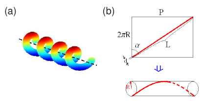
To begin with, we consider a helical wire (as shown in Fig. 1) where the diameter of the wire is , the radius of the helix is , the helical angle is , the pitch length of the helix is and the net length of one period is . The carrier density of the wire is denoted by . In the present work, we will focus on the case when the helical wire is sufficiently thin so that the electron motion can be considered as one dimensional, and then discuss later in detail the conditions imposed on the one-dimensionality.
In the continuum limit, the one-dimensional Hamiltonian of a single electron in the nano-helix is simply written as
| (1) |
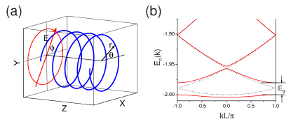
with the effective mass and the length coordinate of the helix. When a transverse electric field is applied, a potential energy term is induced in the Hamiltonian. To write it down explicitly, one can define the cylindrical coordinate system as shown in Fig. 2 (a), with the axis defined as the axis of the helix. The coordinate of a point with length coordinate is
| (2) |
—The Quantum Helical Transistor (QHT). When a transverse uniform electric field is applied, as shown in Fig. 2 (a), the potential energy is given by
| (3) |
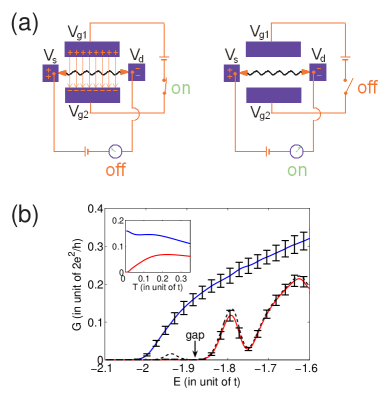
Thus the combined single electron Hamiltonian takes the form of . In this case, the continuous quadratic energy spectrum will split into energy bands, with first Brillouin zone . The typical band structure is shown in Fig. 2 (b). The gap between the th and th bands can be calculated by perturbation theory as in the limit . For concreteness, we shall focus on the first gap , since it is the largest, corresponding to . The transverse electric field can be generated by applying a voltage on the gate electrodes as shown in Fig. 3 (a). Assuming that the helical wire just fits into the gate electrodes, the resulting electric field is , and therefore the band gap is simply given by , which is independent of the radius of the helix. On the other hand, the average potential relative to the source-drain potential can be used to tune the chemical potential of the wire and thus the electron density . When the chemical potential lies in the first gap, the system is an insulator and the corresponding one-dimensional filling fraction is , that is, two electrons per helical period. The factor of two arises from the spin degeneracy.
Since the system with such a filling is gapless and conducting before applying electric field, the transverse electric field leads to a metal-insulator transition in the nano-helix, and thus defines a new type of nano-scale transistor switch, the status of which is “on” when the electric field is turned off, and “off” when electric field is turned on, as illustrated in Fig. 3 (a). Such a switch can work under a source-drain voltage , so that the chemical potential of both leads lie inside the gap.
To make our discussions here and below more concretive, we can regularize the Hamiltonian (1) to a tight-binding model:
in which is the lattice constant and is the total number of sites. The last term stands for quenched disorder, with the random potential . To study the transport properties in such a mesoscopic system, we need to include the effect of leads, which in this one-dimensional model can be described by the terms below:
| (5) | |||||
with and stands for the annihilation operators of electron in the left and right leads, respectively. Then the conductance can be calculated byLandauer (1957); Meir and Wingreen (1992)
| (6) | |||||
| (7) |
in which with the density of state on the fermi surface of each lead, and a factor from spin degeneracy has been included. For later convenience, the scattering amplitude is defined, in which are the local Weinner states on the left and right end site of the nanowire, respectively. is the retarded Green function of the nanohelix, . Under wide band approximation, the self-energy is .
The typical behavior of conductance is shown in Fig. 3 (b), in which the conductance with and without external electric field is compared. The metal-insulator transition induced by the electric field can be seen explicitly from the temperature dependence of the conductance, as shown in the inset of fig. 3 (b). Another important information from this calculation is that weak impurity can further widen the insulating region induced by electric field, since the electric-field induced subband is much narrower than the original energy band in the helix, and thus much easier to be localized by disorder. As shown in fig. 3 (b), under the same disorder strength, the first subband of the system with electric field is fully localized, while the one without electric field remains metallic.
However, a strong disorder can dominate the effect of electric field and thus kill this metal-insulator transition. Another important issue in this system is the elecron-electron interaction. According to the Luttinger liquid theory, repulsive interaction will make periodical potential more relevant and thus further stabilize this switch effectKane and Fisher (1992). In summary, the terms that may harm this effect are attractive interaction and strong impurity. Although we won’t involve more quantitative discussion in the present paper, a lower-limit estimate to the stability of the present effect can be given as , , with the characteristic energy scale of impurity random potential and phonon-induced attractive interaction, respectively. Under such a condition, the electric field-induced potential scattering dominant the interaction and impurity effect and thus the switching effect (and also the charge pumping and motor effect shown below) remains robust.
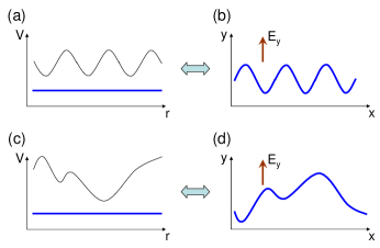
The device concepts discussed so far depend only on the periodically curved nature of the helical wire, and does not depend on the net helicity of the wire. Therefore, these concepts can be equally well implemented by patterning a quasi-1D wire in a periodically curved form, e.g. a sine wave form, on a plane, and by applying a transverse voltage. The helical wire perhaps has the advantage of being self-assembled and can be more easily realized in the nano-scale. In principle, the same idea can be generalized to design an arbitrary potential in a quasi-one-dimensional system. Consider a planar quantum wire with the shape of function in an uniform electric field , then the effective one-dimensional potential is determined by
| (8) |
in which is the arc length of the wire. In this way, one can obtain a quasi-one-dimensional system in any potential by choosing a proper shape , as shown in Fig. 4. Such a ”geometrical design” of one-dimensional systems takes the advantage of tunable strength and shape of potential energy, and thus can help to produce artificial one-dimensional materials with highly controllable electronic and optical properties. In particular, our device can realize a light-emitting-diode (LED) with tunable bandgap and color, controlled purely by the external gate voltage.
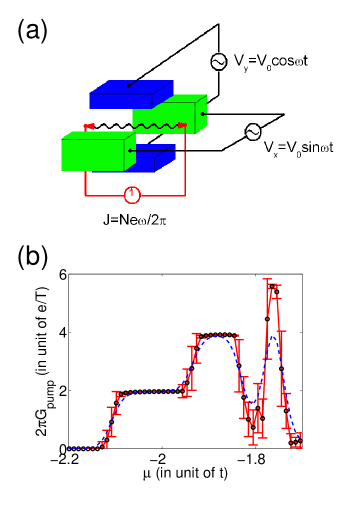
–The Quantum Helical Pump (QHP). We now consider an adiabatical rotation of the transverse electric field, when a more interesting effect emerges in the nano-helix system. Experimentally, the rotation of electric field can be realized by a set of quadrupolar electrodes, as shown in Fig. 5 (a). A rotating electric field with angular frequency is described by a time-dependent in the Hamiltonian (3). In the adiabatical limit , the gapped system with commensurate filling will stay in the time-dependent ground state. Similar to what ThoulessThouless (1983) proposed by using a sliding linear periodic potential, such an adiabatical translation of periodical potential on a gapped electron system can in general lead to a quantized charge pumping current
| (9) |
in the zero temperature limit, which means electrons per spin component are pumped through the wire system during each period . Intuitively, such a quantized charge pumping can be easily understood as a quantum version of Archimedean screw. Due to the electric force, the electron density in the lower subband is larger on the side nearer to positive electrode, and a charge-density-wave (CDW) is induced by the transverse electric field. Consequently, the high-density region will follow the rotation of electric field and thus the coordinate of each electron shifts by one pitch distance during one period of electric field.
More quantitatively, the current induced by a time-dependent electric field can be calculated in the tight-binding model (Field-induced Gap and Quantized Charge Pumping in Nano-helix) and (5) in a similarly way as the DC conductance:Brouwer (1998); Aharony and Entin-Wohlman (2002)
| (10) | |||||
A typical result of this calculation is shown in Fig. 5 (b). As expected by topological protection, random disorder can only induce fluctuation of for gapless system, and leaves the quantized plateaus unchanged. Actually, under zero temperature such a quantized adiabatical charge pumping is robust under any deformation of the Hamiltonian, as long as the subband gap is not closed. In particular, even if the two AC voltages applied to the quadrupolar electrodes are not perfectly harmonic but with some deformations or noises, as long as the electric field vector still encircles the point once each period, the quantization of pumping conductance (in the zero temperature limit) remains robust without any correction. In the same way it will remain robust when the nano-helix has a different shape as shown in Fig.1 (a) but with the same helical topology.
The pumping conductance at finite temperature is simply a convolution of the zero temperature result with the thermo factor . Consequently, will deviate from the quantized value. However, for a quantized plateu with width , the deviation at the middle-point of the plateu can be estimated by , which is exponentially small when .
Compared with the earlier experiments to realize Thouless’s charge pumping effect, like those involving surface accoustic waveShilton et al. (1996); Aharony and Entin-Wohlman (2002) or deformation potential on a quantum dotSwitkes et al. (1999), the present realization has the advantage of “coding” the topological information directly into the geometrical structure of the self-assembled nano-helix, whose long periodic structure makes the effect more intrinsic and robust. Our device could have higher precision of the current quantization and potentially lead to a new standard of current definition.Niu (1990)
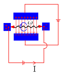
—The Quantum Helical Motor (QHM) As a direct inverse effect of the topological charge pumping, a nano-helix in a transverse electric field can work as a quantum motor, where a longitudinal current can lead to an uniform mechanical rotation with the frequency, as shown in Fig. 6
| (11) |
This is a direct quantum analog of a propeller or a windmill. In order to realize this effect, both ends of the helical wire should be attached to some kind of molecular swivel, similar to those described in Ref.Bryant et al. (2003), which enables the uni-axial rotation of the helix. It is also possible to drive an AC current through a helical wire with fixed ends, which will cause an AC oscillation of the helix. However, the AC effect is not as robust as DC effect, since the relation between AC oscillation and AC current is generally not protected by topological reason.
The relation (11) is generally true under any friction or other perturbations, as long as and so that the adiabatical evolution condition is satisfied. When there are more frictions, it will be harder to inject a current, but the relation between frequency and current remains valid. In the extreme case, if the nano-helix is fixed, then and at the same time , which recovers the switch effect. Suppose there is a frictional torque acting on the helix, then the energy cost per unit time is . Consequently, one needs a finite voltage to drive a constant current in this helix. The voltage is determined by the energy equilibrium condition , which implies that the power of the voltage cancels the friction energy cost. Thus we get the relation
| (12) |
which relates friction to a resistivity. As has been discussed in switch effect, the source-drain voltage must satisfy so as to keep the adiabatical evolution. Consequently, for a given friction , the rotating frequency of such a nano-motor is restricted by and also by the adiabatical condition .
—More discussions on experimental realizations
After proposing these three effects, we now analyze the detailed experimental conditions for their realizations:
-
1.
The system is quasi one-dimensional, which requires , , with the transverse excitation gap and the fermi energy.
-
2.
The electron (or hole) filling is commensurate .
-
3.
The adiabatical approximation is applicable, which requires (i) temperature ; (ii) impurity and attractive interaction energy scale ; (iii) rotation frequency of electric field or nano-helix .
-
4.
The total length of the nanohelix , so as to prevent the direct tunneling between the two ends and protect the topological transport.
To satisfy the requirements above, an ideal nano-helix for our purpose should have thin diameter , large helix radius , long length and also be very clean. Experimentally, two most possible candidates for this effect are helical nano-wires made from ZnO, SiC, CB, etc.Zhang et al. (2002); McIlroy et al. (2001); Zhang et al. (2003); Yang et al. (2004) and chiral biological molecules such as RNA, DNA and some proteins. To make the discussion more concrete, here we give an estimate of the present effects in the deformation-free ZnO nano-helix realized in Ref.Yang et al. (2004). The size of that nano-helix is reported as , , , (the estimate of is a little different from the previous one since the intercept of ZnO helix here is hexagonal rather than round.) If we approximate the electron effective mass by the bulk ZnO value Karpina et al. (2004), then the transverse excitation gap can be estimated as . The filling corresponding to first gap is , which in 3-d unit gives . The corresponding . Thus the condition is always satisfied, and condition requires the electric field or gate voltage . The in condition (4) is , thus the condition (4) is always satisfied. If we take an electric field or , then the conditions 3 requires i) ; ii) in condition 3, ; iii) . In summary, such an effect should be observable in a wide temperature range for the ZnO nanowire in Ref.Yang et al. (2004), if it is clean enough and the doping can be controlled well. (To avoid impurity effect, the filling should be controlled by gate voltage rather than chemical doping. )
Compared to the inorganic nano-helixes, chiral biological molecules such as RNA, DNA or protein may have the advantage of better one-dimensionality, which implies a larger transverse gap , since they can be much thinner than the nano-wires. For the effects proposed here to be observed, one needs to find molecules which are semi-conducting and have a good one-dimensional energy band. In a recent review articleEndres et al. (2006), transport properties of various DNA molecules are summarized, some of which show semiconducting behavior. If for some molecules , then it’s possible to observe the effect at room temperature with voltage .
In summary, in this paper we proposed three related effects in quantum helical systems under a transverse electric field. Under a slowly rotating electric field, a nanohelix with commensurate filling works as a quantum Archimedean screw. The experimental conditions to realize such effects are shown to be feasible for present experimental techniques. Since helical structures occur naturally in the biological world, the principles discussed here also provides new methods to control and detect biological molecules.
Acknowledgement. The authors wish to thank B. A. Bernevig, D. Cox, Y. Cui, S. Doniach, C. Huang, T. Hughes, S. Kivelson, C.-X. Liu, P. Wong and B.-H. Yan for useful discussions. This work is supported by the NSF under the grant No. DMR-0342832 and the US Department of Energy, Office of Basic Energy Sciences under contract No. DE-AC03-76SF00515.
References
- Zhang et al. (2002) H.-F. Zhang, C.-M. Wang, and L.-S. Wang, Nano Lett. 2, 941 (2002).
- McIlroy et al. (2001) D. N. McIlroy, D. Zhang, Y. Kranov, and M. G. Norton, Appl. Phys. Lett. 79, 1540 (2001).
- Zhang et al. (2003) D. Zhang, A. Alkhateeb, H. Han, H. Mahmood, D. N. McIlroy, and M. G. Norton, Nano Lett. 3, 983 (2003).
- Yang et al. (2004) R. Yang, Y. Ding, and Z. L. Wang, Nano Lett. 4, 1309 (2004).
- Xu et al. (2004) B. Xu, P. Zhang, X. Li, and N. Tao, Nano Lett. 4, 1105 (2004).
- Endres et al. (2006) R. G. Endres, D. L. Cox, and R. R. P. Singh, Rev. Mod. Phys. 76, 195 (2006).
- Thouless (1983) D. J. Thouless, Phys. Rev. B 27, 6083 (1983).
- Landauer (1957) R. Landauer, IBM J. Res. Dev. 1, 233 (1957).
- Meir and Wingreen (1992) Y. Meir and N. S. Wingreen, Phys. Rev. Lett. 68, 2512 (1992).
- Kane and Fisher (1992) C. L. Kane and M. P. A. Fisher, Phys. Rev. B 46, 15233 (1992).
- Brouwer (1998) P. W. Brouwer, Phys. Rev. B 58, R10135 (1998).
- Aharony and Entin-Wohlman (2002) A. Aharony and O. Entin-Wohlman, Phys. Rev. B 65, 241401 (2002).
- Shilton et al. (1996) J. M. Shilton, V. I. Talyanskii, M. Pepper, D. A. Ritchie, J. E. F. Frost, C. J. B. Ford, C. G. Smith, and G. A. C. Jones, J. Phys.: Condens. Matter 8, L531 (1996).
- Switkes et al. (1999) M. Switkes, C. M. Marcus, K. Campman, and A. C. Gossard, Science 283, 1905 (1999).
- Niu (1990) Q. Niu, Phys. Rev. Lett. 64, 1812 (1990).
- Bryant et al. (2003) Z. Bryant, M. D. Stone, J. Gore, S. B. Smith, N. R. Cozzarelli, and C. Bustamante, Nature 424, 338 (2003).
- Karpina et al. (2004) V. A. Karpina, V. I. Lazorenko, C. V. Lashkarev, V. D. Dobrowolski, L. I. Kopylova, V. A. Baturin, S. A. Pustovoytov, A. J. Karpenko, S. A. Eremin, P. M. Lytvyn, et al., Crystal Research and Technology 39, 980 (2004).