]Electronic address: mario.silveirinha@co.it.pt
Experimental Demonstration of a Structured Material with Extreme Effective Parameters at Microwaves
Abstract
Following our recent theoretical studies [M. G. Silveirinha, C. A. Fernandes, Phys. Rev. B, 78, 033108, 2008], it is experimentally verified that an array of crossed metallic wires may behave as a nonresonant material with extremely large index of refraction at microwaves, and may enable the realization of ultra-subwavelength waveguides.
pacs:
42.70.Qs, 78.20.Ci, 41.20.Jb, 78.66.SqThe design of novel materials with unusual electromagnetic properties has received a lot of interest in recent years, mainly because of the great potentials of structures with simultaneously negative permittivity and permeability Pendry (2000). However, materials with extreme parameters or extreme properties, such as near-zero-permittivity, extreme anisotropy, or very-large-permittivity may also have interesting applications in many problems such as tunneling through narrow channels and bends Silveirinha and Engheta (2006), subwavelength imaging Belov et al. (2006), realization of magnetic materials in the visible domain Rockstuhl et al. (2007), and cloaking Pendry et al. (2006).
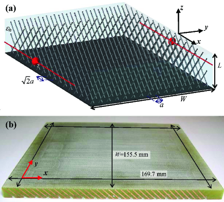
In a recent work Silveirinha and Fernandes (2008), we have reported that a composite material formed by crossed metallic wires may have an anomalously strong interaction with electromagnetic waves, and may enable the realization of materials with extremely large positive index of refraction. The geometry of a grounded slab of the structured material is depicted in the panel (a) of Fig. 1. It was theoretically predicted in Silveirinha and Fernandes (2008) that such grounded slab may interact with a wave with electric field polarized along the -direction as a material with very large permittivity. This result is rather surprising since systems formed by long metallic wires are typically thought as materials with permittivity. Here, we experimentally verify the results of Ref. Silveirinha and Fernandes (2008), and demonstrate that the proposed material may enable the realization of ultra-subwavelength waveguides.

To this end, a prototype of the structured material was fabricated using a layer by layer design and printed circuit techniques [panel (b) of Fig. 1]. In our planar design the metallic wires are replaced by printed metallic strips. The material is formed by an array of 97 layers of 1.6mm thick FR4 boards, for which the experimentally determined permittivity around the 1.3 GHz design frequency was with loss tangent . The boards of FR4 have been printed with parallel metallic strips with width mm. The metallic strips are tilted by with respect to the interfaces, and thus the strips in adjacent FR4 boards are mutually orthogonal. The lattice constant is mm, and the height of the substrate is mm. As illustrated in panel (a) of Fig. 1, the metallic strips are supposed to be connected with good ohmic contact to a metallic ground plane. In practice, such configuration may be difficult to reproduce using planar technology. To avoid this difficulty, we have mimicked the ground plane by printing an additional metallic strip running along the -direction at the lower edge of each FR4 board. This ensures good ohmic contact between all the strips in the same board. In addition, to ensure ohmic contact between the stacked FR4 boards, each FR4 board was perforated at 17 specific spots next to the lower edge [these spots can be identified in the lower panel of Fig. 1], and copper wires (running along the -direction) were inserted through these spots and soldered to the boards. Finally, the bottom face of the fabricated prototype was coated with a silver paint. Since the spacing between the copper wires is very small as compared to the wavelength, such configuration effectively behaves as a continuous ground plane.

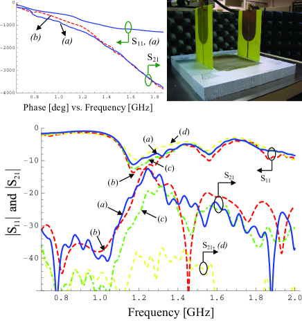
In order to characterize the properties of the material, we have investigated the propagation of transverse electric (TE) guided modes in the structured substrate. It is well known that a grounded dielectric slab with relative permittivity only supports guided modes when . Thus, a grounded substrate with the same permittivity as the FR4 boards only supports TE-guided modes for frequencies larger than 4.98GHz. As theoretically shown in Silveirinha and Fernandes (2008), the presence of the crossed wire mesh may result in a dramatic increase of the effective permittivity, and consequently in a significant reduction of the TE-modes cut-off frequency. In order to experimentally verify this property and measure the dispersion characteristic of the guided modes, the structured substrate was excited by an horizontal dipole antenna oriented along the -direction and placed 5mm away from the metamaterial substrate. The transmitted field was measured by an identical dipole placed at the other end of the substrate [top panel of Fig. 1]. Actually, the antennas used in the experiment were not wire dipoles, but instead were printed in FR4 boards as well. Each printed dipole is connected to the vector network analyzer (VNA) through a “balun” that makes the proper transition between the VNA coaxial cable and the co-planar printed line that feeds the dipole. In order, that the “baluns” are not detuned by the presence of the structured substrate it is convenient that the dielectric boards with the feeding circuit are oriented in such a way that they are normal to the -direction [top right panel of Fig. 2]. The free-space resonance frequency of the printed dipoles is approximately 1.2GHz.
The phase and amplitude of the measured S-parameters are depicted in the top left and lower panels of Fig. 2, respectively [curves (a)]. The calibration planes are at the antenna SMA connectors. Notice that is a measure of the fraction of power accepted by the input antenna, whereas is a measure of the coupling between the two dipoles. It is important to mention that even if there is an excellent coupling between the two dipoles the level of does not need to be close to 0dB, since part of the power accepted by the input antenna is either radiated as space wave, or dissipated in the dielectrics and metals, and only the remaining power is received by the test antenna, being the main propagation mechanism a guided wave. It is seen in Fig. 2 that for frequencies below 1.1GHz the level of is below -30dB, showing that for these frequencies the coupling between the dipoles is very low. This is understandable since for low frequencies the TE-guided modes are cut-off. However, around 1.25GHz there is dramatic increase of the level of which approaches -12dB, suggesting that the structure may support a guided mode above 1.25GHz, notwithstanding the electrically small thickness of the substrate (). This property stems from the anomalously high effective permittivity of the structured material Silveirinha and Fernandes (2008). For frequencies above 1.35GHz, the level remains significant, even though it deteriorates with increasing frequency, in part because the dipoles were tuned to 1.2GHz, and thus they tend to radiate poorly for frequencies relatively far from 1.2GHz. We have experimentally verified with a different set of printed dipoles tuned to 1.5GHz, that the onset of propagation of guided modes is still at 1.25GHz, whereas the level may be improved around 1.5GHz [not shown here]. Another reason for the deterioration of the level is that slightly above the cut-off frequency the guided modes become very confined inside the structured material, and thus it is difficult to launch the guided mode from the air region. This is supported by the extremely fast variation of the phase slightly above 1.25GHz, suggesting that the guided mode has an extremely short wavelength, and consequently is highly confined to the structured material because of the very large effective permittivity.
The reported experimental data concur very well with results obtained with a fullwave commercial electromagnetic simulator CST (CST Microwave Studio 2006, CST GmbH, http://www.cst.com) [curves (b) in Fig. 2]. In the numerical simulations the ground plane was assumed continuous. The excellent agreement between the numerical and experimental results demonstrate that our implementation of the ground plane effectively mimics an ideal continuous ground plane.
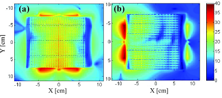
In order to show that the main propagation mechanism between the two dipoles is indeed a guided wave, we have placed an 80mm thick microwave absorber block in between the two antennas, 7mm above the prototype. The purpose of the absorber was to block the space wave radiated by the dipole. The corresponding measured S-parameters are shown in Fig. 2 [curves (c)]. It is seen that except near 1.25GHz, the level is little affected by the presence of the absorber, consistently with our expectations that the dominant propagation mechanism is the guided mode. The drop of the close to the cut-off is understandable, since at the cut-off frequency most of the energy of the guided mode propagates in the air region, and thus is also blocked by the absorber. To demonstrate in a conclusive manner, that the enhancement of the level is due to the emergence of guided modes, we have rotated the prototype by so that the dipole antennas become orthogonal to the FR4 boards with the printed strips. In this case, it is expected that the interaction of the metallic strips with the dipoles is very weak, and thus the prototype should behave in the same manner as an homogeneous grounded substrate with the same permittivity as the FR4 boards. The measured results corresponding to this scenario are depicted in the lower panel of Fig. 2 [curves (d)], and demonstrate that indeed the level is close to -40dB, consistently with the fact that a homogeneous dielectric substrate with , only supports TE-guided modes above 4.98GHz. The results obtained with CST Microwave Studio completely confirm these findings. In Fig. 3 we plot the total electric field amplitude at 1.25GHz along the mid-height cut of the structured substrate for the cases in which the dipoles are parallel to either the -axis or to the -axis. In these simulations the region in between the printed dipoles was not blocked by the microwave absorber. The plots demonstrate how in the case in which the dipoles are parallel to the FR4 boards (panel (a)), the wave is able to penetrate into the structured substrate permitting a good coupling between the two dipoles. This situation contrasts markedly with the case in which the dipoles are perpendicular to the FR4 boards (panel (b)), for which the guided mode cannot be launched and the wave cannot propagate along the substrate.


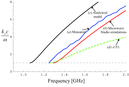
It is possible to calculate the dispersion characteristic of the guided modes from the experimental data. A straightforward analysis shows that the propagation constant of the guided mode, , is such that, , where is the width of the substrate [see Fig. 1], is a constant chosen so that at the cut-off frequency of the guided mode, and and are the and parameters referred to the input ports of the printed dipoles, respectively [these parameters are obtained by proper deembedding of the experimental data obtained at the antenna SMA connectors]. The extracted dispersion characteristic of the guided mode is depicted in Fig. 4 (blue curve). It was assumed in the extraction procedure that the cut-off frequency is 1.25GHz, consistent with the results of Fig. 2. In Fig. 4 we have also plotted the dispersion characteristic calculated with CST Microwave Studio CST (CST Microwave Studio 2006, CST GmbH, http://www.cst.com), obtained by analyzing a single cell of the periodic substrate (red curve), as well as the dispersion characteristic obtained using the analytical model described in our previous work Silveirinha and Fernandes (2008) (black curve) 111The model proposed in Silveirinha and Fernandes (2008) assumes that the inclusions are wires and not strips; we have taken the radius of the wires equal to , so that the perimeter of the cross-section of the inclusions is the same.. It is seen that the results obtained with the different methods concur very well, and that the value of may be significantly larger than unity for frequencies slightly above the cut-off frequency. This supports the fact the guided mode becomes highly confined in the structured material. In curve (d) of Fig. 4, we show the dispersion characteristic of a grounded dielectric slab, with the same cut-off frequency as the prototype. The permittivity of the equivalent dielectric slab is , which demonstrates how the crossed wire mesh may in fact enhance in a dramatic manner the electric properties of the host medium. As discussed in Silveirinha and Fernandes (2008), much larger values of the permittivity may be easily obtained by increasing the density of wires. It is interesting to note that the slope of vs. frequency is much larger for the structured material than for the equivalent dielectric slab. This property is a consequence of the fact that the response of the bulk structured material is anisotropic, even for propagation in the plane. Quite remarkably, this property enables a greater confinement of the electromagnetic fields inside the metamaterial slab, and thus suggests interesting applications of the proposed structure as an ultra-subwavelength waveguide. This work is supported in part by Fundação para a Ciência e a Tecnologia, grant number No. POSC/EEACPS/61887/2004.
References
- Pendry (2000) J. Pendry, Phys. Rev. Lett. 85, 3966 (2000).
- Silveirinha and Engheta (2006) M. Silveirinha and N. Engheta, Phys. Rev. Lett. 97, 157403 (2006).
- Belov et al. (2006) P. A. Belov, Y. Hao, and S. Sudhakaran, Phys. Rev. B. 73, 033108 (2006).
- Rockstuhl et al. (2007) C. Rockstuhl, F. Lederer, C. Etrich, T. Pertsch, and T. Scharf, Phys. Rev. Lett. 99, 017401 (2007).
- Pendry et al. (2006) J. B. Pendry, D. Schurig, and D. R. Smith, Science 312, 1780 (2006).
- Silveirinha and Fernandes (2008) M. G. Silveirinha and C. A. Fernandes, Phys. Rev. B 78, 033108 (2008).
- CST (CST Microwave Studio 2006, CST GmbH, http://www.cst.com) (CST Microwave Studio 2006, CST GmbH, http://www.cst.com).