Quantum theory of spontaneous emission in multilayer dielectric structures
Abstract
We present a fully quantum-electrodynamical formalism suitable to evaluate the spontaneous emission rate and pattern from a dipole embedded in a non-absorbing and lossless multilayer dielectric structure. In the model here developed the electromagnetic field is quantized by a proper choice of a complete and orthonormal set of classical spatial modes, which consists of guided and radiative (partially and fully) states. In particular, by choosing a set of radiative states characterized by a single outgoing component, we get rid of the problem related to the quantum interference between different outgoing modes, which arises when the standard radiative basis is used to calculate spontaneous emission patterns. After the derivation of the local density of states, the analytical expressions for the emission rates are obtained within the framework of perturbation theory. First we apply our model to realistic Silicon-based structures such as a single Silicon/air interface and a Silicon waveguide in both the symmetric and asymmetric configurations. Then, we focus on the analysis of the spontaneous emission process in a silicon-on-insulator (SOI) Slot waveguide (a 6 layers model structure) doped with Er3+ ions (emitting at the telecom wavelength). In this latter case we find a very good agreement with the experimental evidence [M. Galli et al., Appl. Phys. Lett. 89, 241114 (2006)] of an enhanced TM/TE photoluminescence signal. Hence, this model is relevant to study the spontaneous emission in Silicon-based multilayer structures which nowadays play a fundamental role for the development of highly integrated multifunctional devices.
pacs:
78.67.Pt, 78.20.Bh, 42.50.Ct, 42.70.QsI Introduction
It is well known that the environment surrounding an excited atom affects its rate of spontaneous emission (SE): enhanced SE in a resonant cavity was first predicted in the pioneering work by Purcell Purcell (1946) and, later on, an inhibited SE in a small cavity was shown by Kleppner Kleppner (1981). Such an effect can be explained either by classical electromagnetism, in terms of a self-driven dipole due to the reflected field at the dipole position, or in the framework of quantum electrodynamics, as emission stimulated by zero-point fluctuations of the electromagnetic field. As long as the coupling between the atom and the field is weak, both descriptions yield the same results Hinds (1994). In such a weak coupling regime, the SE rate can be calculated within first order perturbation theory by applying the Fermi’s Golden Rule, and is proportional to the local coupling of the atomic dipole moment to the allowed photon modes, i.e. to the local density of states (LDoS) van Tiggelen and Kogan (1994); Sprik et al. (1996). The modifications in the electromagnetic boundary conditions induced by the surrounding material alter the density of states as well as the SE rate: when the LDoS vanishes, then the SE process is inhibited, while, when an increase in the density of states occurs, the rate of SE can be enhanced over the free space value.
A large amount of work, both theoretical and experimental, has been devoted to the analysis of the SE from emitters (such as atoms, molecules or electron-hole pairs) embedded in dielectric environments of varying complexity. In an homogeneous medium with dielectric constant , it has been shown by Glauber Glauber and Lewenstein (1991) that the SE rate relative to the free space value, is enhanced when and reduced for , as it has been demonstrated also experimentally by Yablonovitch Yablonovitch et al. (1988). In spite of, or rather, thanks to its relative simplicity, the single interface has been subject of a constant research Drexhage (1974); Morawitz and Philpott (1974); Wylie and Sipe (1984, 1985); Khosravi and Loudon (1991); Janowicz and Zakowicz (1994); Snoeks et al. (1995); Barnes (1998); Inoue and Hori (2001); Wang et al. (2005) which still goes on, since it is the ideal system where experimental and theoretical analysis can be performed in order to get the basic understanding necessary to investigate more complex structures. The double interface has also been widely studied, especially as a waveguide slab, i.e., an high-index core surrounded by low-index cladding layers, with both a quantum electrodynamical Khosravi and Loudon (1992); Zakowicz and Bledowski (1995); Nha and Jhe (1996); Urbach and Rikken (1998); Ho et al. (1999) and classical Brueck (2000) approach. In systems characterized by more than two interfaces, both the technology and the theory needed become more demanding, but the expected effects turn out to be also more interesting. For instance, among multiple dielectric layers structures, planar microcavities have been subject of intense research in last years Bjrk et al. (1991); Rigneault and Monneret (1996); Rigneault et al. (1997); Benisty et al. (1998), due to their ability to considerably affect the density of states and thus strongly modify the emission into a particular mode, which is of crucial importance for the development of light emitting devices.
In this work we study the SE rate in a non-dispersive and lossless multilayer dielectric structure by applying a fully quantum electrodynamical formalism. With respect to previous published works, which generally deal with a specific dielectric structure, our main aim is to develop a model suitable for more than one configuration, thus taking into account all the possible modes (and the related SE rates) which can be excited in the examined structure. While our discussion tackles the problem of the spontaneous emission from a theoretical point of view, the results derived can provide a useful quantitative insight into the modifications of the atomic radiative processes which occur in realistic structures. As an example, we apply our method to evaluate the SE rate in silicon-based optical waveguides, which nowadays can be tailored according to different geometries, from simple waveguides (three-layers geometry) to multilayers-like configurations. These structures are characterized by a high index contrast and are able to confine and guide the light very efficiently in nanometer-size spatial regions as a result of total internal reflection. The waveguiding and confining properties, together with the low propagation losses (typical of Silicon) and the good compatibility with complementary metal oxide semiconductor technology, make them very attractive for the future development of highly integrated multifunctional optoelectronic and photonic devices (see e.g., Refs. Lee et al. (2001); Vlasov and McNab (2004); Almeida et al. (2004a)). Furthermore, with an embedded optically active layer, these structures can also be exploited as silicon-based optical sources. With this purpose, one of the most promising configurations recently proposed is the Slot waveguide Almeida et al. (2004b); Xu et al. (2004): this system consists of a thin (few nanometers thick) layer (slot) of low-index material bounded by two high-index material regions (typically Silicon), which are the core of an optical waveguide; the high-index contrast interfaces at the slot are able to concentrate the electromagnetic field in very narrow spatial regions (), thus leading to an enhancement in the radiation-matter interaction. A theoretical investigation Barrios and Lipson (2004) of the emission properties of a slot waveguide doped with Erbium ions and embedded in optoelectronic devices, as well as the experimental evidence Galli et al. (2006) of an enhanced light-matter coupling, have been already presented, but a full quantum mechanical analysis of the spontaneous emission processes in this kind of structures is still lacking. Here, we face this problem by applying the developed formalism to evaluate the SE rate of a dipole embedded first in a single Silicon/air interface, then in both a symmetric (high-index contrast) and an asymmetric Silicon waveguide, and finally in a Slot waveguide.
In order to build up a quantum electrodynamical theory of the SE process, the electromagnetic field must be first decomposed into the normal modes supported by dielectric structure under consideration. This is needed in order to set up a second quantized form of the electromagnetic field, and then to express the local density of states and SE rate by application of Fermi’s Golden Rule. The LDoS can be also derived within a quantum electrodynamic and Green’s function formalism as often done in the literature, using either a scalar or a dyadic Green’s function, see e.g. Refs. [Wylie and Sipe, 1984, 1985; Hooijer et al., 2001; Joulain et al., 2003]. In a generic multilayer structure, the normal set of modes, i.e., a complete and orthonormal set of solutions of Maxwell equations for the considered structure, is well known Yeh (1988) and consists of a continuous spectrum of radiative modes and a discrete one composed of guided modes, defined for both transverse electric (TE) and transverse magnetic (TM) polarizations not (a). Guided modes are trapped by the highest refractive index layer (if any), and are evanescent in both half spaces - the lower and upper cladding - surrounding the multilayer structure. Radiative modes can be either fully or partially radiative. The former, similar to free space modes, extend over the whole space and propagate out of the dielectric structure from both cladding layers as outgoing plane waves, while partially radiative modes propagate from the cladding layer with higher refractive index only, being evanescent (due to total internal reflection) along the lower refractive index cladding. The modes, found as the elementary solutions of Maxwell equations with proper boundary conditions, have more than one representation, since one needs to characterize the asymptotic behavior of the radiative states, such a characterization being not unique. The standard set of radiative modes, originally introduced by Carniglia and Mandel Carniglia and Mandel (1971), and which is generally applied to describe the interaction of a radiating system with the electromagnetic field in a dielectric structure, is not very convenient for SE analysis though. In this paper, we chose to apply a set of radiative modes characterized by a single outgoing component only. Such a choice leads to a simple definition of the LDoS for radiative states, avoiding the difficulties related to the treatment of the interference between different outgoing modes (see Refs. [Zakowicz, 1995; Glauber and Lewenstein, 1995]), which arise when the standard set of radiative modes based on the triplet incident-reflected-transmitted waves is used. Furthermore, the emission rates in the lower and upper half-spaces of a generic multilayer structures - or, in general, the SE patterns - can be easily calculated.
The paper is organized as follows. In Sec. II the field modes supported by multilayer dielectric structure are listed and described. We show that the basis of radiative states which has been used for the quantization of the electromagnetic field in the considered dielectric structure, can be obtained from the standard set of radiative modes by a Time-Reversal transformation. In Sec. III we perform a standard quantization of the electromagnetic field, and in Sec. IV a second quantized form for the atom-field interaction term of the whole system Hamiltonian is set up and then used (in the electric dipole approximation) to derive the expressions of the LDoS and the SE rate as a function of the dipole position. In Sec. V the spatial dependence of the SE rate will be examined for several structures of interest. A short summary of the results is given in Sec. VI.
II System and Field Modes
The system we are investigating is depicted in Fig. 1: it is made up of M dielectric layers (stack) which are parallel to the plane and assumed to be infinite along the and directions. Each layer is () thick and the surrounding media, i.e., the lower (layer 0) and the upper (layer M+1) claddings, are taken to be semi-infinite. Each of the media is supposed to be lossless, isotropic, and homogeneous along the vertical () direction. Hence, the dielectric constant is a piecewise constant function in the direction and it will be denoted as in each of the dielectric media.
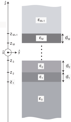
In order to develop a quantum theory for the spontaneous emission of a dipole embedded in such a dielectric structure, the classical electromagnetic modes, which are needed in the expansion of the electromagnetic field operators (see Sec. III), must be first specified. The modes are found as the solutions of the following eigenvalue problem
| (1) |
which results from the homogenous Maxwell equations for the electric and magnetic fields , having harmonic time dependence , and with the condition being fulfilled. The set of these fundamental modes is complete and orthonormal,
| (2) |
the orthonormality condition being expressed by
| (3) |
The electric field eigenmodes, which can be obtained from , are also orthonormal according to the following condition Carniglia and Mandel (1971):
| (4) |
Since the whole system is homogenous in the plane the field modes will be factorized as , where is the in-plane propagation vector.
In a lossless multilayer dielectric structure, the complete set of orthonormal modes consists of an infinite number of radiative modes and a finite number of guided modes. The former can be classified into two types. Fully radiative modes, akin to free-space modes, radiate in both the lower and upper cladding, while partially radiative modes radiate only in the cladding with the higher refractive index, propagating out of the smaller index cladding as evanescent waves with exponentially decreasing amplitude. Guided modes propagate along the dielectric planes only, being trapped (confined) by the highest refractive index layer and characterized by an evanescent field profile in both claddings.
Whereas the guided modes are completely specified by the Maxwell equations and the proper continuity conditions across the dielectric boundaries, the radiative modes are not, and their asymptotic behavior at infinity (when ) has to be characterized. Such a characterization, however, is not unique.
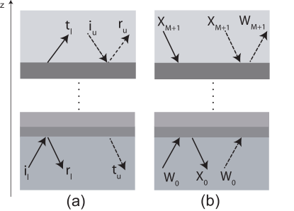
The standard choice for radiative modes [see Fig. 2(a)] assumes one incident wave incoming towards the stack of M layers either from the lower or from the upper cladding, and two outgoing waves, one being reflected (on the same side of the incoming one) from the stack and the other being transmitted (on the opposite side) across it. This set of modes, originally introduced by Carniglia and Mandel Carniglia and Mandel (1971) for the quantization of the electromagnetic field in a dielectric interface, is orthonormal and complete Białynicki-Birula and Brojan (1972) and it has been widely employed to characterize the radiative states in structures like dielectric waveguides Khosravi and Loudon (1992); Urbach and Rikken (1998) and planar dielectric microcavities Rigneault and Monneret (1996); Hooijer et al. (2001).
Such a choice, however, is not the most convenient when dealing with radiation emission analysis. As shown in Fig. 2(a), both the reflected and the transmitted components (the pairs and ), which belong to two different modes, contribute to the total emission in a given direction. As pointed out by Zakowicz Zakowicz (1995), the computation of the radiative density of states turns out to be problematic since the quantum interference between the two different outgoing modes has to be explicitly taken into account. Thus, interference terms must be considered when emission in either the upper or the lower layer is evaluated. As shown in the reply by Glauber and Lewenstein Glauber and Lewenstein (1995), interference effects cancel out only when the emission in the upper cladding layer () and in the lower one () are combined. To avoid this subtle interference problem, and to be able to calculate the fraction of emission in either the upper or the lower cladding layer, a more suitable way to define the radiative states in emission problems is to choose a set of modes based on a single outgoing wave. This component comes together with two incoming waves propagating towards the structure, as shown in Fig. 2(b) with the triplets and for states outgoing in the upper and lower cladding layers, respectively. By using this mode decomposition, the total emission signal is thus completely specified by one outgoing mode only - either by the component labeled as for radiative states outgoing in the upper cladding, or by the component for states outgoing in the lower cladding - and interference terms never arise.
It is worth to notice that this set of radiative modes can be obtained from the standard one previously discussed (which is specified in terms of the incoming waves) after application of Time-Reversal (TR) operator. A Time-Reversal operation transforms modes propagating along the positive -direction into modes propagating along the negative one, and therefore a mode incoming from the upper (lower) layer, into a mode outgoing from the upper (lower) layer. Hence, as from Figs. 2(a)-(b), the radiative modes and are the TR counterparts of the triplets and , respectively. Furthermore, since the algebraic properties are invariant under Time-Reversal operations, also the new set of radiative states is orthonormal and complete. The following rule for the Time-Reversal operation over a generic spatial mode propagating along the -direction with wavevector , can be established:
| (5) |
The transformation rule Eq. (5) applies to both fully and partially radiative modes: outgoing modes towards positive (negative) being (), specified by the real wavevector , keep the plane-wave-like character, turning into outgoing modes towards negative (positive ) (). The evanescent modes , characterized by the imaginary wavevector , keep the exponentially decaying profile after the transformation Eq. (5).
A mode decomposition characterized by a single outgoing component, like the one here described, has been already used to specify the radiative modes in dielectric interfaces Janowicz and Zakowicz (1994); Inoue and Hori (2001) as well as in slab waveguides Zakowicz and Bledowski (1995). It has also been used in the formally similar problem of diffraction losses in photonic crystal waveguides Andreani and Gerace (2006). Here, we extend its application within a quantum electrodynamical theory suitable to the analysis of radiation emission in generic multilayer structures.
In the following a detailed description of both guided and radiative profiles is given.
II.1 Radiative modes
As previously introduced, the set of radiative states consists of a single outgoing component propagating outward from the whole structure and two other waves propagating towards it. In each of the M layers the field is a superposition of two modes propagating in opposite directions (with respect to the -direction). The modes are specified and labeled by the propagation wavevector , where the -component in each of the M+2 media, is given by
| (6) |
Let us denote by the unit vector which is orthogonal to both and and set , with . With the implicit time dependence , the field profiles for TE polarization are given by
| (7) |
| (8) |
where is a normalization box-volume which disappears in the final results. The expressions for the amplitudes , and as well as the method used to obtain them are detailed in Appendix A.
For TM-polarized radiative modes the field profiles are given by:
| (9) |
| (10) |
where , and are given in Appendix A.
II.2 Guided modes
In order for the whole dielectric structure to support a set of guided modes, (at least) one of the dielectric constant () of the M inner layers has to fulfill the constraint
| (11) |
The guided modes, which are in-plane propagating and evanescent along the z direction, are labeled by the in-plane wavevector and the mode index [ if Eq. (11) holds] in a joint single index . By we denote the -component of the guided mode wavevector,
| (12) |
where is the frequency of the -th guided mode. In the upper () and lower () claddings is purely imaginary, where , and hence the mode field decays exponentially along the direction. In the following we give their explicit form, which results from a generalization of the standard waveguide field modes (see e.g. Refs. Yariv (1989); Andreani and Gerace (2006)).
III Field Quantization
In this Section the canonical quantization of the electromagnetic field in a non-uniform isotropic dielectric medium described by a piecewise constant permeability is performed Glauber and Lewenstein (1991); Bhat and Sipe (2006); Gerace and Andreani (2007). The electric displacement vector and the magnetic induction (a unit magnetic permeability is assumed) are simply given by the relations
| (17) |
The starting point is the quantization of the vector potential which is defined by the familiar relations
| (18) | |||||
| (19) |
We use here the generalized Coulomb gauge Glauber and Lewenstein (1991) defined, in absence of external charges, by the choice and the relation
| (20) |
which automatically satisfies the transversality condition on , , and is consistent with the equation of motion for the vector potential
| (21) |
In order to obtain a second-quantized Hamiltonian for the free photon field, we first introduce the classical Hamiltonian function , i.e. the total electromagnetic energy,
| (22) | |||||
where is a quantization volume, is the canonical momentum, and is the Lagrangian function from which Eq. (21) follows after Hamilton’s principle. The vector field operator is then expanded in normal modes:
| (23) |
where () are Bose creation (destruction) operators of field quanta with energies satisfying the usual commutation relations
| (24) |
being a generic index labeling the corresponding eigenmode characterized by the wavevector .
| (25) |
From Eq. (25) the following orthonormality conditions Carniglia and Mandel (1971); Glauber and Lewenstein (1991); Bhat and Sipe (2006) for the electric and magnetic fields follow:
| (26) |
| (27) |
Finally, from Eqs. (22) and (23), one gets the well known second-quantized form for the free photon field:
| (28) |
IV Emission Rates
In this Section the spontaneous transition rate of an excited atom embedded in a non-uniform dielectric medium is calculated. We suppose that the atom, located at position and initially in the excited state (having energy ) undergoes a spontaneous dipole transition to its ground state (having energy ) thereby emitting a photon of energy . The total Hamiltonian of such a system can be written as
| (29) |
where is the free-field Hamiltonian given by Eq. (28), is the free-atom Hamiltonian,
| (30) |
and is the atom-field interaction term which, in the electric dipole approximation and near the atomic resonance , reads J-Sakurai (1982) as
| (31) |
where and are the atomic down- and atomic up- transition operators, respectively, and is the dipole matrix element, being the atomic dipole operator of the atom located at . The electric field operator can be obtained from the vector potential operator through Eqs. (18) and (23),
| (32) | |||||
We assume that the interaction between the excited two-level system and the electromagnetic field in the dielectric medium is not too strong, so that the transition between two states can be studied within the framework of perturbation theory. Let us then consider the initial and the final states of the combined atom-radiation system: initially there are no photons and the atom is in the upper (excited) level, ; in the final state one photon is emitted in any mode of the electromagnetic field of frequency and the atom is in the lower (ground) level, . According to Fermi’s Golden Rule (see e.g. Ref. Loudon (1983)) the spontaneous emission rate of an atom located at position is
| (33) |
where and are th energies of the initial and final state, respectively. By insertion of Eq. (32) in the above expression, and using the commutation rules for and , the spontaneous decay rate finally reads
| (34) |
By taking into account the -th cartesian component of the eigenmode , the contribution to the total emission rate can be written as
| (35) |
where is the -th contribution to the local density of states (LDOS) van Tiggelen and Kogan (1994); Sprik et al. (1996) :
| (36) |
In a multilayer dielectric structure, an excited dipole can decay either as a radiative or a guided eigenmode. As discussed in Sec. II.1, the radiative modes are specified by the propagation vector of the outgoing component. Hence, in Eq. (34), and =() is a double index specifying the final state parameters, namely the field polarization and the cladding layer in which the emission occurs, for emission in the lower cladding and for emission in the upper cladding. For what concerns the guided modes, and =(), where is the guided mode index introduced in Sec. II.2. Furthermore, since the dielectric function is homogenous in each layer, the spontaneous emission rate will be expressed as a function of the coordinate only.
For both decay channels (radiative and guided) two contributions to the total emission rate can be distinguished: (i) the emission rate due to the decay of horizontal dipoles, i.e. in-plane oriented dipoles ( or ), which couple to both TE- and TM-polarized fields, (ii) the rate due to the decay of vertical dipoles () which interact with TM-polarized modes only. For randomly oriented dipoles, the total averaged emission rate can thus be written as . In the rest of this Section we derive the exact expressions for the emission rates into both radiative and guided modes.
IV.1 Emission rates into radiative modes
For each propagation wavevector the frequency of the radiative modes has to satisfy the relation
| (37) |
where () if the emission occurs in the lower (upper) cladding. With in Eq. (34), the emission rate into the radiative modes is thus given by
| (38) | |||||
where the TE- and TM-polarized fields and are given by Eq. (7) and (10), respectively. It is convenient to re-write the emission rate as a function of the LDoS for radiative states according to
| (39) |
whith
| (40) | |||||
and being the one-dimensional (1D) photon DoS at a fixed in-plane wavevector , for radiative modes outgoing in the medium :
| (41) | |||||
where is the width of the normalization box in the -direction (which disappears in the final expression of the SE rate) and [ if ] is the Heaviside function. It is worth to stress that, by using Eq. (40) with the basis of radiative states discussed in Sec. II.1, we get rid of any ambiguity in the definition of the LDoS: for each outgoing radiative mode ( or ) the LDoS is defined by a single mode-component only and thus any difficulty related to interference effects between components of different modes is avoided. Also, due to the Heaviside function in Eq. (41), emission into partially radiative modes occurs only in the cladding with the higher refractive index.
From Eqs. (39)-(41), and after the introduction of spherical coordinates in the space,
| (42) |
the single contributions to the total emission rate due to the decay of horizontal and vertical dipoles are easily obtained:
| (43) |
| (44) |
| (45) |
where the field amplitudes , and are given by Eqs. (51), (56) and (55), respectively.
IV.2 Emission rates into guided modes
According to Eq. (34), the spontaneous emission rate for the decay into guided modes having frequency is given by
where the fields and are given by Eq. (13) and Eq. (16), respectively, the sum extends over all the guided modes, and the 2D LDoS is given by
| (47) |
The emission rates , and can be easily obtained after integration over of Eq. (IV.2):
| (48) |
| (49) |
| (50) |
where , and are given by Eqs. (57), (63) and (62), respectively. In the expressions given above, and are the in-plane wavevector and the group velocity of the th guided mode calculated at the dipole emission frequency , respectively. The wavevectors as functions of the frequencies can be found as the poles (which are real ones for guided modes) of the transmission amplitude of the whole dielectric structure, being the total transfer matrix.
V Applications
In this Section we apply the formalism previously developed in order to investigate the SE process in realistic multilayer structures. As a typical high-index dielectric material, we take Silicon (nSi=3.48). After the analysis of a single Silicon/air interface, we will examine and compare the emission and confinement properties of different Silicon waveguides, namely a standard waveguide slab consisting of a Silicon core surrounded by two cladding layers with the same refractive index (symmetric configuration) or different ones (asymmetric configuration) and the silicon-on-insulator Slot waveguide. The SE rate has been evaluated for dipoles emitting at which is the typical emission wavelength of Erbium ions (Er3+) often used as the active layer of Silicon-based light sources (see e.g. the review paper by Kenyon Kenyon (2005)). All the rates shown have been normalized with respect to the vacuum emission rate of a randomly oriented dipole.
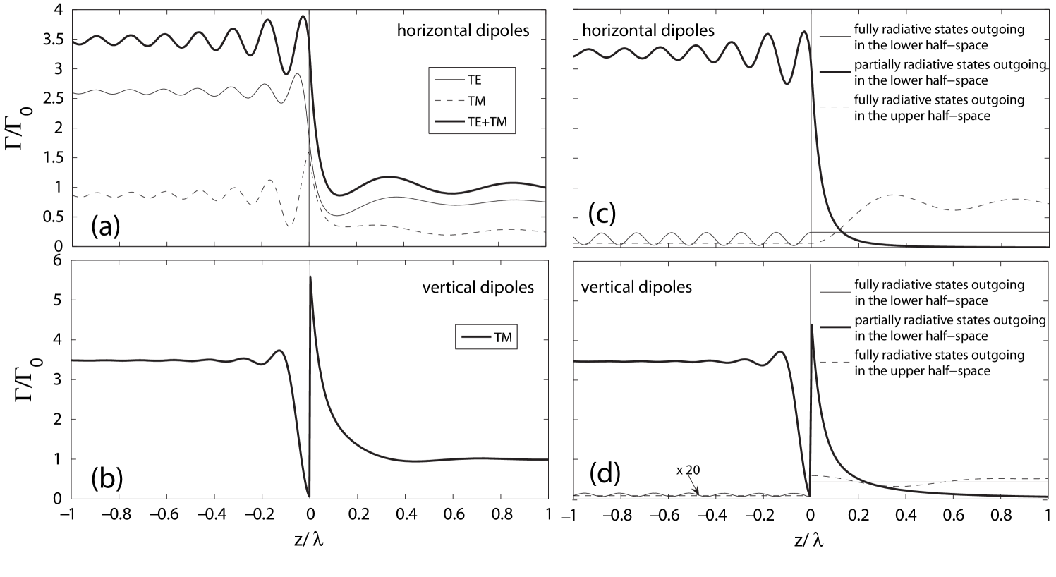

Figure 3 shows the normalized spontaneous emission for a Silicon/air interface as function of . The emission rate for horizontal dipoles decaying into TE- and TM-polarized modes [see Fig. 3(a)] varies continuously through the interface, as required from the continuity condition of the tangential field component at a dielectric boundary, while the emission rate for vertical dipoles (which couple to TM-polarized modes only), is discontinuous at the same point [see in Fig. 3(b)] due to the discontinuity of the component of the electric field. Far from the interface boundary, when , the spontaneous emission rate (for both horizontal and vertical dipoles) is scaled by the refractive index according to , in agreement with earlier works Glauber and Lewenstein (1991); Khosravi and Loudon (1991); Janowicz and Zakowicz (1994), with oscillations around the average value. The contributions to the total emission rate due to the decay into partially and fully radiative modes are shown in Figs. 3(c)-(d): in the dielectric half space the emission is mainly due to the partially radiative states (see the thick solid lines for ) which also characterize the profile of the total emission rate in the proximity of the interface boundary [see the thick solid lines at values between 0 and 0.2 in Figs. 3(a)-(c) and in Figs. 3(b)-(d)] and decay exponentially (in form of evanescent waves) in the free half space far from it. Hence, the evanescent component of partially radiative modes (which does not contribute to the total energy flux and it is hidden in standard far field experiments) turns out to be relevant in radiation emission analysis, since it strongly affects the radiative lifetime in the vicinity of the interface boundary. Moreover, for vertical dipoles in a generic dielectric/air interface, one can analytically work out that, in the limit of a very large refractive index , the emission into partially radiative modes (which is the dominant one) at the discontinuous boundary, is given by and , in agreement with an earlier work by Loudon Khosravi and Loudon (1991); not (b).
The contributions to the total SE rate corresponding to light emitted either in the lower or in the upper layer are shown in Fig. 4 as a function of the dipole position. It is worth to notice that, within our model, these quantities are straightforwardly obtained by selecting the single outgoing radiative mode (see Fig. 2 in Sec. II), through the index-layer (emission into the lower cladding) or (emission into the upper cladding) in Eq. (40). These rates could also be obtained by using the standard basis with a single ingoing and two outgoing components Carniglia and Mandel (1971), but in this case the interference terms between the two modes of Fig.2a must be explicitly calculated Zakowicz (1995). Thus, the present approach using the basis with a single outgoing component is especially useful for calculating radiative patterns and the emitted light in the lower/upper half spaces, which is a physically and technologically important problem for light emitting structures like LEDs and vertical laser diodes.
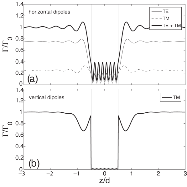
The spontaneous emission rates for a symmetric Silicon waveguide are shown in Figs. 5 and 6 as functions of , where is the thickness of the Silicon core () surrounded by air. Such a structure supports a finite number of guided modes and, since the upper () and lower () claddings have the same refractive index, only fully radiative modes can be excited and propagate out from the waveguide. By choosing a thickness , one can calculate 7 TE and TM guided modes whose contribution to the total emission rate is significantly greater than the contribution due to the emission into radiative modes, as it can be seen by comparison of Figs. 5(a)-(b) with Figs. 6(a)-(b). Furthermore, the emission rate in the core [see the spatial range in Figs. 5(a)-(b)] is close to the bulk value .
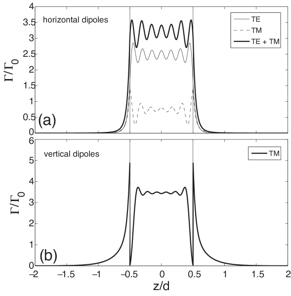
The influence of an increasing number of guided modes is investigated in Fig. 7, where the emission rate has been evaluated as a function of the so called dimensionless photonic thickness , while keeping the dipole position at the centre () of the waveguide. It can be noticed that, with increasing thickness , the contribution from the new arising modes is associated with the appearance of distinct features in the emission pattern such as dips and peaks.
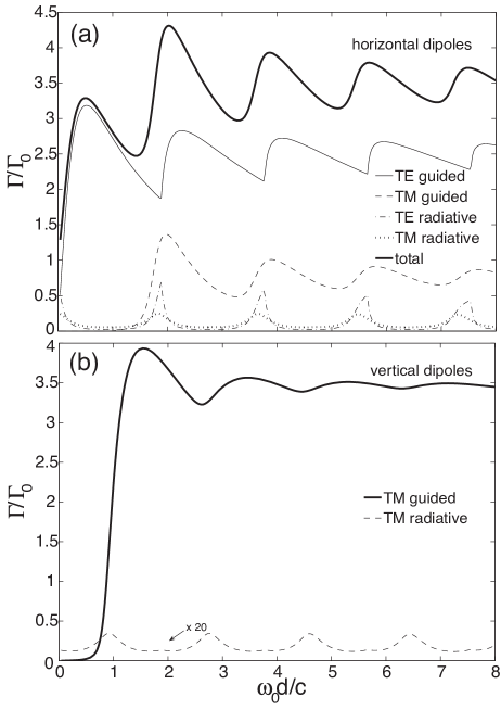
Furthermore, for vertical dipoles, the spontaneous emission rate is drastically suppressed for waveguide thickness below [see Fig. 7(a)], whereas, for the same range of thicknesses, the total emission rate from horizontal dipoles [see the thick solid line in Fig. 7(b)] is and mainly due the excitation of TE guided modes. Also, for thicknesses , the contributions to the total emission rate due to horizontal and vertical dipoles become comparable and close to the bulk value .
The above results, which follow from the mode decomposition based on a single outgoing component for radiative states (see previous Sec. II.1), are in agreement with those shown in earlier works Khosravi and Loudon (1992); Urbach and Rikken (1998); Ho et al. (1999) and which have been obtained by using the standard set of radiative modes based on the triplets incident-reflected- transmitted waves.
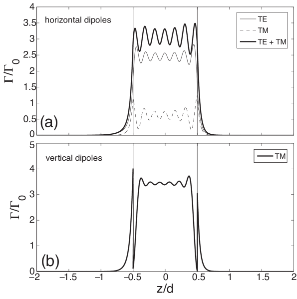
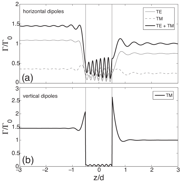
We now apply our model to study the SE in an asymmetric dielectric waveguide, i.e., a waveguide with different refractive indices in the lower and upper claddings (both values being of course smaller than the core one). Due to the asymmetry, the condition for total internal reflection can be met for incidence angles beyond the limit one, and also partially radiative modes, which are evanescent in the lower index cladding, can thus be excited in such a structure. Figures 8 and 9 show the dependence of the emission rates into guided and radiative modes, respectively, for an asymmetric waveguide made by a Silicon core bounded by a Silicon Oxide (SiO2) lower cladding, and by air in the upper half space acting as upper cladding. For a thickness , there are now 7 TE and 6 TM guided modes and the asymmetry-induced modifications in the emission pattern are clearly seen, especially for emission into radiative modes. Figure 10 shows the emission rate as a function of the core thickness: there are no guided modes for thicknesses smaller than and the emission rate is thus sustained by radiative modes only (see the continuous thick line). For the emission is mainly due to guided modes, the contribution from TE polarized modes being larger. However, as a consequence of slab asymmetry leading to partially radiative modes, the contribution from radiative states is larger than in the symmetric waveguide case.
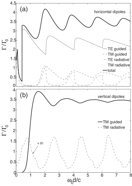
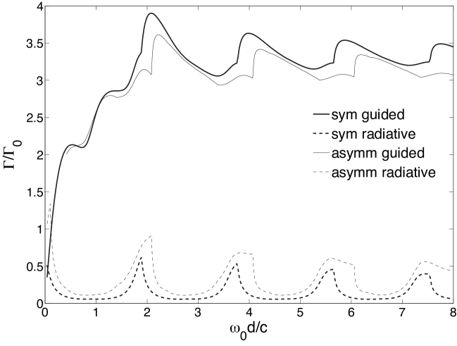
Figure 11 shows the averaged SE rate into guided and radiative modes for both the symmetric and asymmetric configurations previously analyzed, as a function of the core thickness. Here is the sum over the two polarizations for a planar (horizontal) dipole, while for a vertical dipole and the contributions from horizontal () and vertical () dipoles have been averaged as in the realistic case of a randomly oriented dipole in Si. Again, it can be seen that in the asymmetric slab case, the contribution of radiative over guided modes in the SE is increased, mainly due to the fact that the asymmetric slab supports partially radiative modes that contribute to SE and are taken into account explicitly in the present calculation.
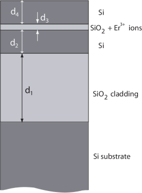
A stronger confinement effect can be achieved in a SOI slot waveguide. The core of such a waveguide (see the schematic in Fig. 12) is made up of a very thin layer (slot) of low refractive index active material (few tens of nanometers thick) embedded between two high-index material regions. In the configuration here considered, the core consists of a sequence of Si/SiO2 : Er3+/Si layers and lies on the top of a SiO2 cladding grown on a Si substrate. The discontinuity of the normal component of the electric field at the high-index-contrast interfaces of the slot gives rise to an increase of the LDoS, which in turn leads to an enhancement of SE rate into the waveguide modes.
In Fig. 13 the calculated SE rates into radiative and guided modes for a Si Slot waveguide are shown as a function of the dipole position (even if, in a practical case, the Er3+ emitters are located in the thin SiO2 layer). The effect of the discontinuity in the -component of the electromagnetic field at the slot interfaces can be clearly seen: the SE rate is mostly due to the decay of vertical (-oriented) dipoles into TM guided modes [see the dashed-dotted line in Fig. 13(b)], and the total emission into guided modes is about six times bigger than the corresponding emission into radiative modes [see the shaded regions in Figs. 13(a) and 13(b)]. Furthermore, after comparison with Fig. 11, it is evident that the light confinement is definitely more effective in a such a Slot waveguide than in a symmetric Si waveguide of any core-thickness.
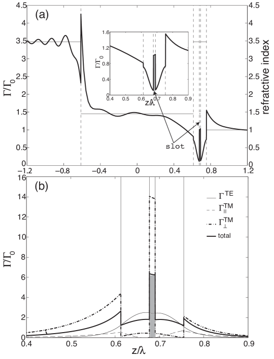
Moreover, the calculated SE rates shown in Fig. 13 allow to interpret the experimental results reported in Ref. Galli et al. (2006) for the enhancement in the photoluminescence from TM over TE polarized modes for a Slot waveguide containing Er3+ ions in the oxide (slot) layer. The vertical structure is the one depicted in our Fig. 12, with the same thickness parameters and the emission wavelength is 1.54 m. In the experiment, the TM/TE intensity ratio for light emitted from the edge of the waveguide is between 6 and 7.5, with a slight dependence on the position of the excitation spot. From Fig. 13, the calculated TM/TE ratio for a dipole embedded in the slot layer is around 7.8 (notice that the emission rate is dominated by , as the TM electric field component in the plane has a very small amplitude in the slot layer). Thus, the agreement between the theoretical results for the slot waveguide obtained within our model and the measurements of Ref. Galli et al. (2006) is quite satisfactory.
VI Conclusions
We have presented a quantum electrodynamical formalism in order to analyze spontaneous emission in generic lossless and non-dispersive multilayer dielectric structures. A second quantized form for the electromagnetic field, which follows after its expansion into normal modes, has been set up and used to derive the local density of states and express the decay rate as a function of the excited dipole position in the considered structure. The expressions derived have been used to study the spontaneous emission in Si-based waveguides of different geometries and with realistic parameters. The following conclusions summarize our results.
(i) The standard basis of radiative states generally used in the description of the electromagnetic field modes in a dielectric structure, based on incident/reflected/transmitted waves, is not the most appropriate one in radiation emission analysis as it leads to a subtle interference between different outgoing components Zakowicz (1995); Glauber and Lewenstein (1995). By choosing a set of modes specified by a single outgoing radiative component, the total emission rate as well as the emission in the upper/lower claddings (more generally, the SE patterns) can be calculated in a simple way, without any interference issue. One basis can be transformed into the other after application of the Time-Reversal operation.
(ii) The evanescent component of partially radiative modes which arise in any asymmetric configuration, i.e. when the upper and lower claddings have different refractive indices, is relevant for the SE analysis, as it can be seen in the single interface as well as in more complicated asymmetric structures.
(iii) We have calculated and compared SE rates for symmetric (air/Si/air) and asymmetric (SiO2/Si/air) silicon waveguides and shown that, in the latter configuration, the lower index contrast leads to an increased emission into radiative modes. Such an effect is much more evident in a silicon Slot waveguide: in this configuration the discontinuity of the normal component of the electromagnetic field which develops at the high-index-contrast interfaces of the slot layer, results into an enhancement of the local density of states for TM polarized guided modes. As an example, we have analyzed the SE rate in a Si Slot waveguide with the same structure parameters used in Ref. Galli et al. (2006) and found a very good agreement with the experimental evidence of the enhancement of the TM/TE photoluminescence. Thus, the model developed turns out to be a useful tool for the analysis of spontaneous emission processes in realistic structures such as SOI Slot waveguides. Further work will focus on analyzing more complex slot waveguides, as well as photonic crystal slab structures.
Acknowledgments
This work has been partially supported by the Piedmont Regional Project “Nanostructures for applied photonics (2004)” and by Fondazione CARIPLO. The authors are grateful to Fabrizio Giorgis (Politecnico di Torino) for encouragement and support and to Dario Gerace (Universit degli Studi di Pavia) for carefully reading the manuscript.
Appendix A Radiative modes
With reference to the geometry of Fig. 1, the field amplitudes of the TE-polarized radiative modes [see Eqs. (7) and (8) in Sec. II.1] are given by
| (51) |
| (52) |
| (53) |
For fully radiative modes outgoing in the lower (upper) cladding [see Fig. 2(b)], () in Eqs. (51)-(53) and the amplitude () obtained through the normalization condition Eq. (3) is given by (); all the other coefficients are then found by application of standard transfer-matrix theory. These results can be formally obtained by taking into account a normalization box having width in the -direction: when , being the thickness of the waveguide core or the thickness of a stack of layers in a generic multilayer structure, the contributions from the core/stack are of the order and are negligibly small as compared to the contributions from the semi-infinite cladding regions. Thus, the normalization of the radiative modes is determined by the cladding regions only, and the values given above are found for the amplitudes and . When the dielectric constants of the upper and lower claddings are different and the conditions for total internal reflection are matched, the modes become partially radiative. Without loss of generality, we assume . In this case, when , the emission occurs in the lower cladding only and the field becomes evanescent in the upper cladding, the component being purely imaginary. The field amplitudes are then found through the same conditions given above for the fully radiative modes, together with the transformation rule Eq. (5), i.e., by taking and replacing with its complex conjugate in Eqs. (51)-(53).
For TM-polarized radiative modes [see Eqs. (9) and (10) in Sec. II.1] the field amplitudes are given by:
| (54) |
| (55) |
| (56) |
Notice that defined in Eqs. (55), (56) have the same dimensions of defined in Eqs. (52), (53), while defined in Eq. (54) has the same dimensions of defined in Eq. (51). For fully radiative modes outgoing in the lower (upper) cladding, () and the normalization condition Eq. (3) yields () for the amplitude of the outgoing component. As for TE-polarized modes, all the other coefficients are straightforwardly found after a standard transfer-matrix calculation. For modes which are partially radiative in the lower cladding (evanescent in the upper cladding), one takes and replaces with its complex conjugate in Eqs. (54)-(56).
Appendix B Guided modes
The field amplitudes for TE-polarized guided modes [see Eqs. (13) and (14) in Sec. II.1]
| (57) |
| (58) |
| (59) |
where is a normalization surface which cancels in the final expressions for the emission rates, and the magnetic field is found by application of the Maxwell equation . The M+2 coefficients in the expressions Eqs. (57), (58) and (59) are found by solving the system consisting of M+1 relations which follow from the application of standard transfer-matrix theory and the orthormality condition Eq. (3) which leads to:
| (60) | |||||
with . For TM-polarized guided modes [see Eqs. (15) and (16) in Sec. II.1] the field amplitudes are given by
| (61) |
| (62) |
| (63) |
where the electric field is obtained from the relation . As for TE-polarized modes, the M+2 coefficients in the above expressions are derived within the transfer-matrix theory together with normalization integral Eq. (3) which yields the condition:
| (64) | |||||
References
- Purcell (1946) E. M. Purcell, Phys. Rev. 69, 681 (1946).
- Kleppner (1981) D. Kleppner, Phys. Rev. Lett. 47, 233 (1981).
- Hinds (1994) E. A. Hinds, Cavity Quantum Electrodynamics (Academic Press Inc., Boston, 1994).
- van Tiggelen and Kogan (1994) B. A. van Tiggelen and E. Kogan, Phys. Rev. A 49, 708 (1994).
- Sprik et al. (1996) R. Sprik, B. A. van Tiggelen, and A. Lagendijk, Europhys. Lett. 35, 265 (1996).
- Glauber and Lewenstein (1991) R. J. Glauber and M. Lewenstein, Phys. Rev. A 43, 467 (1991).
- Yablonovitch et al. (1988) E. Yablonovitch, T. J. Gmitter, and R. Bhat, Phys. Rev. Lett. 61, 2546 (1988).
- Drexhage (1974) K. H. Drexhage, Progress in Optics (North-Holland, Amsterdam, 1974), p. 163.
- Morawitz and Philpott (1974) H. Morawitz and M. R. Philpott, Phys. Rev. B 10, 4863 (1974).
- Wylie and Sipe (1984) J. M. Wylie and J. E. Sipe, Phys. Rev. A 30, 1185 (1984).
- Wylie and Sipe (1985) J. M. Wylie and J. E. Sipe, Phys. Rev. A 32, 2030 (1985).
- Khosravi and Loudon (1991) H. Khosravi and R. Loudon, Proc. R. Soc. London Ser. A 433, 337 (1991).
- Janowicz and Zakowicz (1994) M. Janowicz and W. Zakowicz, Phys. Rev. A 50, 4350 (1994).
- Snoeks et al. (1995) E. Snoeks, A. Lagendijk, and A. Polman, Phys. Rev. Lett. 74, 2459 (1995).
- Barnes (1998) W. L. Barnes, J. Mod. Opt 45, 661 (1998).
- Inoue and Hori (2001) T. Inoue and H. Hori, Phys. Rev. A 63, 063805 (2001).
- Wang et al. (2005) F. H. Wang, Y. P. Jin, B. Y. Gu, Y. S. Zhou, X. H. Wang, and M. L. Du, Phys. Rev. A 71, 044901 (2005).
- Khosravi and Loudon (1992) H. Khosravi and R. Loudon, Proc. R. Soc. London Ser. A 436, 373 (1992).
- Zakowicz and Bledowski (1995) W. Zakowicz and A. Bledowski, Phys. Rev. A 52, 1640 (1995).
- Nha and Jhe (1996) H. Nha and W. Jhe, Phys. Rev. A 54, 3505 (1996).
- Urbach and Rikken (1998) H. P. Urbach and G. L. J. A. Rikken, Phys. Rev. A 57, 3913 (1998).
- Ho et al. (1999) S. T. Ho, L. Wang, and S. Park, in Confined Photon Systems: Fundamentals and Applications, edited by H. Benisty, J.-M. Grard, R. Houdr, J. Rarity, and C. Weisbuch (Springer, Berlin, 1999), p. 243.
- Brueck (2000) S. R. J. Brueck, IEEE J. Sel. Top. Quantum Electron. 6, 899 (2000).
- Bjrk et al. (1991) G. Bjrk, S. Machida, Y. Yamamoto, and K. Igeta, Phys. Rev. A 44, 669 (1991).
- Rigneault and Monneret (1996) H. Rigneault and S. Monneret, Phys. Rev. A 54, 2356 (1996).
- Rigneault et al. (1997) H. Rigneault, S. Robert, C. Begon, B. Jacquier, and P. Moretti, Phys. Rev. A 55, 1497 (1997).
- Benisty et al. (1998) H. Benisty, R. Stanley, and M. Mayer, J. Opt. Soc. Am. A 15, 1192 (1998).
- Lee et al. (2001) K. K. Lee, D. R. Lim, L. C. Kimerling, J. Shin, and F. Cerrina, Opt. Lett. 26, 1888 (2001).
- Vlasov and McNab (2004) Y. A. Vlasov and S. J. McNab, Opt. Express 12, 1622 (2004).
- Almeida et al. (2004a) V. R. Almeida, C. A. Barrios, R. R. Panepucci, and M. Lipson, Nature 431, 1081 (2004a).
- Almeida et al. (2004b) V. R. Almeida, Q. Xu, C. A. Barrios, and M. Lipson, Opt. Lett. 29, 1209 (2004b).
- Xu et al. (2004) Q. Xu, V. R. Almeida, R. R. Panepucci, and M. Lipson, Opt. Lett. 29, 1626 (2004).
- Barrios and Lipson (2004) C. A. Barrios and M. Lipson, Opt. Express 13, 10092 (2004).
- Galli et al. (2006) M. Galli, D. Gerace, A. Politi, M. Liscidini, M. Patrini, L. C. Andreani, A. Canino, M. Miritello, R. Lo Savio, A. Irrera, et al., Appl. Phys. Lett. 89, 241114 (2006).
- Hooijer et al. (2001) C. Hooijer, G. x. Li, K. Allaart, and D. Lenstra, IEEE J. Quantum Electron. 37, 1161 (2001).
- Joulain et al. (2003) K. Joulain, R. Carminati, J. P. Mulet, and J. J. Greffet, Phys. Rev. B 68, 245405 (2003).
- Yeh (1988) P. Yeh, Optical Waves in Layered Media (John Wiley and Sons, New York, 1988).
- not (a) The word “radiative” is here used to identify a specific class of modes supported by a dielectric waveguide as commonly done in the literature, and does not embody all the spatial modes which contribute to the total radiative spontaneous emission. In the literature, “radiative” modes are also known as “traveling” modes in contrast with “guided” modes which are sometimes called “trapped” modes (Ref. 18).
- Carniglia and Mandel (1971) C. K. Carniglia and L. Mandel, Phys. Rev. D 3, 280 (1971).
- Zakowicz (1995) W. Zakowicz, Phys. Rev. A 52, 882 (1995).
- Glauber and Lewenstein (1995) R. J. Glauber and M. Lewenstein, Phys. Rev. A 52, 884 (1995).
- Białynicki-Birula and Brojan (1972) I. Białynicki-Birula and J. B. Brojan, Phys. Rev. D 5, 485 (1972).
- Andreani and Gerace (2006) L. C. Andreani and D. Gerace, Phys. Rev. B 73, 235114 (2006).
- Yariv (1989) A. Yariv, Quantum Electronics (Wiley, New York, 1989).
- Bhat and Sipe (2006) N. A. R. Bhat and J. E. Sipe, Phys. Rev. A 73, 063808 (2006).
- Gerace and Andreani (2007) D. Gerace and L. C. Andreani, Phys. Rev. B 75, 235325 (2007).
- J-Sakurai (1982) J. J-Sakurai, Advanced Quantum Mechanics (Addison-Wesley, Reading, 1982).
- Loudon (1983) R. Loudon, The Quantum Theory of Light (Clarendon Press, Oxford, 1983).
- Kenyon (2005) A. J. Kenyon, Semicond. Sci. Technol. 20, R65 (2005).
- not (b) Furthermore, it can be proved that, for a generic interface made by two dielectric half-spaces with index (at ) and (at ) and in the limit , and .