The microscopic study of a single hydrogen-like impurity in semi-insulating GaAs
Abstract
The charge dynamics of hydrogen-like centers formed by the implantation of energetic (4 MeV) muons in semi-insulating GaAs have been studied by muon spin resonance in electric fields. The results point to the significant role of deep hole traps in the compensation mechanism of GaAs. Electric-field-enhanced neutralization of deep electron and hole traps by muon-track-induced hot carriers results to an increase of the non-equilibrium carrier life-times. As a consequence, the muonium () center at the tetrahedral As site can capture the track’s holes and therefore behaves like a donor.
pacs:
72.20.Jv, 76.75.+iSemi-insulating (SI) GaAs is an important material that forms the basis of the GaAs microwave and integrated circuit industries. SI substrates are used for the growing of GaMnAs thin films, recognised as a prototype material for future spintronics devices Ohno_1998 . The semi-insulating properties of GaAs arise from the compensation of residual shallow donors, residual or intentionally added shallow acceptors and intrinsic or intentionally introduced deep centers. Deep centers may act as carrier traps, recombination centers or scattering centers, and have a strong influence on the electronic properties of the material even when their concentration is much less than the carrier density. Hence studies of deep level defects in GaAs is of both fundamental and applied interest.
Since the passivation of shallow acceptors and donors in GaAs by hydrogen was discovered in 1986 Johnson_1986 , the behaviour of hydrogen in III -V semiconductors has became the subject of intense research. Significant information on the microscopic properties of isolated hydrogen impurities have been obtained from muon spin rotation spectroscopy, where the behaviour of positive muons and muonium (Mu) are studied as an analogue of a light hydrogen isotope (m). In this letter we demonstrate that SR can be used to get alternative information on deep centers in GaAs.
Muonium in GaAs can exist in three charge states Mu+, Mu0 and Mu- Patterson ; Lichti_2007 . The stable position for Mu+ lies on the Ga-As bond (so-called Mu), with another possible location being the anti-bonding position close to As atom (ABAs). The tetrahedral void between four As atoms (TAs) is also considered Lichti_2007 as a metastable position supporting Mu+. Negative Mu- is usially placed at the tetrahedral position formed by four Ga atoms Mu, or at the anti-bonding position close to Ga atom (ABGa). Neutral muonium is believed to occupy the bond-center position (Mu) and both TGa and TAs tetrahedral sites and is thus denoted by Mu.
In semi-insulating and slightly doped n-type GaAs, the following is the accepted picture describing the distribution of muonium between the different states on a nanosecond time-scale following muon implantation. At low temperatures (T K) the diamagnetic fraction is small, while the Mu and Mu fractions are about 40(5)% and 60(5)% respectively. The Mu fraction remains constant up to at least room temperature, while the Mu fraction decreases above 100 K. This process is accompanied by a corresponding increase in the diamagnetic fraction, and is usually described in terms of Mu to Mu ionization Patterson (implying the thermal emission of the electron from the Mu to the conduction band). At low temperatures, electric field experiments Eshchenko_1999 ; Eshchenko_Cr_2002 have shown a gradual suppression of the Mu signal by the application of an electric field of the order kV/cm. The reduction of the Mu fraction is accompanied by a corresponding increase in the diamagnetic signal; however, electric fields of up to 20 kV/cm have no effect on the Mu signal. In this letter we show that very small electric field of kV/cm can effect long term ( s) dynamics of the neutral muonium.
Most of the experiments reported here were performed at the ISIS pulsed muon facility, located at the Rutherford Appleton Laboratory (RAL, Chilton, UK), using the novel technique of radio-frequency (RF)-SR in electric fields EF-RF-SREshchenko_RF . RF experiments are essentially longitudinal magnetic field () measurements, where the initial direction of the muon spin is co-linear with the relatively large (in our case about kOe) magnetic field, with a small ( Oe) RF field applied perpendicular to the at a frequency tuned to match the Zeeman splitting of the diamagnetic species ( MHz). Diamagnetic states formed from a paramagnetic precursor, even on a microsecond timescale, will contribute to the precessing RF asymmetry asymmetry, and consequently RF techniques have become a well established tool for studying the dynamics of slow muonium to diamagnetic conversion Morozumi_1986 . Our previous EF-SR experiments in insulators Eshchenko_2002 demonstrated that the muon is surrounded by its own track products, with the main radiation damage (the majority of electron-holes pairs) being behind the stopped muon. In the flat geometry we are using, by choosing the polarity of the applied electric field (parallel or anti-parallel to the muon track direction) one can select the appropriate charge (electrons or holes) for the long range interactions with the stopped muon. Thus EF-RF-SR Eshchenko_RF enables the selective (electrons vs holes) study of the dynamics of the interaction of muonium with hot carriers on a microsecond timescale. Since the stopped muon is a single probe at the end of his own track, the dynamics of track products will be determined by the intrinsic properties of the sample under the study e.g by deep centers. In this respect, SR experiments may offer a unique insight on the fundamental non-equilibrium properties of deep centers.
For SR measurements, 100% spin-polarized positive muons are implanted into the sample and the positron decay products monitored. Due to parity violation, the positrons are emitted preferentially along the instantaneous direction of the muon spin. Using two sets of positron counters placed upstream and downstream of the sample (backward and forward counters) the time-differential asymmetry of the muon decay is constructed in the standard way as , where and are decay counts in the backward and forward detectors respectively. The maximum asymmetry for the apparatus depends on the positions and solid angles of the detectors and, in our case, is about 0.23. Each SR spectrum contains at least several million decays. Four sets of histograms are collected: RF field on, positive electric field; RF field on, negative electric field; RF off, positive electric field; RF off, negative electric field. The positive electric field points parallel to the initial muon momentum. The states were changed every 1/50 s at every ISIS accelerator frame (i.e. before every muon pulse)

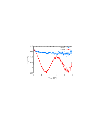
Typical SR spectra measured in GaAs are presented in Fig. (1). The RF off asymmetry spectrum consists of a fast-relaxing MuT fraction and a slow-relaxing signal which is the sum of the Mu and diamagnetic components. The contributions of these two components are resolved in the RF spectrum, where the diamagnetic fraction is seen in the precessing signal (which has a slow relaxation due mainly to the space inhomogeneity of the RF field) while the non-relaxing Mu is observed as a constant offset in the spectra.
Studies reported here were performed using a commercial high resistivity GaAs substrate ( Ohmcm, n-type conductivity with an electron mobility cm2/Vs), 0.5 mm thick, with the crystallographic axis perpendicular to the surface impacted by the muon beam. The sample was purchased from the American Xtal company, where it was grown using the vertical boat (VB) technique. Silver electrodes of 80 nm thickness were deposited on both surfaces of the sample using the DC magnetron sputtering technique, thereby making two Schottky contacts. This allowed us to apply voltages of up to 1 kV in both polarities, giving us a nominal electric field in the sample of up to 20 kV/cm.
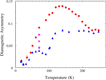
A measurement of the diamagnetic fraction in zero electric field is shown in Fig. (2).

The triangles represent the temperature dependence of the RF diamagnetic asymmetry in the virgin sample (no electric field history). This dependence is similar to that reported in the literature Hitti_2000 ; Lichti_2007 . The increase in the asymmetry is described in terms of Mu to Mu conversion. Above 120 K the RF asymmetry remains constant, and is in good agreement with the Mu fraction measured in transverse magnetic field experiments at low temperatures Patterson . This implies that in this sample below 250 K there is no contribution to the diamagnetic fraction from conversion of the Mu state, a conclusion in agreement with Lichti_2007 . The picture changes drastically if, at low temperatures, the sample is treated by applying a large ( kV/cm) electric field simultaneously with muon implantation. The enhanced diamagnetic RF asymmetry is shown by the circles. Above 70 K, the diamagnetic asymmetry in the treated sample exceeds that of the high temperature fraction measured in the virgin sample, implying an additional channel for Mu muonium to a diamagnetic state conversion is opened by the sample treatment. Measurements were carried out at a fixed temperature of 70 K to evaluate how the sample changes from its virgin condition to the treated state as a function of exposure to the muon beam. Results are shown by the stars in Fig. (1), each corresponding to a zero electric field measurement carried out after a further 30 minutes of treatment in a field kV/cm. To complete the transition, about two hours of beam exposure or electron-hole pairs per cubic centimeter are required. The enhanced RF asymmetry passes through a broad maximum around 120–140 K (a state that persists for at least 12 hours), while at temperatures above 140 K it shows annealing behavior and on warming to 220 K the sample is returned to the virgin state.
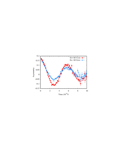
The origin of the enhanced diamagnetic RF signal can be understood from the electric field measurements. Typical SR spectra measured in the treated sample in electric fields 1 kV/cm are presented in Fig. (3).

Small negative electric fields reduce the precessing RF amplitude to the value measured for the virgin sample, while small positive electric fields have no effect on the amplitude. Taking into account the direction of the effect (positive electric fields point parallel to the incoming muon beam) and recognizing that the injected track carriers are positioned around and mostly behind the stopped muon, the reason for the enhanced diamagnetic signal seems likely to arise from the interaction between the track holes and the Mu species. A negative electric field will pull holes away from the stopped muon, thereby reducing the muonium to diamagnetic conversion, while a positive electric field will pull out the nearest holes but push ”early” track holes towards the stopped muon and muonium to to diamagnetic conversion is unchanged. In the virgin sample, a small electric field does not change the RF precessing asymmetry.
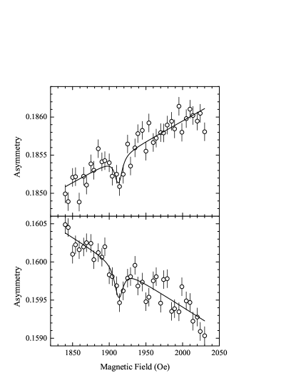
To identify the lattice position of the diamanetic species involved in the enhanced state, muon-nuclear level crossing measurements LCR experiments, were perfomed at the Paul Scherrer Institute, Switzerland. For Mu the main resonance in our geometry (H parallel to ) is expected around 1920 Oe Chow_2005 ; for Mu the resonances are observed at Oe Chow_1995 . For a treated sample we failed to record any resonance in the field range of Mu. Resonances were, however, detected at a field of 1913 Oe for treated SI-GaAs at K, and results for both small positive and negative electric fields are presented in Fig. (4). The resonance amplitude does not depend on the direction of the electric field, suggesting that the enhanced diamagnetic signal does not belong to the Mu state (at least during the time window of SR measurements s). We therefore need to consider that the tetrahedral As void may be supporting the Mu state.

The semi-insulating properties of the commercial vertical boat (VB) GaAs substrates are achieved by the compensation of shallow (residual or intentionally added) centers by the deep native centers. There are two main models discribing the compensation mechanism. A widely accepted theory Holmes_1982 suggests that the compensation can be attributed to the interaction between the deep intrinsic donors EL2 (an AsGa-related defect which is present at the level cm-3), residual donors (usually Si) and shallow carbon acceptors which are intentionally introduced in GaAs at the level of cm-3. However, the Fermi level (EF) is often found to lie below the EL2 midgap level, implying the existence of deep acceptor defects which can act like hole traps. Thermally stimulated (TS) current in conjunction with TS Hall effect measurements Bourgoin_1996 have demonstrated that the concentration of the deep hole traps in SI-GaAs is of the same order as the concentration of the deep electron traps, and that the pinning of the Fermi level on the EL2 midgap may be explained as a result of the balance between deep electron and hole traps.
The capture of electrons by the EL2+ traps occurs over a configuration barrier with energy of eV Martin_1979 . The applied electric field increases the energy of the carriers and results in enhanced phonon-assisted trapping over the configurational barrier. A similar behavior is observed for the holes traps. Capacitance spectroscopy measurements Prinz_1983 have revealed that at low temperatures ( K) a strong electric field ( V/cm) causes an increase of both electron and hole capture cross sections by five orders of magnitude for the deep traps in GaAs.
Based on these conclusions, the following model for the formation of the enhanced diamagnetic state measured in SI-GaAs is proposed. At room temperature, the initial state of the sample is characterized by ionized residual shallow donors, partially ionized EL2 traps and filled by electrons or ”ionized” deep acceptor levels (empty holes traps) and ionized shallow acceptor centers. Muon implantation at low temperatures results in the production of non-eqilibrium track carriers (electrons and holes) inside the sample. If a large electric field is applied, these carriers are transported through the bulk of the sample and are effectively captured by deep traps. At low temperatures the thermal emission of electrons/holes from deep traps is negligible, and consequently the sample is transfered to a metastable-like state. If the traps are filled, the life-times of non-equilibrium carriers are increased and the track electrons/holes can interact with the neutral Mu on a microsecond time scale. By considering how small electric fields of opposite polarity affect muonium to diamagnetic state conversion one can conclude that muonium interacts with the its own track holes. As the temperature in increased, electrons and holes are emitted from the filled deep traps, life-times for the excess carriers are reduced and there are no holes available to promote state conversion regardless of the sign of the applied electric field. The essential part of this model is the presence of both types of deep traps. In contrast, if one follows the simplest model of the SI-GaAs compensation mechanism (where only one deep EL2 electron trap is involved) then the electric field treatment will result to the filling of these traps and the excess hole life-time would not increase.
In conclusion, we have used the SR technique in combination with electric fields and RF measurements to probe non-equilibrium carrier dynamics in SI-GaAs. Below 120 K, the simultaneous bipolar injection (from the muon beam) and treatment of the sample with high electric fields results to the neutralization of both electron and hole deep traps. In the neutralized sample, excess holes from the muon track can be captured by muonium specied formed in the void created by the tetrahedral cage of four As atoms, where it acts as a filled donor. Our results point to the scenario where not only deep EL2 centers but also deep hole traps are involved in the compensation mechanism in SI-GaAs.
This work was partially performed at ISIS Pulsed Muon Source, United Kingdom, and at the Swiss Muon Source Facility of the Paul Scherrer Institute, Villigen, Switzerland.
References
- (1) H. Ohno, Science 281, 951 (1998).
- (2) N.M. Johnson, R.D. Burnham, R.A. Street, and R.L. Thornton, Phys. Rev. B 33, 1102 (1986).
- (3) B.D Patterson, Rev. Mod. Phys. 60, 69 (1988).
- (4) R.L. Lichti, H.N. Bani-Salameh, B.R. Carroll, K.H. Chow, B. Hitti and S.R. Kreitzman, Phys. Rev. B 76, 045221 (2007).
- (5) D.G. Eshchenko, V.G. Storchak , and G.D. Morris, Phys. Lett. A 264, 226 (1999).
- (6) D.G. Eshchenko, V.G. Storchak, J.H. Brewer, R.L. Lichti, Phys. Rev. Lett. 89, 226601 (2002).
- (7) D.G. Eshchenko, V.G. Storchak, B. Hitti, S.R. Kreitzman, J.H. Brewer, K.H. Chow, Physica B 326, 244 (2003).
- (8) Y. Morozumi, K. Nishiyama, and K. Nagamine, Phys. Lett. A 118, 93 (1986).
- (9) D.G. Eshchenko, V.G. Storchak, J.H. Brewer, G.D. Morris, S.P. Cottrell and S.F.J. Cox, Phys. Rev. B 66, 035105 (2002).
- (10) B. Hitti, S.R. Kreitzman, R. Lichti, T. Head, T.L. Estle, D. Wynne, E.E. Haller, Physica B 289-290, 554 (2000).
- (11) B.E. Schultz, K.H. Chow, B. Hitti, R.F. Kiefl, R.L. Lichti, and S.F.J. Cox, Phys. Rev. Lett. 95, 086404 (2005).
- (12) K.H. Chow, R.F. Kiefl, W.A. MacFarlane, J.W. Schneider, D.W. Cooke, M. Leon, M. Paciotti, T.L. Estle, B. Hitti, R.L. Lichti, S.F.J. Cox, C. Schwab, E.A. Davis, A. Morrobel-Sosa, and L. Zavieh, Phys. Rev. B 51, 14762 (1995).
- (13) D.E. Holmes, R.T. Chen, K.R. Elliott, and Kirkpatrick, Appl. Phys. Lett. 40, 46 (1982).
- (14) R. Kiliulis, V. Kazukauskas, and J.C. Bourgoin, J. Appl. Phys. 79, 69511 (1996).
- (15) A. Mitonneau, A. Mircea, G.M. Martin, D. Pons, Rev. Phys. Appl. 14, 853 (1979).
- (16) V.Ya. Prinz and S.N. Rechkunov, Phys. Stat. Sol. (B) 118, 159 (1983).