Characterization of a Single Crystal Diamond Pixel Detector in a High Energy Particle Beam
Abstract
Diamond has been developed as a material for the detection of charged particles by ionization. Its radiation hardness makes it an attractive material for detectors operated in a harsh radiation environment e.g. close to a particle beam as is the case for beam monitoring and for pixel vertex detectors. Poly-crystalline chemical vapor deposition (CVD) diamond has been studied as strip and pixel detectors so far. We report on a first-time characterization of a single-crystal diamond pixel detector in a 100 GeV particle beam at CERN. The detectors are made from irregularly shaped single crystal sensors, 395m thick, mated by bump bonding to a front-end readout IC as used in the ATLAS pixel detector with pixel sizes of 50 400 m2. The diamond sensors show excellent charge collection properties: full collection over the entire detector volume, clean and narrow signal charge distributions with a S/N value of 100 and a hit detection efficiency of (. The measured spatial resolution for particles under normal incidence in the shorter pixel direction is (8.9 0.1) m.
keywords:
Particle tracking detectors; Solid state detectors; Materials for solid-state detectors1 Introduction
The innermost tracking devices of the LHC detectors ATLAS [1] and CMS [2] have to cope with very intense particle radiation. Fluence levels of up to 1015 particles per cm2 are projected for the innermost pixel layers during the LHC lifetime [1]. Such large particle fluences cause damage to standard silicon pixel sensors, most dominantly by: (a) the trapping of moving charges which reduces the signal, (b) an increase in the effective doping concentration Neff which changes the space charge in the detector substrate material, and (c) an increase of detector leakage currents. The LHC semiconductor tracking detectors have been designed and built to stand these challenges for the LHC life time [1, 2, 3, 4]. Plans for an upgrade of the LHC luminosity by an order of magnitude to the Super-LHC (sLHC) are already underway and with it the projected radiation levels will rise considerably. As a consequence new types of sensors for pixel detectors need to be developed which are capable of coping with the expected radiation fluence to 1016 particles per cm2. For such radiation levels standard planar silicon pixel detectors may not be suited. Poly-crystalline diamond sensors, produced by chemical vapor deposition (CVD), have been exposed to radiation levels of 1.8 1016 protons per cm2 [5] with the conclusion that, with the measured S/N figures and the ability to run at comparatively (to Si) low threshold settings, diamond is an attractive sensor material for large radiation fluences. Single-crystal samples have recently been shown to follow the same damage curve as poly-material [5]. Hence diamond, in either mono- or poly-crystalline form, is an interesting material for tracking detectors operating close to the interaction point or in radiation harsh environments close to a beam line. Other benefits of diamond as sensor material are (a) its small dielectric constant ( = 5.7, = 11.9) which results in smaller input capacitances per area than for silicon, and (b) its complete absence of leakage currents, which is due to its large band gap (5.5 eV). Both of these facts lead to lower noise figures than for comparable silicon detectors. Electron and hole mobilities in CVD-diamond are large (1800 cm2/Vs and 1600 cm2/Vs, respectively) leading to fast collection times. In addition, diamond is an excellent thermal conductor, a property which can possibly be exploited for intelligent integrated cooling concepts of pixel vertex detectors.
While poly-crystalline CVD (pCVD) diamond can be grown in wafer scale sizes [6, 5] and large pixel detector modules have been built [6], the grain structure of the pCVD growth process causes effects which hamper a homogeneous and smooth charge collection in comparison to depleted silicon substrates. Trapping and recombination centers limit the carrier life time and hence the distance over which moving charges can induce a signal on the pixel electrodes. In addition, horizontal polarization fields, superimposed on the external drift field, can be generated by charges trapped at the grain boundaries. Nevertheless, charge collection distances above 300m have been measured in pCVD diamond sensors [7].
Recent advances in the production of diamonds by chemical vapor deposition has lead to single-crystal CVD (scCVD) diamond sensors with sizes larger than 1 cm2 [7] and thicknesses of up to 700 m [7]. The production process is still in its development and the sensors often come in irregular shapes. scCVD detector material is believed to be superior in terms of charge collection and homogeneity than poly-crystalline diamond sensors.
Poly-crystalline diamond pixel detectors have been constructed by means of using the bump bonding and flip chip techniques as single chip devices and also as multi – chip module detectors[8, 6]; they have been tested in particle beams[6, 7]. In this paper we report on a first-time characterization of scCVD pixel sensors using a high energy particle beam.
2 Single crystal diamond pixel detector
Single crystal diamond is fabricated using a CVD process on a single crystal substrate [9]. Currently larger scCVD structures often come in irregular shapes of a few cm2. Their charge collection properties have been measured in [5] showing full charge collection for thicknesses as large as 800 m with biasing fields below 0.1 V/m [7]. For unirradiated devices, no effect on the charge collection by pumping has been observed [7] indicating that trapping of charges plays no or only a minor role in scCVD detector devices, in contrast to pCVD devices.
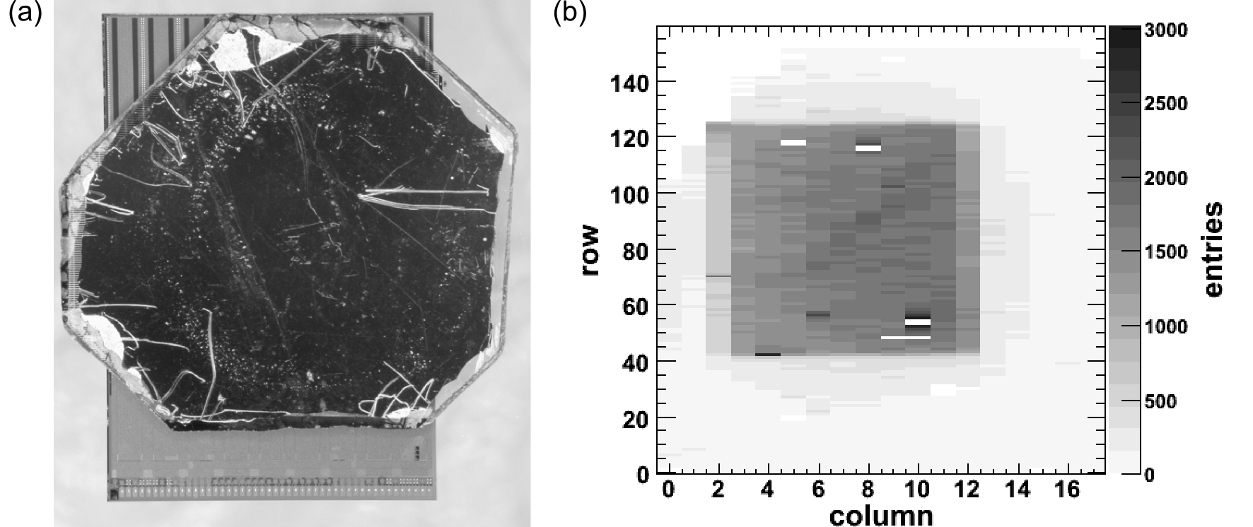
Our single-crystal diamond pixel detector (sensor plus electronics chip) is composed of an irregularly shaped scCVD diamond sensor with a homogeneous thickness of 395 m. Both sides are metallized (Ti/W). One side is segmented into a 50400m2 pixel pattern to match the pattern of the ATLAS pixel frontend chip (FE-I3 [12]). Solder (PbSn) bumping and flip-chipping technology at IZM (Berlin) [10, 11] has been employed to mate both parts. Figure 1(a) shows the assembly after bump bonding. Due to the irregular shape of the sensor only about 2200 of the 2880 possible pixels of the FE-I3 chip are covered by a corresponding sensor cell.
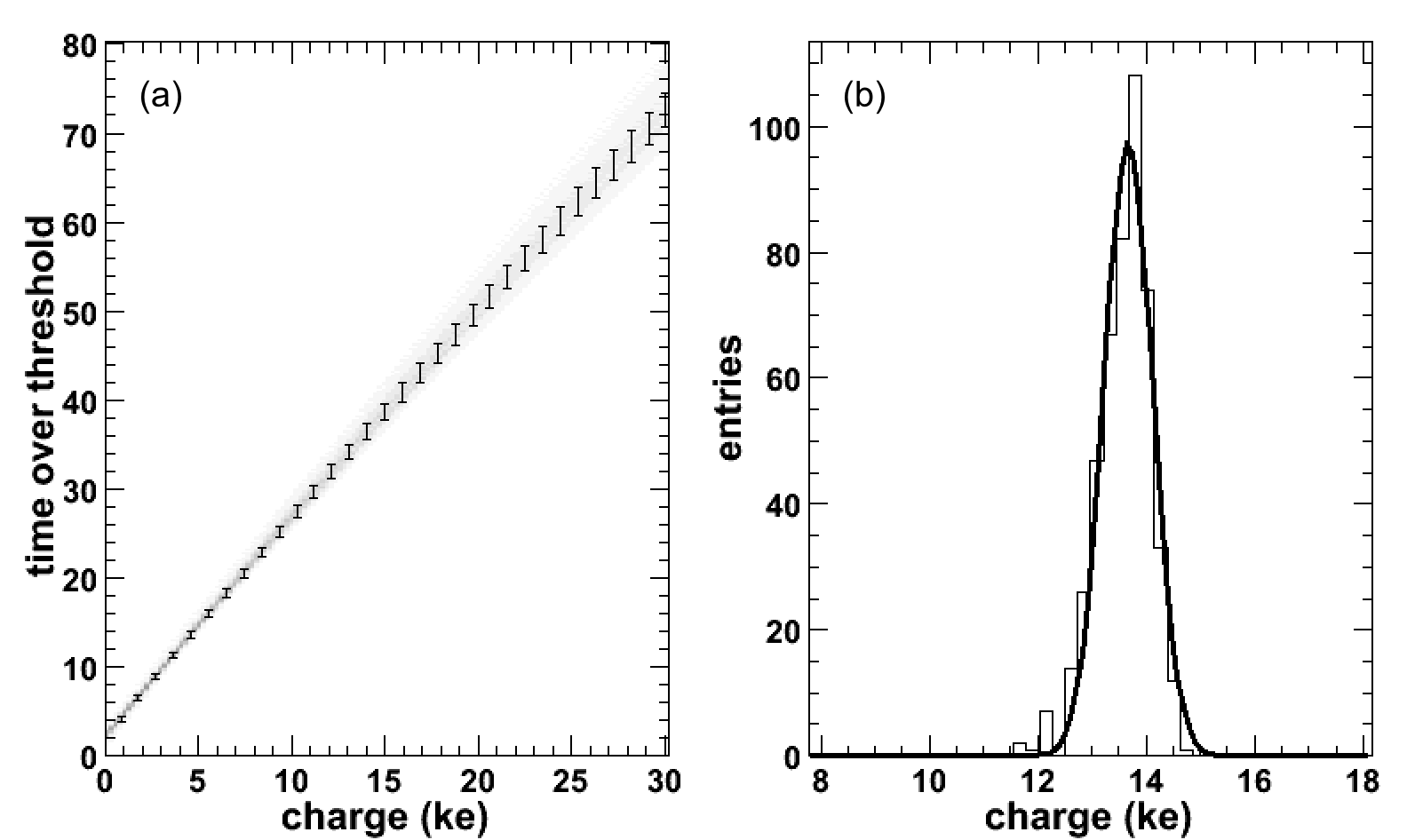
In this paper we particularly study the response of the scCVD diamond pixel device to high energy particles in terms of charge collection, spatial resolution and response homogeneity. The ATLAS pixel electronics provides zero suppression in the readout with a typical threshold level of 3000 - 4000 e- and a noise of 160 e- [3] when used with silicon detectors. As diamond sensors are basically free of leakage currents and have lower input capacitance, the sensor was operated at thresholds of about 1700e- with a noise level of about 130 e-, as determined from fitting the threshold curves of the pixels (s-curves). Analog information is obtained via the in-pixel measurement of time-over-threshold (ToT) with an approximate resolution of 8 bit [12]. The ToT-calibration is obtained for every pixel individually, by fitting the ToT response to input pulses injected over a capacitance of 41.4 fF. Figure 2(a) displays the calibration curves superimposed for all pixels. The band is the area of all calibration curves superimposed, the error bars are the rms spread of the calibration at a given charge. In fig. 2(b) the distribution of the input charge for a fixed ToT value of one pixel is shown. The mean value is 13700, the fitted is 500 e-. Note that it is larger than the noise value of 136 e-, because the ToT measurement receives contributions from leading and trailing edge uncertainties. The calibration uncertainty is estimated to be in the range of 5 – 10 . This calibration is used for the determination of the charge measurement in the tested devices.
3 Test beam setup at the CERN SPS
The scCVD diamond device has been tested in a 100 GeV pion beam at the CERN SPS. The setup is shown schematically in fig. 3. The device under test (DUT, the scCVD detector) was placed in between two pairs of silicon microstrip detectors [13]. The microstrip telescope was developed for ATLAS and consists of double sided silicon microstrip detectors with 50m pitch strips on both sides rotated by 90∘ with respect to each other. The S/N for the p-side, measuring the DUT x-direction, was 37 and the S/N for the n-side, measuring the DUT y-direction, was 22. Hits are read out zero suppressed and events waiting for read out can be buffered for some time [13]. The latter option was, however, not used. The telescope- and DUT-planes are triggered by the coincidence signal of two scintillators, placed in front and behind the setup. The precision obtained in the plane of the DUT is about 5 m in both spatial directions. The beam divergence is measured to be less than 0.2 mrad. The beam incidence angle with respect to the DUT plane is at most 1∘. The average data taking rate was limited by the readout system to around 50-60 Hz.
Only tracks from events with a single hit in each of the telescope planes were selected for the characterization measurements. Hits in the scCVD device were accepted if the seed position of the cluster is found in the predicted pixel or in a neighboring or next to neighboring (for the short pixel dimension) pixel. Otherwise it is counted as a miss in the detector efficiency calculation.
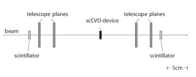
Figure 1(b) shows the hitmap in the plane of the characterized scCVD device in the test beam. The upper left corner, in which the FE-chip is not covered by the sensor is clearly visible as well as the shadow of the scintillation trigger counters illuminating the DUT with an almost quadratic profile. Two pixels had no bump contact and less than 20 were masked off during operation because they were noisy or impossible to tune to the low threshold setting.
4 Results
Charge collection and cluster size
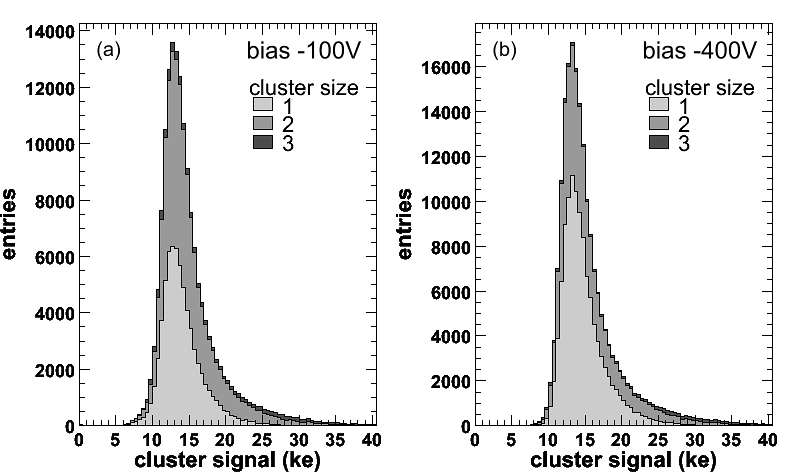
The diamond sensor can be operated with a fairly large range of biasing voltages. Unlike in silicon the electric field inside the sensor is fairly uniform for good crystals [14]. Over the area that could be investigated (i.e. covered by beam and electronics) the response of the detector was uniform for bias voltages larger than 100 V (0.25 V/m). As the drift velocity is directly proportional to the field, higher fields cause faster charge collection and hence a smaller spread of the charge cloud by diffusion. This is illustrated in fig. 4 where the measured charge distributions are plotted for fields of roughly 0.25 V/m in (a) and 1V/m in (b), respectively.
For high energy pions of 100 GeV, the mean energy loss in diamond due to ionization is about 10 larger than for particles in the minimum of the Bethe-Bloch curve [15]. Also the ratio between mean and most probable value of the charge distribution (Landau distribution) is thickness dependent and differs from that observed in silicon for the same thickness. For thicknesses between 200m and 400m the distribution for diamond is narrower than for silicon by 5–10. To estimate the most probable energy loss and charge deposit in our device and compare it with the calibrated charge measurement, we have followed[15] and the detailed descriptions given in [16]. Attempted calibration cross referencing by using standard radioactive sources for silicon detectors (e.g. 241Am or 57Co) turned out to be very difficult with the limited ToT charge resolution due to the much larger Compton contribution to photon absorption in diamond in comparison to silicon and the appearance of several nearby emission lines in many of these sources.
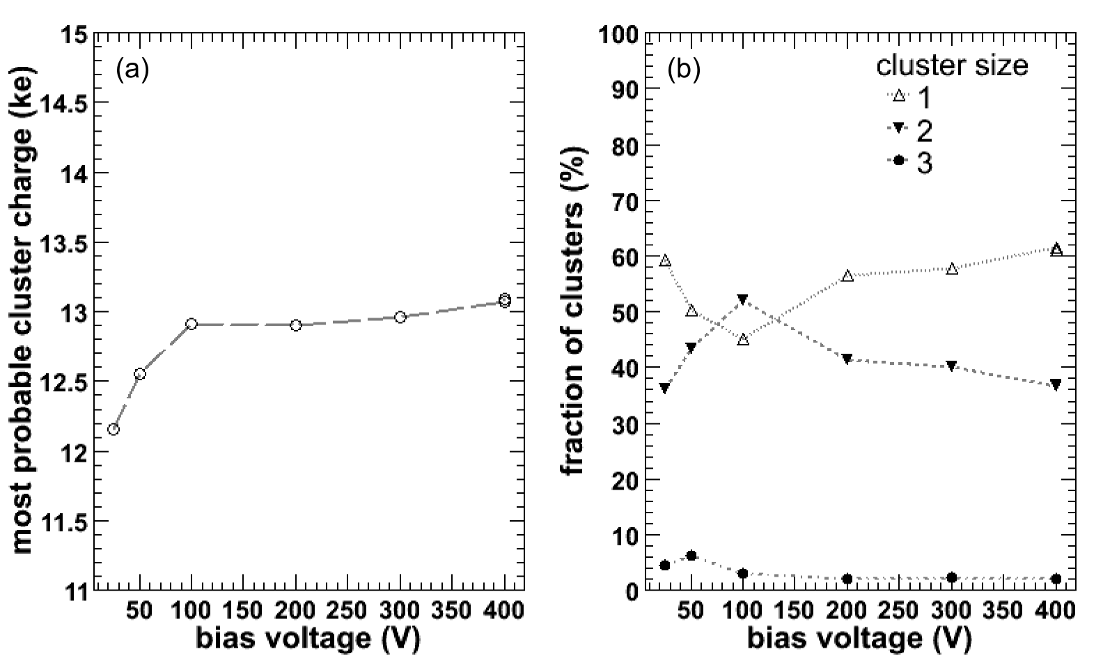
We adopt the information given in [16] to estimate the charge deposited in our scCVD diamond sensor by 100 GeV pions. For a thickness of 395 m the mean energy loss in carbon for a minimum ionizing particle is 1.725 MeV cm2/g. With the density for diamond of 3.52 g/cm3 and a mean energy for e/h creation of 13.1 eV, we find the most probable value (MPV) of the charge distribution by scaling the dependence on the thickness as given in [16] for silicon by the respective density ratio. Hence we expect a most probable charge value in the scCVD sensor of 13900 e-. The measured value, using the ToT to charge calibration outlined above, yields 13100 e- at 400 V bias voltage (fig. 4(b)), in fair agreement with the expectation within the calibration uncertainty (5 – 10). We note also that for ATLAS silicon pixel modules with the same readout chip it has been observed [17] that the absolute calibration to the 241Am 59.6 keV line in Si came out low by 8 which indicates that the charge injection capacitance may deviate from its design value by this amount. However, other explanations are conceivable. If one corrects the measured peak value for this mismatch the agreement with the expectation is within a few percent. The full width at half maximum in fig. 4(b) is 4000 e-, 30 of the MPV. The theoretical value following [16] is 4200 e-. With different shadings also the contributions from different cluster sizes to the Landau-type shape are indicated in fig. 4. The spatial charge distribution (charge cloud) becomes narrower for higher voltages, resulting also in a larger fraction of single pixel clusters at higher bias voltages. Figure 5(a) shows the measured MPV as a function of bias voltage. The curve saturates for bias voltages above about 100 V, indicating that for this single crystal diamond device the charge collection is complete. A small increase towards high biasing voltages is still observed and expected since for higher fields the probability of single pixels clusters increases rendering charge losses below neighbor pixel thresholds less likely.
Figure 5(b) shows the fractional decomposition of clusters (in Y direction) as a function of the bias voltage, showing that for full charge collection and low thresholds single and double hit clusters have roughly equal sharing (60:40).
The overall efficiency to find a hit near a track point (i.e. within 5x3 pixels, asymmetric due to the rectangular pixel size) extrapolated on the plane of the DUT is found to be .
Space point reconstruction
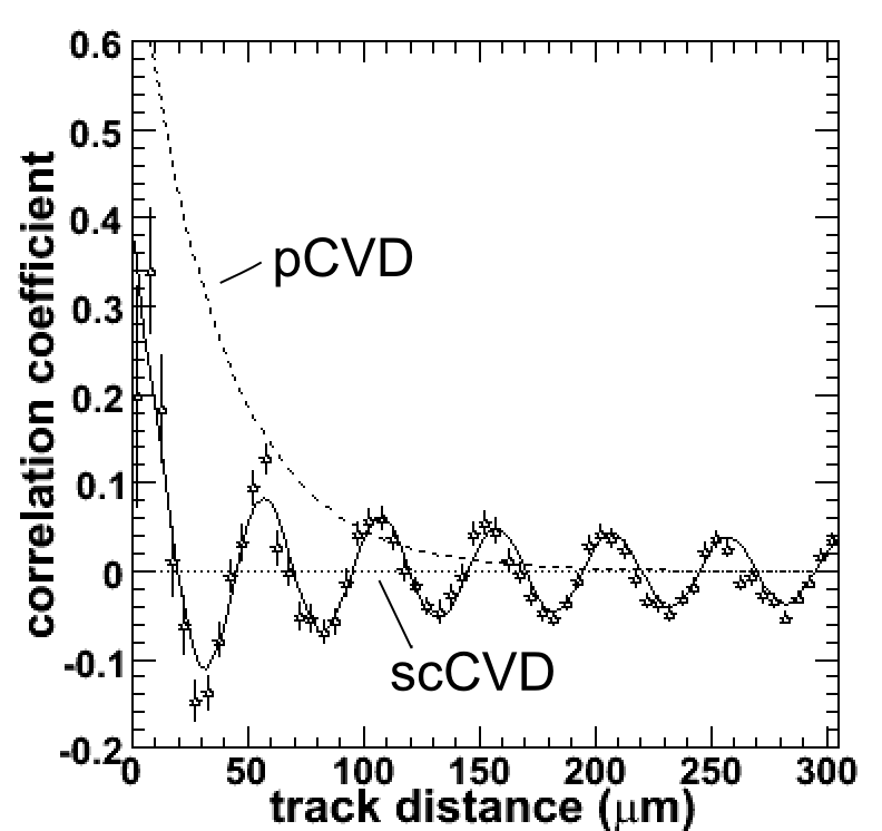
In previous studies of poly-crystalline diamond [18], the pCVD grain structure and the trapping of electric charges at their boundaries which may cause horizontal polarization fields, were identified as one explanation that affects the charge collection and thus the space point reconstruction in pCVD devices. As in [18] we plot in fig. 6 the correlation of the reconstructed Y coordinates (corresponding to the short 50 m pixel dimension) of the measured hits of two nearby tracks taken in different events, as a function of the distance of the tracks’ impact points (as determined from the telescope extrapolation). The sinusoidal shape of this distribution reflects the pixel pitch of 50 m, damped by a radial distance effect. The data are well fitted by a functional form sin exp, with being consistent with zero. In [18], albeit with a rather poor quality pCVD sensor compared to present standards, it was shown that in comparison with silicon, pCVD diamond – as a consequence of the pCVD grain structure – showed a net correlation developing for small two track distances and a correlation length 36 m for the exponential term was measured. This effect, observed in [18], is indicated by the dashed line in fig. 6. The measurements presented here for 400 V bias voltage now demonstrate that for single crystal diamond such a net correlation no longer exists, i.e. no evidence for horizontal polarization fields are observed.
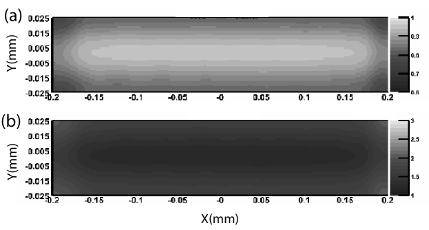
We show in fig. 7 that proper sharing of signal charge is observed in scCVD diamond pixel sensors as it is in silicon sensors. In fig. 7(a) the fractional signal charge in the pixel with the largest charge of a hit-cluster (seed pixel) is shown as a map over the pixel area. Fig. 7(b) is the corresponding map of the cluster size (number of pixels above threshold).
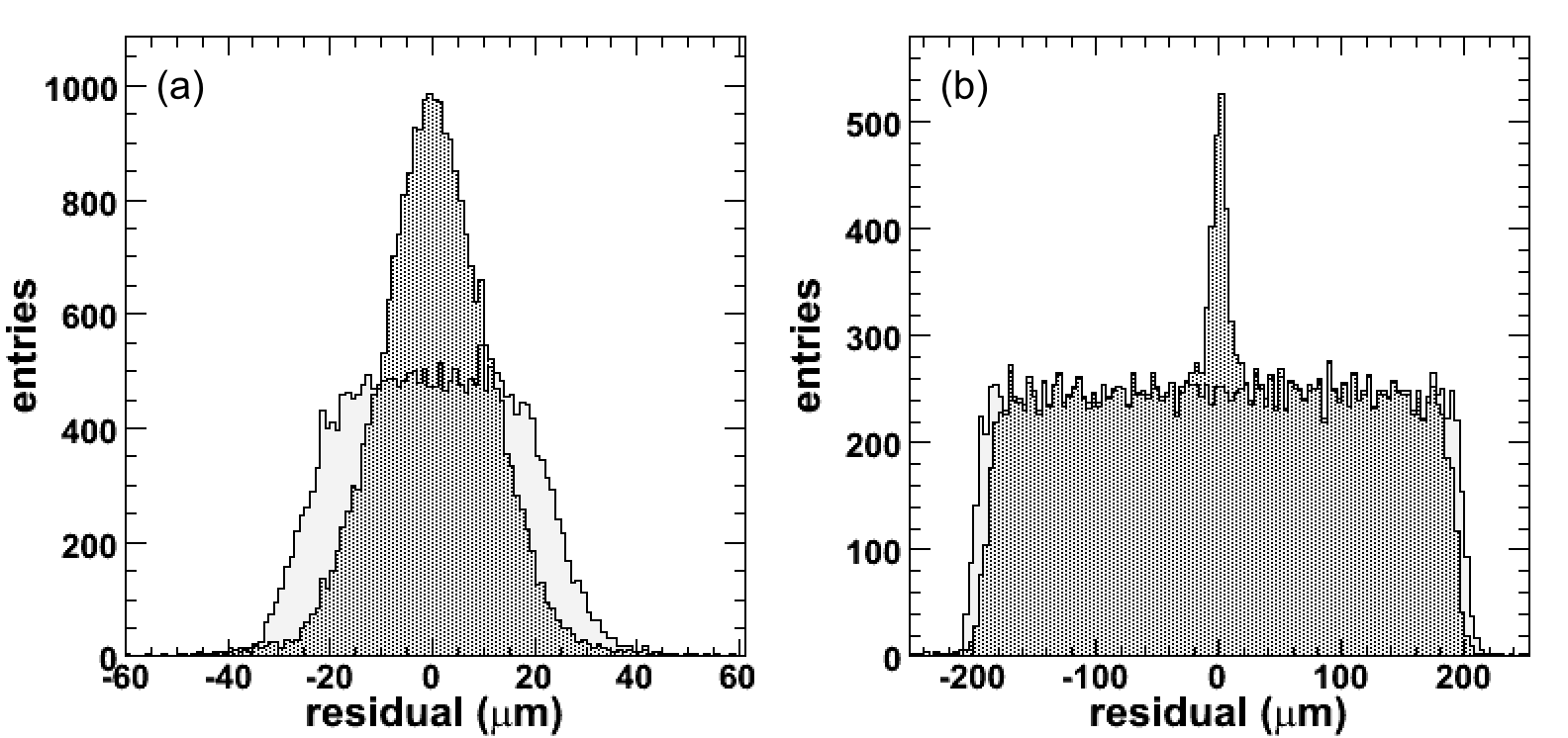
Finally, the spatial resolution is measured by plotting in Fig. 8 the difference between the track position predicted by the telescope on the plane of the DUT (the scCVD sensor) and the reconstructed hit of the DUT device. Figure 8 shows this distribution for both directions of the pixel. For the hit reconstruction first only the digital information is used (light gray distribution), i.e. the pixel with the largest charge signal above threshold collected in a cone around the extrapolated track position is taken as the hit pixel and its center is assumed to be the reconstructed position. The expected digital resolutions of pixel pitch divided by in both directions, i.e. 14.4 m and 115.5 m, respectively, folded by the resolution of the track extrapolation of about 5m, is observed. Position reconstruction which exploits the analog information available via the ToT readout is done by using the -algorithm [19]. This algorithm provides an improved resolution for clusters with more than one hit, especially double-hit clusters. Single-hit clusters effectively give binary response using . The corresponding residual distribution is shown by the dark histograms in fig. 8. It shows a pronounced peak with good resolution for clusters with two pixel hits, for which the -algorithm improves the resolution substantially. In the short pixel direction (Fig.8(a)), where the fraction of two hit clusters is about 40 the intrinsic resolution of the device, after quadratically subtracting the telescope extrapolation error of 5 m, becomes (8.9 0.1) m for a bias voltage of 200 V. The error quoted is obtained from the fit to the residual distribution. Systematic errors are not included as their exact determination turned out to be difficult, involving spatial S/N variations, alignment precision and its variation, as well as data sample (i.e. time/run) dependencies. From repeated analysis of several data samples, we conclude that an additional uncertainty in the order of 0.5 m has to be assumed.
Selecting events with two hit clusters only improves the resolution to 5m, telescope resolution quadratically subtracted, with the same uncertainty as quoted above. In the direction of the long pixel dimension (Fig.8(b)), the resolution for events with two-hit clusters (10) is an order of magnitude better than for events with single hit clusters.
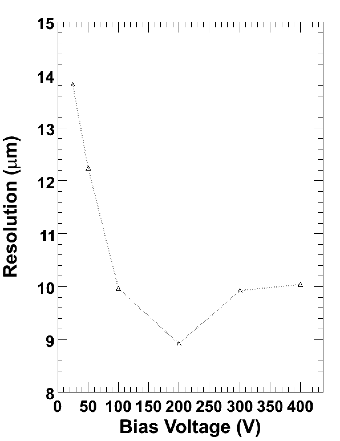
Figure 9 shows that the space resolution depends on the bias voltage. The charge collection efficiency and hence the total collected charge are field dependent until full charge collection is obtained. Also the sharing of charge between pixels due to diffusion depends on the field inside the sensor. The measured resolution shows an optimum between both effects at bias voltages of 200 V (fig. 9). The contribution of the telescope resolution is again subtracted in this figure. The uncertainty on the resolution measurements is in the order of 0.1m.
5 Conclusions
A single crystal chemical vapor deposition (scCVD) diamond sensor has been assembled as a hybrid pixel detector by using bumping and flip-chip technology with the ATLAS pixel readout chip FE-I3. As a pixel detector, scCVD diamond has been characterized for high energy particle detection for the first time. A high energy (100 GeV) pion test beam with a 4-plane microstrip beam telescope as a reference system has been used. The detector properties of scCVD diamond are free of effects observed previously with poly-crystalline (pCVD) devices: full charge collection over the sensor thickness (400m) for bias voltages above 100V (E=0.25V/m) is observed, no evidence for charge trapping and polarization fields is seen. The observed signal charge is 13000 e-. The operation of the device is characterized by low noise values (130 e-) and low threshold (1700 e-) settings. The measured charge distribution is a narrow Landau distribution due to the high density of the material. Hit detection efficiencies larger than 99.9 have been measured. The spatial resolution, obtained by using the digital hit information is consistent with that expected for a binary resolution. Exploiting charge sharing in the short pixel direction yields a measured intrinsic resolution of (8.9 0.1) m.
Acknowledgments
The authors would like to thank the CERN SPS staff for their help during data taking.
References
- [1] ATLAS Collaboration, G. Aad et al. The ATLAS Experiment at the CERN Large Hadron Collider. JINST 3 S08003, 2008.
- [2] CMS Collaboration, S. Chatrchyan et al. The CMS Experiment at the CERN Large Hadron Collider. JINST 3 S08004, 2008.
- [3] G. Aad et al. ATLAS pixel detector electronics and sensors. JINST 3 P07007, 2008.
- [4] H.C. Kastli et al. CMS barrel pixel detector overview. Nucl. Inst. and Meth., A 582:724–727.
- [5] M. Barbero et al. Development of Diamond Tracking Detectors for High Luminosity Experiments at the LHC. CERN LHCC-Report CERN/LHCC 2008-005, LHCC-RD-016, 2008.
- [6] W. Adam et al. Radiation hard diamond sensors for future tracking applications. Nucl. Inst. and Meth., A565:278–283, 2006.
- [7] M. Barbero et al. Development of Diamond Tracking Detectors for High Luminosity Experiments at the LHC. CERN LHCC-Report CERN/LHCC 2007-002, LHCC-RD-012, 2007.
- [8] W. Adam et al. RD42 Collaboration. The first bump bonded pixel detectors on CVD diamond. Nucl. Inst. and Meth., A 436:326–335.
- [9] J. Isberg et al. Science, 297:1670, 2002.
- [10] J. Wolf, G. Chmiel, and H. Reichl. Lead/Tin (95/5) solder bumps for flip chip applications based on Ti:W(N)/Au/Cu underbump metallization. In Proc. 5th Intl. TAB/Advanced Packaging Symposium ITAP, pages 141–152, San Jose, USA, 1993.
- [11] J. Wolf. PbSn60 solder bumping by electroplating. In Pixel 2000 Conference, Genova, Italy, June 2000. http://www.ge.infn.it/Pix2000/slides.html.
- [12] I. Peric, L. Blanquart, G. Comes, P. Denes, K. Einsweiler, P. Fischer, E. Mandelli, and G. Meddeler. The FEI3 readout chip for the ATLAS pixel detector. Nucl. Inst. and Meth., A565:178–187, 2006.
- [13] J. Treis, P. Fischer, H. Krüger, L. Klingbeil, T. Lari, and N. Wermes. A Modular PC Based Silicon Microstrip Beam Telescope with High Speed Data Acquisition. Nucl. Inst. and Meth., A490:112–123, 2002.
- [14] J. Fink, P. Lodomez, H. Kruger, H. Pernegger, P. Weilhammer, and N. Wermes. TCT characterization of different semiconductor materials for particle detection. Nucl. Inst. and Meth., A565:227–233, 2006.
- [15] The Particle Data Group, C. Amsler et al. Review of particle physics. 667:1, 2008.
- [16] H. Bichsel. Straggling in thin silicon detectors. Rev. Mod. Phys., 60, No. 3:663–699, 1988.
- [17] T. Stockmanns. Multi-Chip-Modul-Entwicklung für den ATLAS-Pixeldetektor. PhD Thesis, Bonn University, Internal Report: BONN-IR-2004-12, 2004.
- [18] T. Lari, A. Oh, N. Wermes, H. Kagan, M. Keil, and W. Trischuk. Charge collection properties in CVD diamond sensors. Nucl. Inst. and Meth., A537:581–593, 2005.
- [19] E. Belau et al. Nucl. Inst. and Meth., A 214:253, 1983.