Electrical detection of spin pumping: dc voltage generated by ferromagnetic resonance at ferromagnet/nonmagnet contact
Abstract
We describe electrical detection of spin pumping in metallic nanostructures. In the spin pumping effect, a precessing ferromagnet attached to a normal-metal acts as a pump of spin-polarized current, giving rise to a spin accumulation. The resulting spin accumulation induces a backflow of spin current into the ferromagnet and generates a dc voltage due to the spin dependent conductivities of the ferromagnet. The magnitude of such voltage is proportional to the spin-relaxation properties of the normal-metal. By using platinum as a contact material we observe, in agreement with theory, that the voltage is significantly reduced as compared to the case when aluminum was used.
Furtheremore, the effects of rectification between the circulating rf currents and the magnetization precession of the ferromagnet are examined. Most significantly, we show that using an improved layout device geometry these effects can be minimized.
pacs:
72.25.Ba, 72.25.Hg, 73.23.-b, 85.75.-dI Introduction
During the last several years there has been a continuing interest in high frequency phenomena in spintronic devices, as they are expected both to provide applications for microwave signal-processing, and to become a powerful new tool for fundamental studies of spin dynamics in magnetic nanostructures Slonczewski (1996); Berger (1996); Kiselev et al. (2003); Tulapurkar et al. (2005); Sankey et al. (2006).
It was predicted by Slonczewski Slonczewski (1996) and Berger Berger (1996) that angular momentum is transferred from spin polarized currents to the magnetization of the ferromagnets when charge currents are sent trough spin valves with non-collinear magnetizations (i.e. spin torque effect). This can excite and even switch the magnetization direction of the softer ferromagnet. Experiments with pillar-type structures Katine et al. (2000); Grollier et al. (2001); Sun (2000) confirmed these predictions.
It is natural to expect that if a spin current can induce magnetization motion the reciprocal process may also be possible: a moving magnetization in a ferromagnet can emit a spin current into an adjacent conductor. This effect is the so-called spin pumping, proposed by Tserkovnyak et al. (2002) and Brataas et al. (2002). Spin pumping is a mechanism where a pure spin current, which does not involve net charge currents, is emitted at the interface between a ferromagnet with a precessing magnetization and a normal-metal region. It is an important mechanism to generate spin currents, since other electronic methods based on driving an electrical current through a ferromagnet/semiconductor interface are strongly limited by the so-called conductance mismatch Schmidt et al. (2000). Berger Berger (1999) proposed a similar mechanism to generate a dc voltage by ferromagnetic resonance (FMR), based on spin-flip scattering in the ferromagnet as induced by spin waves.
Recently, spin pumping has been demonstrated in ferromagnetic resonance experiments with thin multilayers, where it appears as an enhancement of the Gilbert damping constant of magnetization dynamics Miz ; Urban et al. (2001); Heinrich et al. (2003); Lenz et al. (2004); Taniguchi and Imamura (2007), and using time resolved magneto-optic Kerr effect Woltersdorf et al. (2007). Although these experiments are very important in providing evidence for the spin pumping mechanism, the detection technique can be viewed as an indirect method to measure the spin pumping effect. Several experimental methods have been proposed to electrically detect the spin pumping mechanism Azevedo et al. (2005); Saitoh et al. (2006). The general problem of these methods is the rectification effects at the ferromagnet/normal-metal contact, which can suppress or mimic the spin pumping signal Costache et al. (2006a); Gui et al. (2005); Yamaguchi et al. (2007). Thus, the identification of these spurious effects is crucial and represents one of the main themes of this paper.
In a recent paper, Costache et al. (2006b) we have demonstrated spin pumping with a single permalloy strip in an electronic device, in which it is directly detected as a dc voltage signal. In this paper, we describe additional experiments on spin pumping effect, designed explicitly to eliminate the rectification effects. We explain in more detail the theoretical prediction for the voltage, and we identify and quantify different contributions of the rectification effect. Importantly, we show that by using an appropriate device geometry, these effects can be minimized.
II Spin pumping effect
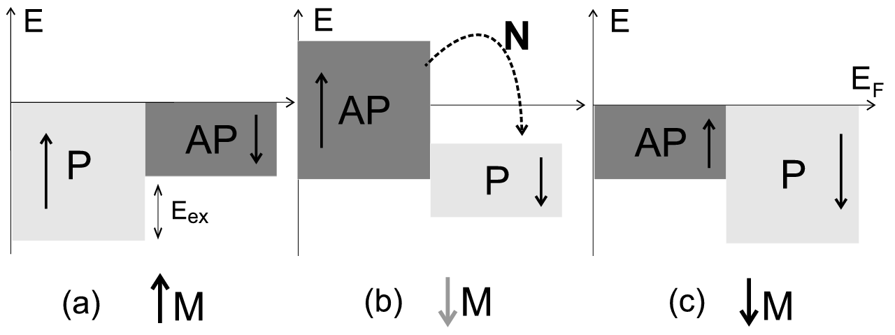
As discussed above, the emission of a spin current into a conductor by a moving magnetization of an adjacent ferromagnet is essentially the reciprocal of the spin torque mechanism in spin valves, where the magnetization is excited by a spin current.
A simplified picture of the process is schematically shown in Fig. 1. We consider a F/N junction at equilibrium, where in F exist a larger population of spins in the direction of magnetization, than antiparallel. When the magnetization direction is suddenly switched, the bands instantaneously shift in energy. However, in order to go back to the equilibrium situation there has to be spin transfer from one spin population to another (i.e. spin relaxation). If F is in contact with N, this transfer of spins can go via N. Thus the spin relaxation process for F is modified when it is in contact with an adjacent N, and depends on the spin relaxation properties on N. As a result, an ac spin current is emitted into N when the magnetization is switched back and forth under an oscillating magnetic field. Tserkovnyak et al. (2002) analyzed the case of circular precession of the magnetization and found that in addition to the ac current, a dc spin current is also emitted. A way to periodically change the magnetization direction is to put F into FMR, where circular precession of the magnetization can be resonantly excited by a small applied rf magnetic field Costache et al. (2006c, a).
The transfer of spin angular momentum by the precessing magnetization of F in contact with N (spin pumping) was first described Tserkovnyak et al. (2002) using the formalism of parametric charge pumping Bttiker et al. (1994) developed in the context of mesoscopic scattering problems. The main points of this description are discussed below.
Spin currents at the interface. As illustrated in Fig. 2, a spin current is pumped by the (resonant) precession of a ferromagnet magnetization into an adjacent normal-metal region. Assuming the F at FMR state, Tserkovnyak et al. (2002) have calculated the spin pumped current using a scattering matrix approach based on the microscopic details of the interface,
| (1) |
where m represents the magnetization direction. is the real part of the mixing conductance Hernando et al. (2000); Brataas et al. (2000), a material parameter which describes the transport of spins that are noncollinear to the magnetization direction at the interface and is proportional to the torque acting on the ferromagnet in the presence of a noncollinear spin accumulation in the normal metal Stiles and Zangwill (2002); Xia et al. (2002). This equation shows that the spin current, which goes into N, is perpendicular both to the magnetization direction m and to the change of m in time. This current has ac and dc components, but in the limit 1 (see later discussion), the time-averaged pumping current reads Brataas et al. (2002) .
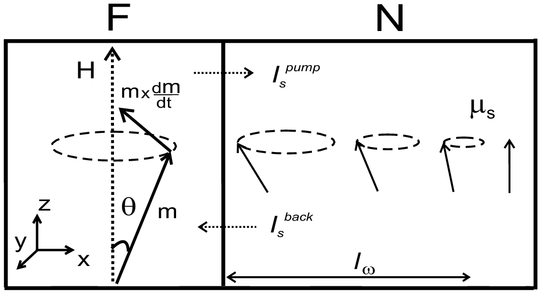
Depending on the spin related properties of the N, the spin current emission has two limiting regimes. When the N is a good “spin sink” (in which spins relax fast), the injected spin current is quickly dissipated and this corresponds to a loss of angular momentum and an increase in the effective Gilbert damping of the magnetization precession. This has been observed experimentally in nano-pillar structures Miz ; Urban et al. (2001); Heinrich et al. (2003); Lenz et al. (2004); Taniguchi and Imamura (2007). The total spin current is given by .
The opposite regime is when the spin-flip relaxation rate is smaller than the spin injection rate. In this case, a spin accumulation builds up in the normal metal (Fig. 2). The spin accumulation can diffuse away from the interface, but can also diffuse back into the F. This back flow current is given by
| (2) |
where is the one-spin density of states. The total spin current in this case is .
Spin battery. A spin battery operated by FMR has been proposed by the Brataas et al. (2002) in the limit of weak spin-flip scattering in the F. The spin accumulation in N can be calculated by solving the spin diffusion equation
| (3) |
where is the spin-flip time and is the diffusion coefficient in N. We assume that the spin diffusion length in N is much larger than the spin precession length ( is precessional frequency), i.e. , or equivalent by 1. This means that if the length of N is larger than , the x, y components of spin accumulation are fully averaged (due to dephasing) and the remaining z component is constant and along the static magnetic field direction Brataas et al. (2002). The time-averaged spin accumulation z in the N close to the interface readsBrataas et al. (2002)
| (4) |
where is the precession cone angle and is a reduction factor determined by the ratio between injection time and spin-flip relaxation time.
Intuitively, the spin accumulation can be measured electrically using a second ferromagnet as a spin dependent contact, placed at a shorter distance compared to the spin-flip length Jedema et al. (2002); Kimura et al. (2004); Valenzuela et al. (2005); Brataas et al. (2002).
Voltage at F/N interface. Importantly, Wang et al. (2006) have predicted a more direct way to detect the spin pump effect in which the precessing ferromagnet acts also as the detector. We have to take into account that the spin accumulation in a diffusive metal drives the spin current back into the F. The component parallel to m can enter F. Moreover, since the interface and the bulk conductances of F are spin dependent, this can result in charge accumulation, close to the interface, and thereby a dc voltage across the interface. The chemical potential difference across the interface has been calculated by Wang et al. (2006) following the lines of the Brataas et al. (2002) model, but including the spin diffusion back into F and spin-relaxation in F. As mentioned above, the relevant length-scale for the averaging of the transverse (x, y) components of the spin current is . Therefore for a device with dimensions larger than the spin-up (down) effective conductances of the interface are composed of the interface conductances in series with a conductance of the bulk N over a length scale of . These relations are given by and the mixing conductance , where (A is the area of the interface). Polarization is also introduced.
In the limit of large spin-flip in F and the size of N and for small angle precession (), the chemical potential difference is given by Wang et al. (2006)
| (5) |
where () is the conductance of the bulk N (F) over a length scale of (). For a thorough review of the above discussion see ref.Wang et al. (2006).
Interface currents matching. In this section, we describe a simple way to find the voltage (similar to Eq. 5) using spin-current matching at the interface. By writing all the currents involved in the process and matching them at the interface, all components of the spin accumulation at the interface can be determined. It is convenient to transform the equations into a rotating frame of reference in which the uniform magnetization motion can be formally eliminated, and the unit magnetization vector is . Basically, for this problem we have to consider three currents with their components. First, the spin pumping current (Eq. 1) is given by
| (6) |
Second, the back flow current consists of components parallel and perpendicular to , and can be written in terms of spin accumulation at the interface,
| (7) |
The sum of Eqs. 6 and 7, gives the total spin current on the F side of the interface. Third, the spin current on the N side of the interface is found by solving the Bloch equations for the spin accumulation in N, from this the current at the interface is given by Watts et al. (2006)
| (8) |
in terms of at the interface. This current has three components. The z component is determined only by the usual spin relaxation process. For the x and y components, two effects are important: precession, which results in mixing of the two components, depending on the time spent in N; and averaging, which reduces the total amplitude of the components. The spin accumulation is determined by matching the currents at the interface . The dc voltage at the interface is proportional to the projection of onto , and for the limit is given by
| (9) |
The simple form of Eq. 9 results from the relative independence of the dc voltage on (physical argument of this result remains to be clarified). For our devices (N = Al and F = Py). Using m-1, m-1, nm, nm and nm we estimate the conductances at room temperature:
| (10) |
And according to Xia et al. (2001), m-2. For a quantitative assessment of the relations 5 and 9 we assume () and (eV). First Eq. 9, by using we find dc voltage 20 nV. Second Eq. 5, by using , m-2 and m-2 (from ref. Jedema (2002)), the dc voltage is of the same order of magnitude 20 nV.
III Experimental Procedures
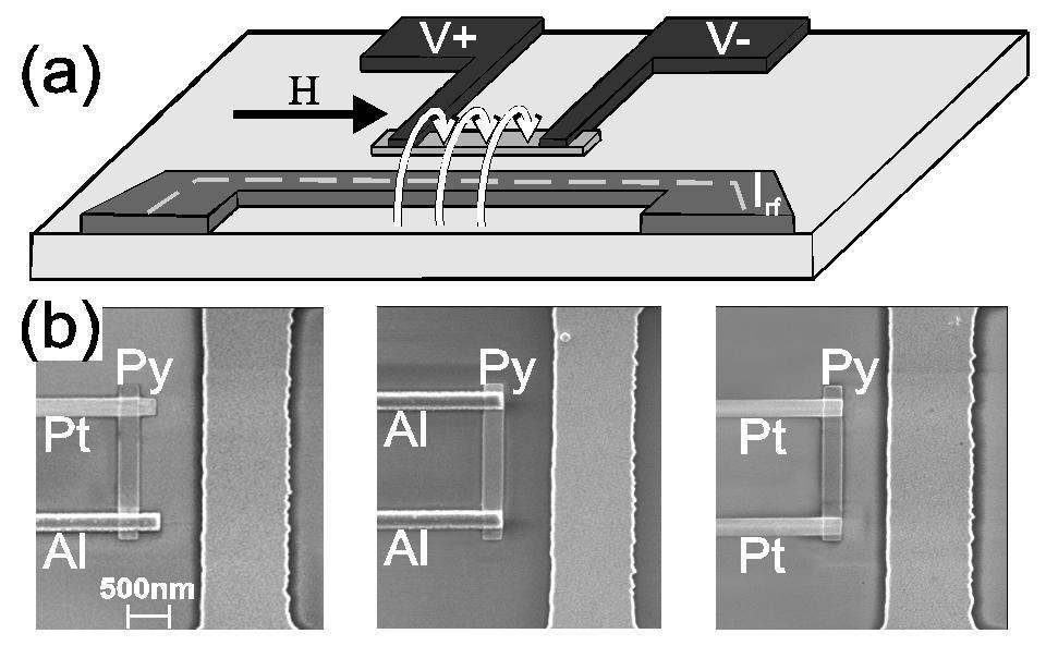
Our detection technique is based on the asymmetry in the spin pumping effect between two contacts in a device geometry where a ferromagnet is contacted with two normal-metal electrodes. The largest such asymmetry is obtained when one of the metal electrodes is a spin sink such as Pt, for which we expect a negligible contribution, while the other has a small spin flip relaxation rate, such as Al. Therefore, we anticipate a net dc voltage across a Py strip contacted by Pt and Al electrodes when the ferromagnet is in resonance.
Additional, we studied control devices where the Py strip is contacted by the same material Pt and Al. For these devices we expected no signal because: (i) The voltages for identical interfaces are the same and their contribution to cancels. (ii) Pt has a very short spin diffusion length, resulting in a small spin accumulation, a small backflow and thus a lower signal.
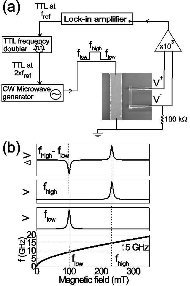
Figure 3(a) shows a schematic illustration of the lateral devices used in the present study. The central part of the device is a ferromagnetic strip of permalloy (Ni80Fe20, or Py) connected at both ends to normal metals, Al and/or Pt ( and contacts). The devices are fabricated on a Si/SiO2 substrate using e-beam lithography, material deposition and lift-off. A 25 nm thick Py strip with 0.33 lateral size was e-beam deposited in a base pressure of 1x mBar. Prior to deposition of the 30 nm thick Al or/and Pt contact layers, the Py surface was cleaned by Ar ion milling, using an acceleration voltage of 500 V with a current of 10 mA for 30 sec, removing the oxide and few nm of Py material to ensure transparent contacts. We measured in total 17 devices (this includes 4 devices with a modified contact geometry, described later in the paper). The different contact material configurations are shown in Fig. 3(b).
Figure 4(a) illustrates the experimental setup for the measurements. We measured the dc voltage generated between the , electrodes as a function of a slowly sweeping magnetic field () applied along the Py strip, while applying an rf magnetic field () perpendicular to the strip.
We have recently shown that a submicron Py strip can be driven into the uniform precession ferromagnetic resonance mode Costache et al. (2006c, a) by using a small perpendicular rf magnetic field created with an on-chip coplanar strip waveguide Gupta et al. (1996) (CSW) positioned close to Py strip (similar geometry as shown in Fig. 3). For the applied rf power 9 dBm, an rf current of passes through the shorted-end of the coplanar strip waveguide and creates an rf magnetic field with an amplitude of mT at the location of the Py strip cur . We confirmed with anisotropic magnetoresistance (AMR) measurements Costache et al. (2006a) that on-resonance the precession cone angle is .
In order to reduce the background (amplifier) dc offset and noise we adopted a lock-in microwave frequency modulation technique. During a measurement where the static magnetic field is swept from -400 mT to +400 mT, the rf field is periodically switched between two different frequencies and we measured the difference in dc voltage between the two frequencies using a lock-in amplifier. For all the measurements the lock-in frequency is 17 Hz and the difference between the two microwave frequencies is 5 GHz. A diagram of the measurement method is shown in Fig. 4(b).
IV Results and Discussion
IV.1 Detection of Spin pumping
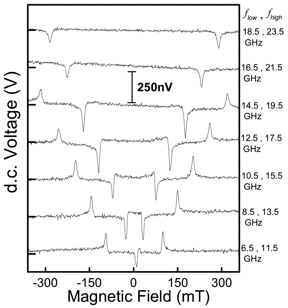
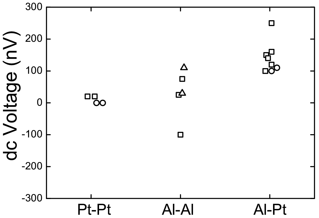
Here, we describe precise, room-temperature measurements of the dc voltage across a Py strip contacted by Pt and Al electrodes when the ferromagnet is in resonance. Figure 5 shows the electric potential difference from a Pt/Py/Al device. Sweeping the static magnetic field in a range -400 mT to +400 mT, a peak and a dip like signal are observed at both positive and negative values of the static field. Since we measured the difference between two frequencies, the peak corresponds to the high resonant frequency () and the dip to the low resonant frequency (), see Fig. 4(b). For the opposite sweep direction, the traces are mirror image. We measured 8 devices with contact material Pt/Py/Al. The measured resonances are all in the range +100 nV to +250 nV. Notably, the dc voltages are all of the same sign (always a peak for ), meaning that for Pt/Py/Al devices, the Al contact at resonance is always more negative than the Pt contact.
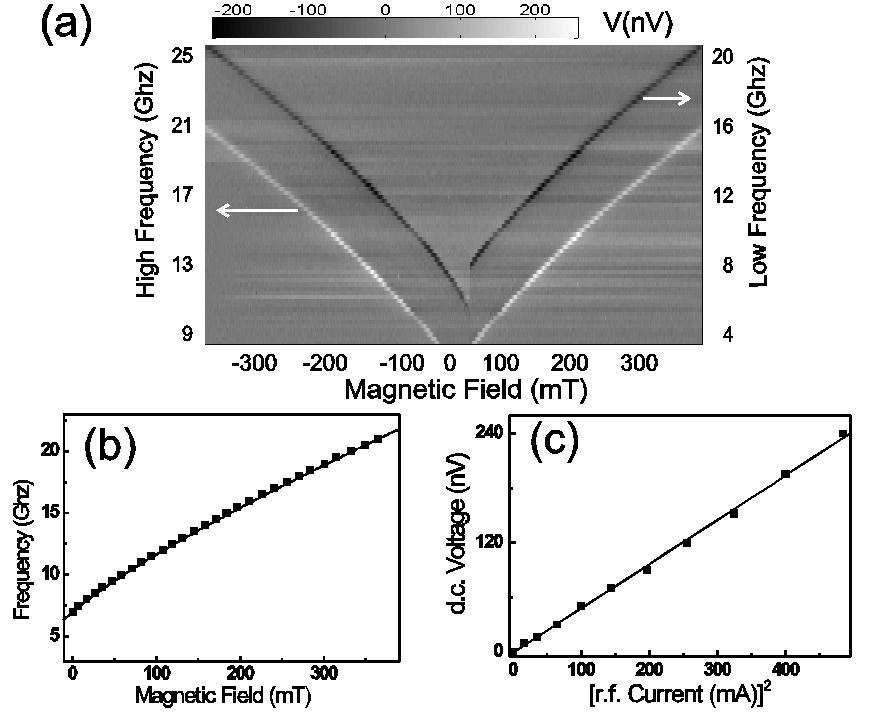
First, we look at the peak/dip position dependence of the rf frequency. In Figure 6(a), the dc voltage in gray scale is plotted versus static field for different high (low) frequencies of the rf field. Figure 6(b) shows the fitting of the peak/dip position dependence of the rf field frequency (dotted curve) using Kittel’s equation for a small angle precession of a thin-strip ferromagnet Kittel (1996):
| (11) |
where is the gyromagnetic ratio, , are in-plane (along the width of the strip) and out-of-plane demagnetization factors and is the saturation magnetization. The fit to this equation (see Fig. 6(b)) gives GHz/T, and mT, mT, consistent with earlier reports Giesen et al. (2005); Costache et al. (2006c). The fit confirms that the dc voltage appears at the uniform ferromagnetic resonance mode of the Py strip. The measured amplitude of the dc voltage as a function of the square of the applied rf current, at GHz and 139 mT is shown in Fig. 6(c). Here, we observe a linear dependence on the square of the rf current, consistent with the prediction of the spin pumping theory, see Eqs. 5 and 9.
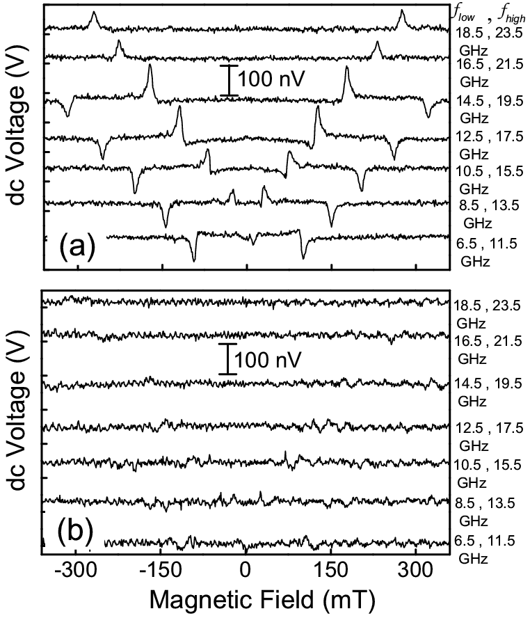
Further, we studied several control devices where both electrodes are of the same non-magnetic material, Al (5 devices) or Pt (4 devices). Here we expected no signal because of the reasons mentioned above. The results from Al/Py/Al devices show smaller signals than Pt/Py/Al devices, with a large scatter in amplitude and both with positive and negative sign for the resonance at . Values for the 5 devices are -100 nV (shown in Fig. 7(a)), +25 nV, +30 nV, +75 nV and +110 nV. In contrast, all 4 Pt/Py/Pt devices exhibit only weak signals less than 20 nV, with resonance signals barely visible, as in Fig. 7(b).
The overall values of the dc voltages as a function of different contact materials are shown in Fig. 8. We summarize the results as follow:
First, the Pt/Py/Al devices have signals that are always positive, on average , and with a scatter comparable in amplitude to that of Al/Py/Al devices around zero. This scatter in the signal amplitude can be due to: (i) samples variation, due to different interface quality, not identical contacts (i.e. different overlap between the N electrodes and the Py strip, see Fig. 3(b)) and a small variation in distance between the Py strip and the CSW; (ii) different rf power at the end of CSW, due to different positions and contact resistance of the microwave probe on the CSW. These characteristics are difficult to estimate for each device.
Second, we attribute the signals from Al/Py/Al devices to the asymmetry of the two contacts, possibly caused by small variation of the interfaces and in the contact geometry. Depending on the asymmetry, the signals therefore have a scatter around zero.
Third, in the Pt/Py/Pt devices, independent of possible asymmetry, we expected and found very small signals. Therefore, we conclude that the signals measured with the Pt/Py/Al devices arise mainly from the Al/Py interface.
IV.2 Spin pumping vs. Rectification effects
We now discuss the rectification effects. As we have shown recentlyCostache et al. (2006a), due to capacitive and inductive coupling between the CSW and the Py strip, rf currents () can be induced in the detection circuit. The rf currents in combination with a time-dependent AMR ()) can give a dc effect due to rectification effect (). However, for rectification to occur, the resistance must have first harmonic components, which is not true assuming circular or even elliptical precession of the magnetization.
There are two ways to have first harmonic components: (i) an offset angle between the applied field and the long axis of the Py strip, namely bulk rectification effect; (ii) an offset angle between the circulating rf currents and the magnetization. When the rf circulating currents enter and leave the strip, they can pass through a large angle relative to the magnetization. Asymmetry in the entry and exit paths, due to different conductivities of the two contacts, in combination with the time-dependent AMR, can lead to a rectification effect at the contacts, which we call the contact rectification effect Costache (2007).
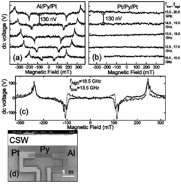
Even if, we can accurately control the offset angle between the applied field and the Py strip, we cannot rule out the contacts effect that may also contribute to the data presented in the previous section, see Fig. 5. A small contribution from rectification effects on top of spin pumping signal can also explain the asymmetric peak/dip shape which does not have a Lorentzian shape as expected from Eq. 5. In order to study these effects we prepared a new set of 4 devices very similar to the one shown in Fig. 3(b), but now with contacts at the ends of the Py strip, extending along the long axis of the strip, see Fig. 9(d) for a SEM image. In this geometry, the induced rf current flows through the contacts predominantly parallel to the magnetization direction. This suppresses the possible contribution to the measured dc voltages from a rectification effect at the contacts rec .
We first align the devices with Py strip parallel to the applied field and measure the dc voltage function of the field, as explained above. The measurements are shown in Fig. 9(a),(b) for Pt/Py/Al and a Pt/Py/Pt configuration. These results are consistent with the above discussion, as the Pt/Py/Al devices show signals equal to the average value measured in the previous device geometry, while the Pt/Py/Pt devices show no signal as expected. Figure 9(c) shows a comparison between the voltages of two Al/Py/Pt devices with longitudinal (bold line) and transverse (normal line) contacts geometry, at = 18.5 GHz, = 13.5 GHz. Particularly, devices with the longitudinal contacts exhibit, in addition to the main peak, a series of peaks at higher fields. An exact explanation of these observations is not yet clear. We assume these are related to end-mode resonances, since in this contacts geometry we are sensitive also to the magnetic structure of the ends of the Py strip. Moreover, we found no significant difference in the measured dc voltages between these two contacts geometries, Fig. 3(b) and Fig. 9(d).
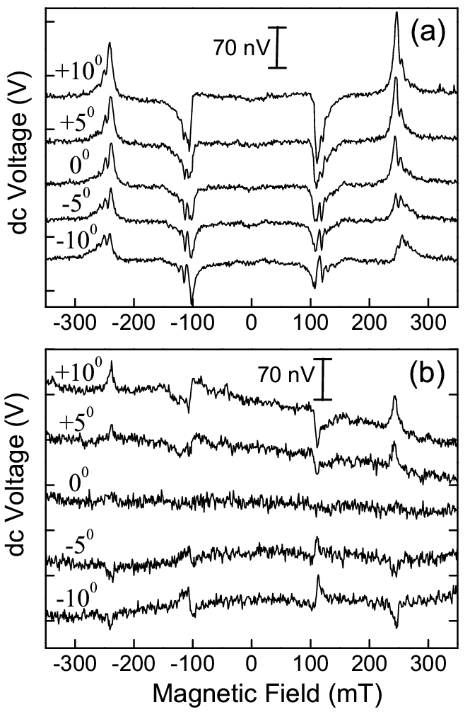
In order to confirm the above assumptions and to quantify the bulk rectification effect, we misaligned the direction of the static field with respect to the Py strip long axis by (and ) and measured the voltage at = 18 GHz, = 13 GHz. The results for Pt/Py/Al and Pt/Py/Pt devices are shown in Fig. 10. Note that we see significant contributions from the bulk rectification effect only at offset angles larger than . This rules out that small offset angles which may be present in the other geometry caused significant effects in the results, at most 10-20 nV.
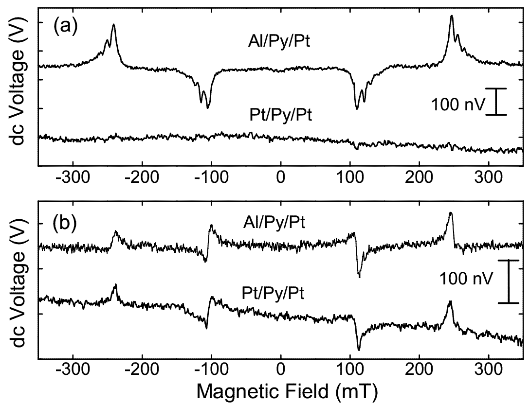
In the following, the above results are analyzed taking into account that the voltages measured in Pt/Py/Al devices are due to two effects: (i) spin pumping, and (ii) bulk rectification effect for a non-zero offset angle. Of these two effects only the bulk rectification depends on the sign of the offset angle. This means that if we take the sum of the voltages measured at , , we obtain two times the contribution from the spin pumping effect with a Lorentzian peak shape. And in contrast we expect no signal if we do the same operation for Pt/Py/Pt devices. These results are shown in Fig. 11(a).
On the other hand, if we subtract, , we obtain two times the contribution from the bulk rectification effect. Figure 11(b) shows the resulting data, which is practically the same for both devices, Pt/Py/Al and Pt/Py/Pt. Such a result is expected because the bulk rectification effect does not depend on the contact material.
We now consider a quantitative assessment of possible contribution to the measured
signal from rectification effects, namely bulk and contact rectification effect. Note, the contact rectification effect in principle should cancel for equivalent contacts. Both rectification effects depend primarily on the rf circulating current, which varies from device to device, depending on position of the pico-probe and rf current frequency. In a similar device geometry Costache
et al. (2006a) we have estimated the rf currents, to be up to 30 A. With this value we obtain:
(i) Bulk: A rough estimate of an upper bound contribution, assuming an offset angle of 2∘, gives 15 nV. The data shown in Fig. 10(b) (for zero degree) is less than this value.
(ii) Contact: This contribution, which is present only in devices with the transverse electrode geometry, is estimated at 30 nV Costache (2007).
The sum of these contributions can have any value between -45 and 45 nV, and thus can add or
subtract to the average spin pumping signal (150 nV), given the rise to extra scatter in the data, see Fig. 8.
In addition to signal magnitude analysis, it is also important to discuss the difference in signal shape due to these effects. It should be noted that each of the rectification effects discussed above can have a signal shape which can be any combination between absorptive and dispersive peak shape. In contrast, the spin pumping signal is only absorptive with a Lorentzian shape.
V Conclusion
We have presented dc voltage due to the spin pumping effect, across the interface between Al and Py at ferromagnetic resonance. We found that the devices where the Al contact has been replaced by Pt show a voltage close to zero, in good agreement with theory. We observed a quadratic dependence of dc voltage function of precession cone angle, in agreement with the discussed theory. Theoretical predicted spin pumping voltage (20 nV) is less than the values observed experimentally (in average 150 nV). This underestimation might arise from the fact that the model does not consider device geometry, disorder at the interface and assumes an homogeneous magnetization in the ferromagnet.
Furthermore, to rule out a possible contribution from rectification effects to the measured signal, we have studied devices with different electrode geometries. We observed that for a non-zero offset angle, between the static field and the Py strip, the measured voltages are due to two different effects, namely spin pumping and rectification effects. By using an appropriate device geometry, these effects can be quantified and for the zero offset angle the rectification effects are minimized.
This work demonstrates a means of directly converting magnetization dynamics of a single nanomagnet into an electrical signal which can open new opportunities for technological applications.
ACKNOWLEDGMENTS
We thank M. Sladkov, J. Grollier, A. Slachter, G. Visanescu, J. Jungmann for discussion and assistance in this project and B. Wolfs and S. Bakker for technical support. This work was supported by the Dutch Foundation for Fundamental Research on Matter (FOM), the Netherlands Organization for Scientific Research (NWO), the NanoNed and the DynaMax.
References
- Slonczewski (1996) J. C. Slonczewski, J. Mag. Magn. Mater. 159, L1 (1996).
- Berger (1996) L. Berger, Phys. Rev. B 54, 9353 (1996).
- Kiselev et al. (2003) S. I. Kiselev, J. C. Sankey, I. N. Krivorotov, N. C. Emley, R. J. Schoelkopf, R. A. Buhrman, and D. C. Ralph, Nature 425, 380 (2003).
- Tulapurkar et al. (2005) A. A. Tulapurkar, Y. Suzuki, A. Fukushima, H. Kubota, H. Maehara, K. Tsunekawa, D. D. Djayaprawira, N. Watanabe, , and S. Yuasa, Nature 438, 339 (2005).
- Sankey et al. (2006) J. C. Sankey, P. M. Braganca, A. G. F. Garcia, I. N. Krivorotov, R. A. Buhrman, and D. C. Ralph, Phys. Rev. Lett. 96, 227601 (2006).
- Katine et al. (2000) J. A. Katine, F. J. Albert, R. Buhrman, E. B. Myers, and D. C. Ralph, Phys. Rev. Lett. 84, 3149 (2000).
- Grollier et al. (2001) J. Grollier, V. Cros, A. Hamzic, J. M. George, H. Jaffr‘es, A. Fert, G. Faini, J. B. Youssef, and H. Legall, Appl. Phys. Lett. 78, 3663 (2001).
- Sun (2000) J. Z. Sun, Phys. Rev. B. 62, 570 (2000).
- Tserkovnyak et al. (2002) Y. Tserkovnyak, A. Brataas, and G. E. W. Bauer, Phys. Rev. Lett. 88, 117601 (2002).
- Brataas et al. (2002) A. Brataas, Y. Tserkovnyak, G. E. W. Bauer, and B. I. Halperin, Phys. Rev. B 66, 060404(R) (2002).
- Schmidt et al. (2000) G. Schmidt, D. Ferrand, L. W. Molenkamp, A. T. Filip, and B. J. van Wees, Phys. Rev. B 62, R4790 (2000).
- Berger (1999) L. Berger, Phys. Rev. B 59, 11465 (1999).
- (13) S. Mizukami, Y. Ando and T. Miyazaki, J. Magn. Magn. Mater. 226, 1640 (2001); Phys. Rev. B 66, 104413, (2002).
- Urban et al. (2001) R. Urban, G. Woltersdorf, and B. Heinrich, Phys. Rev. Lett. 87, 217204 (2001).
- Heinrich et al. (2003) B. Heinrich, Y. Tserkovnyak, G. Woltersdorf, A. Brataas, R. Urban, and G. E. W. Bauer, Phys. Rev. Lett. 90, 187601 (2003).
- Lenz et al. (2004) K. Lenz, T. Tolinski, J. Lindner, E. Kosubek, and K. Baberschke, Phys. Rev. B 69, 144422 (2004).
- Taniguchi and Imamura (2007) T. Taniguchi and H. Imamura, Phys. Rev. B 76, 092402 (2007).
- Woltersdorf et al. (2007) G. Woltersdorf, O. Mosendz, B. Heinrich, and C. H. Back, Phys. Rev. Lett. 99, 246603 (2007).
- Azevedo et al. (2005) A. Azevedo, L. H. L. O. Vilela, R. L. Rodriguez-Suarez, A. B. Oliveira, and S. M. Rezende, J. Appl. Phys. 97, 10C715 (2005).
- Saitoh et al. (2006) E. Saitoh, M. Ueda, H. Miyajima, and G. Tatara, Appl. Phys. Lett. 88, 182509 (2006).
- Costache et al. (2006a) M. V. Costache, S. Watts, M. Sladkov, C. H. van der Wal, and B. J. van Wees, Appl. Phys. Lett. 89, 232115 (2006a).
- Gui et al. (2005) Y. S. Gui, S. Holland, N. Mecking, and C. M. Hu, Phys. Rev. Lett. 95, 056807 (2005).
- Yamaguchi et al. (2007) A. Yamaguchi, H. Miyajima, T. Ono, Y. Suzuki, and S. Yuasa, Appl. Phys. Lett. 91, 132509 (2007).
- Costache et al. (2006b) M. V. Costache, M. Sladkov, S. M. Watts, C. H. van der Wal, and B. J. van Wees, Phys. Rev. Lett. 97, 216603 (2006b).
- (25) A. Brataas, International Conference on Nanoelectronics, Lancaster University, 4 - 9 January (2003).
- Costache et al. (2006c) M. V. Costache, M. Sladkov, C. H. van der Wal, and B. J. van Wees, Appl. Phys. Lett. 89, 192506 (2006c).
- Bttiker et al. (1994) M. Bttiker, H. Thomas, and A. Pretre, Z. Phys. B: Condens. Matter 94, 133 (1994).
- Hernando et al. (2000) D. H. Hernando, Y. V. Nazarov, A. Brataas, and G. E. W. Bauer, Phys. Rev. B 62, 5700 (2000).
- Brataas et al. (2000) A. Brataas, Y. V. Nazarov, and G. E. W. Bauer, Phys. Rev. Lett. 84, 2481 (2000).
- Stiles and Zangwill (2002) M. D. Stiles and A. Zangwill, Phys. Rev. B 66, 014407 (2002).
- Xia et al. (2002) K. Xia, P. J. Kelly, G. E. W. Bauer, A. Brataas, and I. Turek, Phys. Rev. B 65, 220401(R) (2002).
- Jedema et al. (2002) F. J. Jedema, H. B. Heersche, A. T. Filip, J. J. A. Baselmans, and B. J. van Wees, Nature 416, 713 (2002).
- Kimura et al. (2004) T. Kimura, J. Hamrle, Y. Otani, K. Tsukagoshi, and Y. Aoyagi, Appl. Phys. Lett. 85, 3501 (2004).
- Valenzuela et al. (2005) S. O. Valenzuela, D. J. Monsma, C. M. Marcus, V. Narayanamurti, and M. Tinkham, Phys. Rev. Lett. 94, 196601 (2005).
- Wang et al. (2006) X. Wang, G. E. W. Bauer, B. J. van Wees, A. Brataas, and Y. Tserkovnyak, Phys. Rev. Lett. 97, 216602 (2006).
- Watts et al. (2006) S. M. Watts, J. Grollier, C. H. van der Wal, and B. J. van Wees, Phys. Rev. Lett. 96, 077201 (2006).
- Xia et al. (2001) K. Xia, P. J. Kelly, G. E. W. Bauer, I. Turek, J. Kudrnovsky, and V. Drchal, Phys. Rev. B 63, 064407 (2001).
- Jedema (2002) F. J. Jedema, Ph.D. thesis, University of Groningen (2002).
- Gupta et al. (1996) K. C. Gupta, R. Garg, I. Bahl, and P. Bhartia, Microstrip Lines and Slotlines (Arttech House, Inc., Norwood, MA, 1996).
- (40) The 9 dBm applied rf power was converted into a rf current assuming load impedance.
- (41) The irregular feature, only occurring near mT is due to magnetization switching with hysteresis.
- Kittel (1996) C. Kittel, Introduction to Solid State Physics, Ch. 16 (John Wiley Sons, New-York, 7th ed., 1996).
- Giesen et al. (2005) F. Giesen, J. Podbielski, T. Korn, M. Steiner, A. van Staa, and D. Grundler, Appl. Phys. Lett. 86, 112510 (2005).
- Costache (2007) M. V. Costache, Ph.D. thesis, University of Groningen (2007).
- (45) Giving the arguments discussed, it is also posible a contribution from the rf currents flow in/out of plane. We have calculated this contribution and find that is negligible.