Resonant-tunnelling-assisted crossing for subwavelength plasmonic slot waveguides
Sanshui Xiao and Niels Asger Mortensen
DTU Fotonik - Department of Optics Engineering,
Technical University of Denmark, DK-2800 Kongens Lyngby, Denmark.
saxi@fotonik.dtu.dk
Abstract
We theoretically investigate the properties of crossing for two perpendicular subwavelength plasmonic slot waveguides. We show that, when encountering nano intersection, the crosstalk for the direct crossing is around , almost same as throughout. In terms of symmetry considerations and resonant-tunnelling effect, we design compact cavity-based structures. Our results show that the crosstalk is eliminated and the throughput reaches the unity on resonance. Simulations results are in agreement with those from the coupled-model theory. When taking into account of the material loss, due to the unchanged symmetry properties of the modes, the crosstalk is still suppressed. Our results may open a way to construct nanoscale crossings for high-density nanoplasmonic integration circuits.
OCIS codes: (240.6680) Surface plasmons; (130.2790) Guided waves; (130.3120) Integrated optics devices.
References and links
- [1] M. Lipson, “Guiding, modulating, and emitting light on Silicon - Challeges and opportunities,” J. Lightwave Technol. 23, 4222–4238 (2005).
- [2] W. Bogaerts, R. Baets, P. Dumon, V. Wiaux, S. Beckx, D. Taillaert, B. Luyssaert, J. Van Campenhout, P. Bienstman, and D. Van Thourhout, “Nanophotonic waveguides in silicon-on-insulator fabricated with CMOS technology,” J. Lightwave Technol. 23, 401–412 (2005).
- [3] T. Tsuchizawa, K. Yamada, H. Fukuda, T. Watanabe, J. Takahashi, M. Takahashi, T. Shoji, E. Tamechika, S. Itabashi, and H. Morita, “Microphotonics Devices Based on Silicon Microfabrication Technology,” IEEE J. Sel. Top. Quantum Electron 11, 232–240 (2005).
- [4] J. Takahara, S. Yamagishi, H. Taki, A. Morimoto, and T. Kobayashi, “Guiding of a one-dimensional optical beam with nanometer diameter,” Opt. Lett. 22, 475–477 (1997).
- [5] T. W. Ebbesen, C. Genet, and S. I. Bozhebolnyi, “Surface-plasmon circuitry,” Phys. Today 61, 44–50 (2008).
- [6] S. A. Maier, P. G. Kik, H. A. Atwater, S. Meltzer, E. Harel, B. E. Koel, and A. A. G. Requicha, “Local detection of electromagnetic energy transport below the diffraction limit in metal nanoparticle plasmon waveguides,” Nat. Mater. 2, 229–232 (2003).
- [7] K. Tanaka and M. Tanaka, “Simulations of nanometric optical circuits based on surface plasmon polariton gap waveguide,” Opt. Lett. 82, 1158–1160 (2003).
- [8] G. Veronis and S. Fan, “Guided subwavelength plasmonic mode supported by a slot in a thin metal film,” Opt. Lett. 30, 3359–3361 (2005).
- [9] L. Liu, Z. Han, and S. He, “Novel surface plasmon waveguide for high integration,” Opt. Express 13, 6645–6650 (2005).
- [10] D. F. P. Pile, T. Ogawa, D. K. Gramotven, Y. Matsuzaki, K. C. Vernon, T. Yamaguchi, K. Okamoto, M. Haraguchi, and M. Fukui, “Two-dimensionallly localized modes of a nanoscale gap plasmon waveguide,” Appl. Phys. Lett. 87, 261114 (2005).
- [11] S. I. Bozhevolnyi, V. S. Volkov, E. Devaux, J. Y. Laluet, and T. W. Ebbesen, “Channel plasmon subwavelength waveguide components including interferometers and ring resonators,” Nature 440, 508–511 (2006).
- [12] R. Zia, M. D. Selker, P. B. Catrysse, and M. L. Brongersma, “Geometries and materials for subwavelength surface plasmon modes,” J. Opt. Soc. Am. A 21, 2442–2446 (2004).
- [13] W. Bogaerts, P. Dumon, D. V. Thourhout, and R. Baets, “Low-loss, low-cross-talk crossings for silicon-on-insulator nanophotonic waveguides,” Opt. Lett. 32, 2801–2803 (2007).
- [14] T. Fukazawa, T. Hirano, F. Ohno, and T. Baba, “Low loss intersection of Si photonic wire waveguides,” Jpn. J. Appl. Phys. Part 1 43, 646–647 (2004).
- [15] H. Chen and A. W. Poon, “Low-loss multimode-interference-based crossings for silicon wire waveguides,” IEEE Photon. Technol. Lett. 18, 2260–2262 (2006).
- [16] D. Sarid, “Long-Range surface-plasma waves on very thin metal films,” Phys. Rev. Lett., 47, 1927–1930 (1981).
- [17] P. Berini, “Plasmon-polariton waves guided by thin lossy metal films of finite width: Bound modes of symmetric structures,” Phys. Rev. B, 61, 10484–10503 (2000).
- [18] J. Jung, T. Sondergaard, and S. I. Bozhevolnyi, “Theoretical analysis of square surface plasmon-polaritons waveguides for long-range polarization-independent waveguiding,” Phys. Rev. B, 76, 035434 (2007).
- [19] E. D. Palik, Handbook of Optical Constants of Solids (Academic, New York, 1985).
- [20] H. A. Haus, Waves and fields in optoelectronics (Prentice-Hall, Englewood Cliffs, N. J., 1984).
- [21] S. G. Johnson, C. Manolatou, S. H. Fan, P. R. Villeneuve, J. D. Joannopoulos, and H. A. Haus, “Elimination of cross talk in waveguide intersections,” Opt. Lett. 23, 1855–1857 (1998).
- [22] S. A. Marier, “Gain-assisted propagation of electromagnetic energy in subwavelength surface plasmon polariton gap waveguides,” Opt. Commun. 258, 295–299 (2006).
- [23] M. P. Nezhad. K. Tetz, and Y. Fainman, “Gain assisted propagation of surface plasmon polaritons on planar metallic waveguides,” Opt. Express 12, 4072–4079 (2006).
1 Introduction
It is of great interest for guiding light at deep subwavelength scales in optoelectronics, partly because it may enable ultra-density integration of optoelectronic circuits. Conventional dielectric waveguides cannot restrict the spatial localization of optical energy beyond the limit [1, 2, 3, 4], where is the free space photon wavelength and is the refractive index of the waveguide. Surface plasmon polaritons (SPPs) waveguides, which utilize the fact that light can be confined at metal-dielectric interface, have shown the potential to guide and manipulate light at deep subwavelength scales[5, 6, 7, 8, 9, 10, 11, 12]. The prospect of integration has motivated significantly recent activities in exploring plasmonic waveguide structures. In constructing highly dense integration of optoelectronic circuits, the ability to intersect waveguides is crucial owing to the desire for complex systems involving multiple waveguides. Usually, waveguide crossings require low intersection loss, low crosstalk, and compact dimensions. Several designs have been proposed for low-loss, low-crosstalk crossing of silicon-on-insulator nanophotonic waveguides [13, 14, 15]. However, to our knowledge, there are few studies about the waveguide crossings for SPP waveguides. Note that previously much attention has been focused on realizing the surface plasmon waveguide with long propagation length [16, 17, 18]. In this paper, we analysis the intersection loss of nanoplasmonic waveguide and design compact intersections with no crosstalk, based on resonant tunnelling effect. Results may open a way to construct nanoscale crossings for high-density nanoplasmonic integration circuits. Except for the dispersion of the SPP waveguide, the calculations mentioned below are performed by the finite-element method (FEM) in frequency domain.
2 Dispersion of surface plasmon polariton waveguide
Consider a subwavelength metal-dielectric-metal (MDM) constructed two-dimensional (2D) plasmonic waveguide. The propagation constant of surface plasmon polaritons can be obtained by solving the dispersion equation:
| (1) |
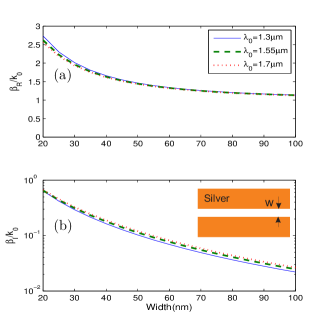
where and , the functions of , are the wave numbers of SPPs in dielectric and metal, respectively, and are the dielectric constants of the medium in guide region and metals, respectively, and is the width of the waveguide. For such a 2D plasmonic waveguide, the fundamental transverse magnetic mode () always exists even when the width is close to zero, while other high-order modes have a cutoff width. To satisfy single-mode condition, the width of the plasmonic waveguide should be smaller than , where is the mathematical arctangent function. For instance, the maximum width of the single-mode condition for the silver-air-silver SPP waveguide is about 720nm for . Figure 1 shows the dependence of of the fundamental SPP mode in 2D silver-air-silver waveguide on the width () of the waveguide and working wavelength of light in free space, where . From Fig. 1, one can see that the effective refractive index () of SPP mode is always larger than that of the dielectric medium, i. e., . The loss arisen from the intrinsic loss of the metal increases when shrinking the width of the plasmonic waveguide. In this paper, the waveguide width is chosen to be much smaller than the waveguide to have the single-mode property of the SPP waveguide.
3 Direct crossing for two perpendicular plasmonic waveguides
When considering the waveguide crossing, the confinement in the direction perpendicular to the wave propagation is lost near the crossing region, thus causing diffraction of the light. The diffraction strongly depends on size and the index-contrast of the waveguide. The loss for the waveguide crossing of low-index-contrast waveguides is negligible, while the mode diffracts dramatically for the nano-size of high-index-contrast waveguides. Previous studies show that the high-index-contrast systems, such as silicon-on-insulator nanowires with of 2.34 (), have a large intersection loss for the direct waveguide crossing. The silver-air-silver plasmonic waveguide studied here is a size of a few hundred nanometers, having a quite large index-contrast of 9.3() for the working wavelength 1.55 . One believes that the SPP mode will be significantly diffracted when passing through a waveguide crossing with nano size.
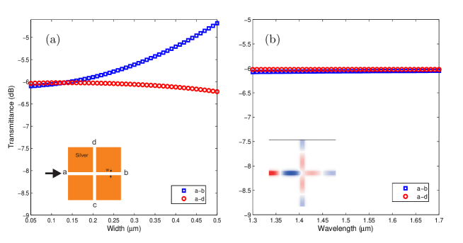
To clearly illustrate it, we first analysis the behavior of intersection loss for the direct waveguide crossing of nanoplasmonic waveguides, as shown in the inset of Fig. 2(a). Suppose an optical beam incident from port a. Obviously the beam diffracts when encountering the crossing region. The fraction power transmission are shown in Fig. 2. For simplicity, here we assume that the metal is lossless, i.e, neglecting the imaginary part of metal dielectric permittivity. Fig. 2 (a) shows the fraction power transmission as a function of the width of the plasmonic silver-air-silver waveguide for the working wavelength 1.55 , where denotes the width of the waveguide. The squares and circles represent the straightforward transmittance (a-b) and crosstalk (a-d), respectively. The straightforward transmittance drops down when the width of the plasmonic waveguide decreases from 500 to 50 , and the crosstalk slightly increases when decreasing the waveguide’s width. For the case of =200 , the straightforward throughout is about -5.89dB () and crosstalk is about -6.03dB (). From Fig. 2 (a), one concludes this kind of direct waveguide crossing has low transmission and high crosstalk. It is also interesting to note that, when encountering nano intersection, the throughout is around -6.00dB (), almost same as crosstalk. The transmittance spectra, for the case of =100 , with straightforward line (a-b) and crosstalk line (a-d) are shown in Fig. 2 (b). In all calculations mentioned in this paper, frequency-dependent dielectric function of the Silver is described by the lossy Drude model , where / is the relative permittivity at infinite/zero frequency, is the plasma frequency, and is the collision frequency. We choose , , and for the Drude model, which fits the experimental data [19] quite well. For the wavelength of our interests, the throughout keeps the same value of -6.00dB (), as well as the crosstalk. The inset of Fig. 2 (b) shows the profile of a steady-state magnetic field at the working wavelength 1.55 , which illustrates that the throughout is almost same as the crosstalk.
4 Resonant-tunnelling assisted transmittance for subwavelength plasmonic slot waveguide
To decrease the crosstalk and enhance the straightforward transmittance of the crossing waveguide intersection, one can aim to reduce the diffraction in the crossing region. In order to suppress effectively the diffraction, generally an intersection region with a large size of numbers of wavelength is used, which results in low packing density of optical circuits. In this paper, we utilize the well-known effect of resonant tunnelling through a cavity to eliminate the crosstalk and increase the straightforward transmittance. Firstly we consider a system consisting of a subwavelength silver-air-silver plasmonic waveguide coupled to a rectangular cavity, which supports a resonant mode of frequency . For such a system, the transmission can be described by the resonant tunnelling effect, and one can use the coupled-mode theory [20] to evaluate the power transmission and reflection on resonance by
| (2) | |||
| (3) |
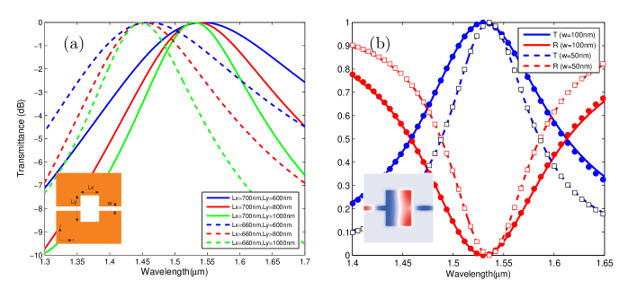
where is the decay rate due to the internal loss in the cavity and is the decay rate of the field in the cavity due to the power escape through the waveguide. From the above equations, one can see the direct relation between the transmittance/reflection and the ratio on resonance. If there is no internal loss in the cavity (), the incident wave is completely transmitted and the spectral width of the resonance is determined by the strength of the coupling between the waveguide and the cavity (). Consider a resonant system, shown in the inset of Fig. 3(a). To keep structural symmetry, the center of the cavity is placed at the center of the plasmonic waveguide and the side length of the rectangular cavity is denoted by . Assuming that the metal is lossless, the transmission coefficients of the device [inset of Fig. 3(a)] with different side length of the cavity are shown in Fig. 3(a), where the width of the plasmonic waveguide is fixed as 100 . From Fig. 3(a), we observe that the resonant frequency of the cavity strongly depends on the side length of the cavity in direction , while slightly shifts when varying . We also find out that, for a fixed value of , the quality factor () of the resonant system increases when enlarging . is around 5 when =700 , =600 , and increases to 10 for =700 , =1000 . Fig. 3(b) shows the transmission and reflection of the device (=700 , =1000 ) as a function of the wavelength for =50 and =100 , respectively. The solid and dashed lines in Fig. 3(b) represent the results from the FEM method, and the open squares and solid circles in Fig. 3(b) are obtained from the coupled-mode theory. Results from coupled-mode theory are in agreement with those from the FEM method. Since the metal is assumed to be lossless, there is no internal loss in the cavity and there is, therefore, complete transmission on resonance, as seen in Fig. 3(a) and Fig. 3(b). In this coupling system, the coupling strength can be tuned by the width of the plasmonic waveguide. Decreased the width results in a weaker coupling and, therefore, higher quality factor and narrower spectral width of the resonance. For the case of =100 , is about 10 and becomes 15 for =50 . For the lossless case, because of infinitive , is solely determined by the coupling strength , , . From Fig. 3(b), we also observe that the resonant frequency of the cavity slightly shifts when is varied. The inset of Fig. 3 (b) shows the profile of a steady-state magnetic field at the resonant frequency for =100 , which illustrates the complete transmission on resonance. From the mode distribution in the rectangular cavity[inset of Fig. 3(b)], we can explain why the resonant frequency of the cavity is strongly dependent to , while almost independent to , as mentioned above.
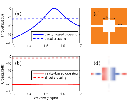
Next let us consider coupling of the four branches of the perpendicular intersection for two plasmonic waveguides in terms of a resonant cavity at the center, as shown in Fig. 4 (c). Based on symmetry considerations, when the resonant mode that is excited from the input port can be prevented from decaying into the transverse ports, the crosstalk can be prohibited and the system reduces to the resonant tunnelling phenomenon through a cavity. To achieve it, there are general criteria for perpendicular intersection of two waveguides, as mentioned in detail in Ref. [21]. To achieve it, the following conditions should be satisfied: (1) Waveguide: single-mode with mirror symmetry plane through its axis and perpendicular to the other one; (2) Cavity: symmetric with respect to the mirror planes of both waveguides; (3) Cavity modes: only two degenerate modes with different symmetry with respect to waveguide s mirror plane. When these requirements are satisfied, due to its orthogonality to the mode in the other waveguide, each resonant state can couple solely to the mode in just one waveguide, thus the crosstalk will be eliminated. From the mode profile [inset of Fig. 3 (b)], one can easily see that the resonant mode supported by the rectangular cavity is even with respect to one waveguide’s mirror plane and odd with respect to the other and that there is only one resonant mode in the wavelength range of interest in Fig. 3. In terms of the general criteria mentioned above, the crosstalk for the perpendicular intersection [Fig. 4 (c)] will be possibly inhibited when introducing a square cavity in the intersection. One also note that for the 2D case the bulk material (Silver) can prevent any radiation losses. Following this idea, we design quite a simple crossing intersection with a square resonant cavity, as shown in Fig. 4(c). Figs. 4 (a) and 4 (b) show the transmission spectra of the devices with direct crossing and cavity-based crossing (the solid line). Compared with the result for direct crossing (the dashed line), the throughput (solid lines) in Fig. 4 (a) is really enhanced due to the resonant-tunnelling effect and reached the unity on resonance. The crosstalk (the solid line) for cavity-assisted crossing, shown in Fig. 4(b), is almost prohibited relative to unmodified crossings. The crosstalk is close to zero in the whole frequency range of interest, which can be naturally understood by the general criteria mentioned above. Fig. 4 (d) shows of a steady-state magnetic field at the resonant frequency for =20 , which illustrates the energy is fully transmitted forward through the crossing section. We also note that the size of the intersection is quite compact, which is vital for high-density integration.
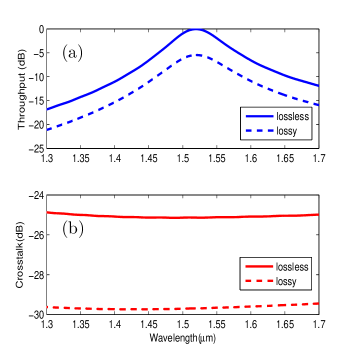
All calculations mentioned above are performed when ignoring the material loss. Note that the metal, Silver, is always a lossy material especially in the visible and infrared frequency region. This kind of loss usually limits the optical performance of the plasmonic devices. For the device studied here, the loss will result in large propagation loss of the plasmonic waveguide and low quality factor of the unloaded resonant plasmonic cavity. However, when we take into account of it, the symmetric properties of cavity modes will keep unchanged, as well as that for the waveguide mode. We believe that the general criteria for eliminating the crosstalk of the perpendicular intersection are still satisfied, i. e., the crosstalk can also be inhibited when taking into account of the material loss. From Eqs. (2)-(3), one knows that the spectrum will not reach unity on resonance. This is because the factor significantly decreases when considering the material loss and becomes comparable to . Here, we recalculate the transmission spectra for the perpendicular intersection [see Fig. 4 (c)] without ignoring the material loss, and results are shown in Fig. 5. Figs. 5 (a) and 5 (b) show the transmission spectra of the devices [see Fig. 4 (c), =680 , =20 ]. The solid and dashed lines represent the results when ignoring the material loss (the solid line) and considering the loss (the dashed line), respectively. When we take into account of the loss, the throughput shown in Fig. 5 (a) is only about -5.47dB on resonance, which is arisen from the propagation loss of the waveguide mode and the reflection by the plasmonic cavity. At telecommunication windows, around 1.5 , the SPP propagation length is greater than the total length of the circuit and can reach values close to 1 . The propagation loss can be possibly miniaturized for each plasmon device. Apart from the propagation loss, the intersection loss for the device [see Fig. 4 (c)]is about -0.27dB on resonance, which is limited by the value of . For the lossless case, the is around 20 and becomes 15 when considering the loss. of the unloaded cavity with the lossless case is much larger than , thus we can obtain . Due to the metal loss, strongly decreases. Assuming that the coupling strength are the same for both cases, one can obtain that becomes 60 for the lossy case. In order to improve the transmittance property, what we can do is to increase the value of . Recently, people use the gain material to annul the effect of material loss, thus improving the optical performance of loss-limited plasmonic devices[22, 23]. From Fig. 5(b), one can also observe that the crosstalk is also prohibited without ignoring the loss. The simulation results agree very well with what we expect in the analysis mentioned above.
5 Summary
In this paper, we analysis the intersection loss for two perpendicular plasmonic waveguides. For the direct crossing, when encountering nano intersection the throughout is around , almost same as crosstalk. Using a general recipe for elimination of crosstalk, we design simple cavity-based structures to enhance the throughput and eliminate the crosstalk. The size of the intersection is quite compact, which is vital for high-density integration. Numerical results are calculated by FEM in frequency domain, which agree well with those from the coupled-model theory. Without considering the material loss, the throughput reaches the unity on resonance and the crosstalk is suppressed, close to zero. Results can be explained in terms of symmetry considerations and resonant tunnelling effects. For the lossy case, due to the unchanged symmetry properties of the cavity modes and waveguide mode, the crosstalk is also suppressed and the throughput never reaches the unity on resonance. Apart from the propagation loss, the intersection loss for the device is about -0.27dB on resonance. Our results may open a way to construct nanoscale crossings for high-density nanoplasmonic integration circuits.
Acknowledgments
This work is financially supported by the Danish Research Council for Technology and Production Sciences (grants no: 274-07-0379, 274-07-0080) as well as the Danish Council for Strategic Research through the Strategic Program for Young Researchers (grant no: 2117-05-0037).