Intrinsic and extrinsic corrugation of monolayer graphene deposited on SiO2
Abstract
Using scanning tunneling microscopy (STM) in ultra high vacuum and atomic force microscopy, we investigate the corrugation of graphene flakes deposited by exfoliation on a Si/SiO2 (300 nm) surface. While the corrugation on SiO2 is long-range with a correlation length of about 25 nm, some of the graphene monolayers exhibit an additional corrugation with a preferential wave length of about 15 nm. A detailed analysis shows that the long range corrugation of the substrate is also visible on graphene, but with a reduced amplitude, leading to the conclusion that the graphene is partly freely suspended between hills of the substrate. Thus, the intrinsic rippling observed previously on artificially suspended graphene can exist as well, if graphene is deposited on SiO2.
pacs:
68.55.J-, 68.37.Ef, 68.37.Ps, 68.65.-kSince it was believed, based on the Mermin-Wagner theorem, that two-dimensional (2D) crystals are not stable at finite temperature Mermin (1968), it came as a surprise that monolayer graphene could be stabilized on a Si/SiO2 substrate Novoselov et al. (2004); Zhang et al. (2005); Geim and Novoselov (2007). Due to its peculiar properties like, e.g., a linear dispersion leading to Klein tunneling Katsnelson et al. (2006), high room-temperature mobility allowing quantum Hall steps at 300 K Novoselov et al. (2007), a low spin-orbit interaction beneficial for spintronic devices Tombros et al. (2007) or tunable spin-polarized edge states Son et al. (2006), graphene studies have become a major issue in solid-state physics. Already the first transport results not exhibiting weak localization lead to the speculation of a curved surface Morozov et al. (2006) acting as a phase-breaking field McCann et al. (2006). Such a curvature was indeed observed by microscopic electron diffraction of suspended monolayer graphene sheets Meyer et al. (2007). The lateral wavelength of the isotropic curvature is estimated to be nm with an amplitude of nm. The rippling has been reproduced theoretically by Monte-Carlo simulations with a preferential wavelength of 8 nm barely depending on temperature Fasolino et al. (2007). It is argued that the anharmonic coupling between bending and stretching modes in graphene causes the rippling and is responsible for the stability of the 2D crystal. Moreover, it has been shown experimentally that rippling can ultimately limit the mobility of graphene at 300 K, if defects are avoided Morozov et al. (2008)
However, the corrugation properties of graphene deposited on a substrate as typically used in transport experiments are not clarified. In particular, previous scanning probe studies Stolyarova et al. (2007); Ishigami et al. (2007); Tikhonenko et al. (2008); Zhang et al. (2008) revealed only corrugations, which are attributed to the roughness of the underlying substrate, except for a torn flake manipulated by AFM Tikhonenko et al. (2008). Thus, it is unclear, if the intrinsic tendency for rippling persists on the substrate, thereby ultimately limiting mobility and influencing weak localization, which has meanwhile been found, at least, for some samples Tikhonenko et al. (2008). Here, we demonstrate that a regular short wave-length corrugation with nm and nm, which is not induced by the substrate, can even prevail the substrate corrugation. Since and are close to the values found on suspended graphene Meyer et al. (2007), we attribute this additional corrugation to the intrinsic rippling of graphene Fasolino et al. (2007). Moreover, we find that the long-range corrugation implied by the substrate has lower amplitude on graphene than on SiO2 suggesting that our high-mobility graphene is partly suspended between hills of the substrate, which might favor the development of the intrinsic short-scale rippling.
The graphene sample is fabricated by the mechanical exfoliation technique as described in Novoselov et al. (2004); Lemme et al. (2007). Using an optical microscope, a graphene flake containing a monolayer region is identified. Raman spectroscopy is used to confirm the number of layers with the help of the 2D line Ferrari et al. (2006). Fig. 1(a) shows three spectra measured in different areas of the flake visible in Fig. 1(b). In addition to a large monolayer area, we find smaller bi- and multilayer areas as marked by 1L, 2L and MuL, respectively. Next, gold contacts with a 10 nm Cr seed layer were deposited and structured with a lift-off process. Except for one side, the graphene sample is completely surrounded by the gold electrode as shown in Fig. 1(b). The mobility of graphene samples prepared identically but with several contacts is m2/(Vs) at 300 K Lemme et al. (2008), i.e. comparable with high-mobility values obtained by other groups Morozov et al. (2008); Tan et al. (2007). In order to remove residual resist and adsorbates, the sample was rinsed in isopropanol and acetone, baked out to 150∘ C in air for four hours and, additionally, baked out to the same temperature in ultrahigh-vacuum (UHV) for three hours. The gold film served as the electrical contact for scanning tunneling microscopy (STM) and was used to prepare the STM tip (etched W) by voltage pulses. In order to find the graphene within the UHV-STM, we used an optical microscope with a focal length of 30 cm and 5 m lateral resolution. Fig. 1(c) shows a microscopic image of the tip approaching the graphene flake. The home-built STM features an stage for lateral positioning and operates in UHV ( Pa) as described elsewhere Wiebe et al. (2004); Geringer et al. . The stage has been checked to move accurately within 10 %. Topographic images are recorded applying a bias to the tip. Spectroscopic curves are measured by lock-in technique using a modulation voltage after stabilizing the tip at voltage and current . STM images obtained at the intentionally irregular edge of the gold contact are displayed in the insets of Fig. 1(b). They are used for orientation by STM and aid in finding monolayer, bilayer and multilayer areas on the flake.
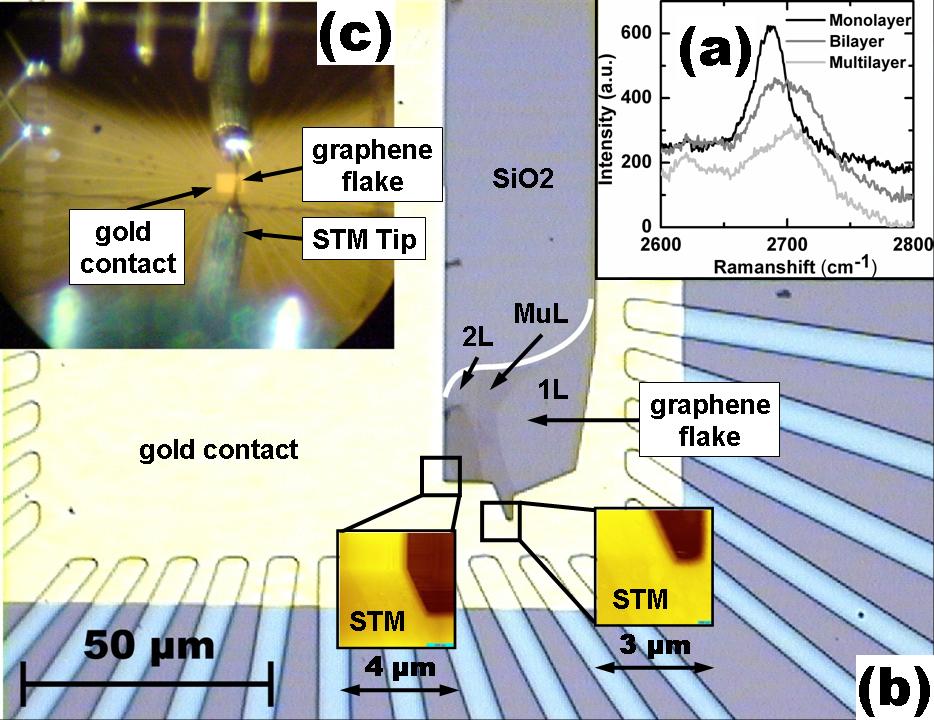
Atomic force microscopy images are taken under ambient conditions in tapping mode using either a commercial cantilever with a silicon tip or an ultrasharp tungsten tip with a tip radius of 1 nm, which is attached at the bottom of a Si cantilever can . Imaging has been carried out in the attractive regime Hölscher and Schwarz (2007) with an oscillation frequency slightly above resonance.
Fig. 2(b) and (c) show two atomically resolved STM images recorded on the monolayer (1L) and the multilayer (MuL) of graphene, respectively. One observes a hexagonal pattern on the monolayer and a triangular pattern on the multilayer in accordance with previous results Stolyarova et al. (2007); Zhang et al. (2008). The atomic resolution is still perceptible at lower resolution in Fig. 2(a) and (d), but an additional irregular corrugation appears. Line sections shown in Fig. 2(e) reveal that the corrugation height on this monolayer region is about 0.6 nm, a factor of three larger than on the multilayer region. Notice that corrugation heights pretended by charged defects are typically smaller by more than an order of magnitude Wittneven et al. (1998). A representative curve of the monolayer, which is known to represent the local density of states (LDOS) Stroscio et al. (1986), is shown in Fig. 2(f). As expected for graphene, it shows a V-like shape with the Dirac point at about mV. It does not change significantly across the area depicted in Fig. 2(d). Note that graphene on SiC(0001) exhibits a more complicated spectrum Brar et al. (2007); Rutter et al. (2007); Lauffer et al. (2008). Note also, that we did not observe the phonon gap found at 4 K recently Zhang et al. (2008), although we used several different micro- and macrotips. This is tentatively attributed to the different temperature of the two experiments. The good representation of the graphene LDOS by and the continuous atomic resolution across Fig. 2(d) demonstrates the absence of resist on this part of the surface. Indeed, we found several large areas without resist, but still also areas where a remaining resist is apparent within the STM images. The fact that the Dirac point is observed close to 0 V shows a negligible influence of charging adsorbates, which are probably removed in UHV.
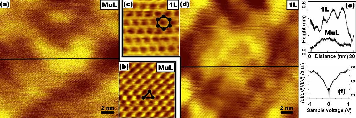
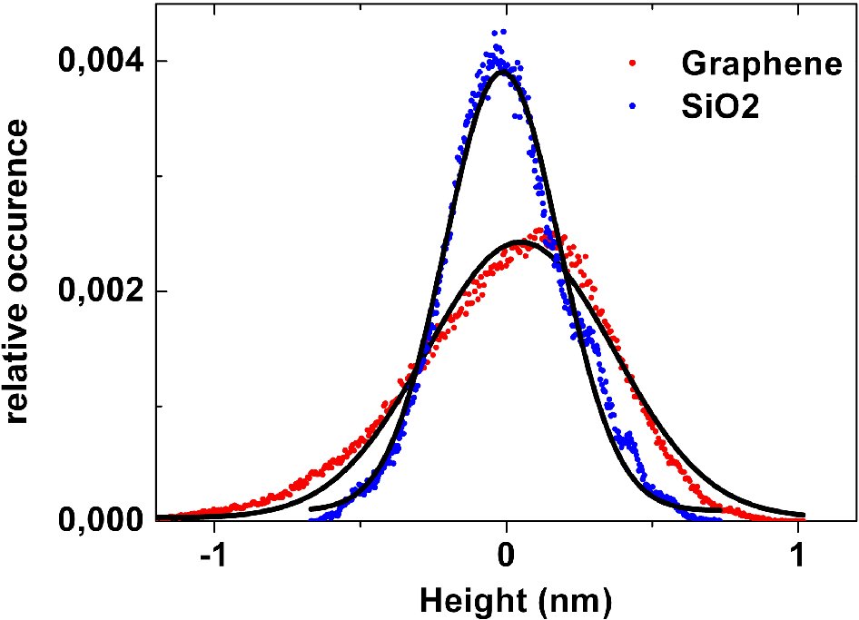
Fig. 3(a) shows a large area STM image of the graphene monolayer. One observes a rather regular corrugation with amplitudes of more than 1 nm and a preferential distance between hills of about 15 nm. The histogram EPAPS is Gaussian with a full width at half maximum (FWHM) of 0.78 nm. The rms roughness is determined to be 0.36 nm. The latter two values fluctuate across the monolayer area by about 25 % (average rms roughness 0.32 nm), but the corrugation length scale remains constant. For comparison, Fig. 3(c) shows an AFM image of the bare SiO2 surface recorded in tapping-mode. It is obvious that the corrugation on the substrate is lower and exhibits a larger length scale than the corrugation on graphene. The FWHM of the histogram of Fig. 3(c) is 0.48 nm and the rms roughness is 0.22 nm (average of all data nm). We used four different tips, including two ultrasharp tips with a tip radius of 1 nm can , but always observed the same corrugation height and length scale, which, in addition, is in good agreement with previous results Ishigami et al. (2007).

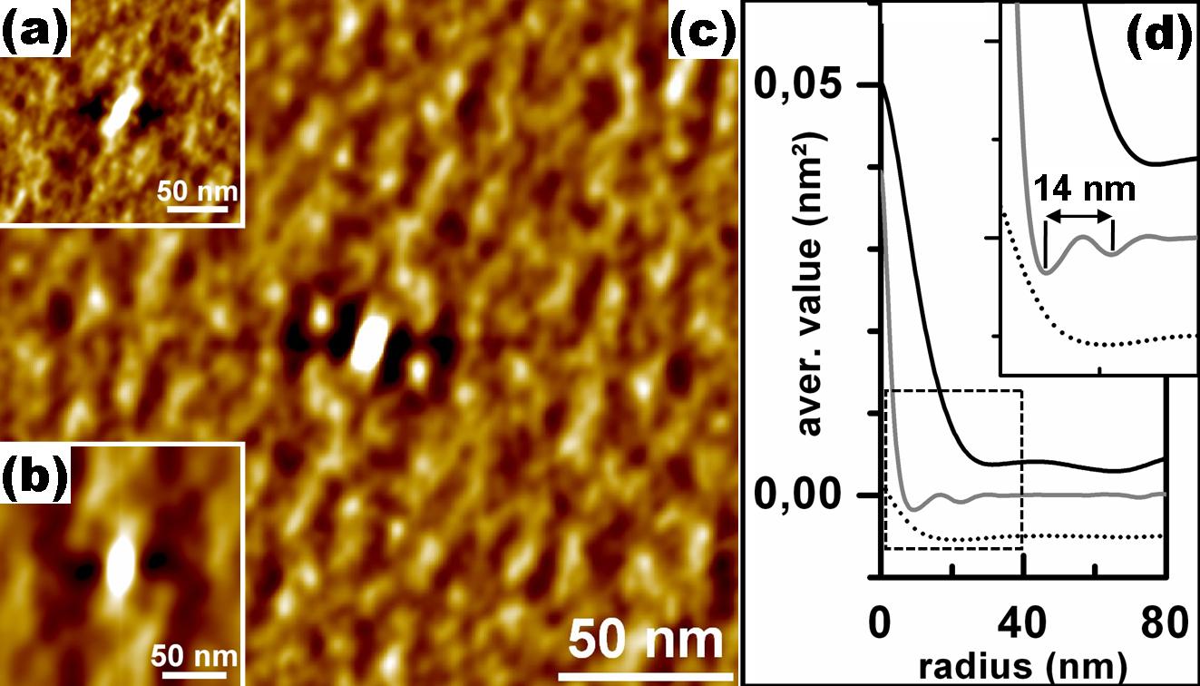
Careful inspection of the graphene monolayer in Fig. 3(a) and (b) shows a modulation on top of the short-range corrugation exhibiting a similar length scale as the corrugation on the SiO2 substrate. In order to disentangle the two contributions, we used two-dimensional autocorrelation functions of the images (a) and (c) Horcas et al. (2007), which are shown in Fig. 4(a) and (b). Note that both figures use the same color scale, i. e. the intensities are directly comparable. A long-range structure represented by a central spot surrounded by four bright areas is visible in both images although with weaker intensity for graphene (a). Fig. 4(c) shows the autocorrelation function of the graphene after removing the long-range part by high-pass filtering using a smooth (first order Butterworth) cutoff at wavelength nm. A preferential short-range distance is clearly visible by the strong spots around the center, but there is additional multiple correlation albeit not with high symmetry. Notice that creep and drift effects are carefully removed from the STM-image using the atomic resolution. We checked the preferential directions visible in both correlation patterns. They are rotating arbitrarily across the SiO2, but we find indication for a preferential orientation on graphene EPAPS . Fig. 4(d) shows radial line sections averaged over all angles of the correlation functions. The SiO2 (black curve) exhibits a correlation length of about 25 nm comparable to Ishigami et al. (2007) and, in addition, a very weak maximum at about 50 nm indicating a slight preferential distance between hills. The gray curve shows the radial line section of the high-pass filtered image of graphene visible in Fig. 4(c). It exhibits a damped oscillation with a wave length of about 14 nm looking very similar to correlation functions of liquids. For comparison, the radial line section of the autocorrelation function of the AFM image after applying the same high-pass filter is shown as a dotted line and does not exhibit any structure. We observe the damped oscillation also after high-pass filtering the original STM image in Fig. 3(a) and determining the autocorrelation function afterwards. In addition, we checked that the obtained wave length is quite robust with respect to slight parameter changes of the filtering process. Depending on the filtering procedure and the selection of the minima or maxima used for determining the wave length, is varying by at maximum nm with a mean value of nm.
From these results, we conclude that monolayer graphene can exhibit a rather regular, liquid-like short-scale corrugation not induced by the substrate. It is similar in height and wavelength to the one observed on suspended graphene Meyer et al. (2007) and calculated for freely suspended graphene by atomic Monte-Carlo methods Fasolino et al. (2007). This observation suggests that the graphene might be partly suspended even on the SiO2. In order to verify this, we compared the Fourier components of the images of graphene and SiO2 within the large wavelengths region nm EPAPS . We indeed find that graphene exhibits an up to 40 % lower amplitude at all wavelengths within this wavelength range. This implies that the graphene does not follow the substrate corrugations exactly, but instead includes areas not in contact with the substrate. We believe that this partly free-standing configuration is the prerequisite for the intrinsic rippling of graphene. Indeed, we have also found other graphene flakes prepared nominally identically by the same person which did not show the intrinsic rippling. This highlights that tiny details of the preparation process can have large impacts on the physical properties, maybe explaining the contradicting weak localization properties in different studies Tikhonenko et al. (2008); Morozov et al. (2006). A comparison of Raman data of several samples indicates that samples with intrinsic rippling are more frequent than samples without EPAPS . Future systematic studies using our method to determine the intrinsic rippling are required.
In summary, we have investigated high-mobility graphene flakes on SiO2 by UHV-STM and scanning tunneling spectroscopy. A mesoscopic corrugation decreasing in amplitude with increasing thickness not induced by the substrate is identified. It is rather regular exhibiting liquid-like correlation properties with a preferential wavelength of about 15 nm and a rms roughness of 0.32 nm. Since the long-range corrugation of the substrate is additionally visible on graphene, but with smaller amplitude than on the substrate, we conclude that the rippled graphene is partly freely suspended.
We gratefully acknowledge useful discussions with G. Güntherodt, U. D. Schwarz and H. Kurz and financial support by FOR 912, project TP 6 of the Deutsche Forschungsgemeinschaft and by the German Federal Ministry of Education and Research (BMBF) under contract number NKNF 03X5508 (”ALEGRA”).
Supplementary information
Histogram of Corrugation
Figure 5 shows representative histograms of the height values on the SiO2 substrate and the graphene sample as obtained by atomic force microscopy (AFM) and scanning tunneling microscopy (STM), respectively. The histograms are based on images of 200 200 nm2 including 512 512 measurement points each. These images are shown in Fig. 3 of the main text. The histogram curves are normalized in order to enclose the same integral area. Gaussian fits are added as guides to the eye. Obviously, the height histogram of Graphene is broader exhibiting a full width at half maximum (FWHM) of 0.78 nm, while SiO2 exhibits a FWHM of only 0.48 nm. While the latter value is quite robust across the surface, the former value is changing by about 25 % across the surface, but is on average larger than the FWHM on SiO2. This demonstrates that the rippling of graphene is not limited to substrate corrugations.
Tip Dependence of Substrate Corrugation
Figure 6 shows two AFM images of the SiO2 substrate obtained in tapping mode by two different tips. Representative scanning electron microscopy (SEM) images of the tips provided by the supplier are added as insets. They are cross-checked by SEM images after the measurements. These images are in agreement with the supplier images, but due to a moderate background pressure, the ultrasharp W-tip fastly burnt away during SEM imaging. The left AFM image is measured by a cantilever with a Si tip having an apex radius of about 10 nm, while the right AFM image is measured with a W tip of nominal tip apex radius of 1 nm mounted at the bottom of the Si tip. Both images exhibit a very similar lateral scale of the corrugation. The rms values are 220 pm and 270 pm, respectively, showing that the tip properties do not significantly change the observed corrugation of the substrate. We cross-checked this result using more than ten images obtained with both tips, which lead to fluctuations in rms values of less than 10%.

Comparison of Correlation Functions
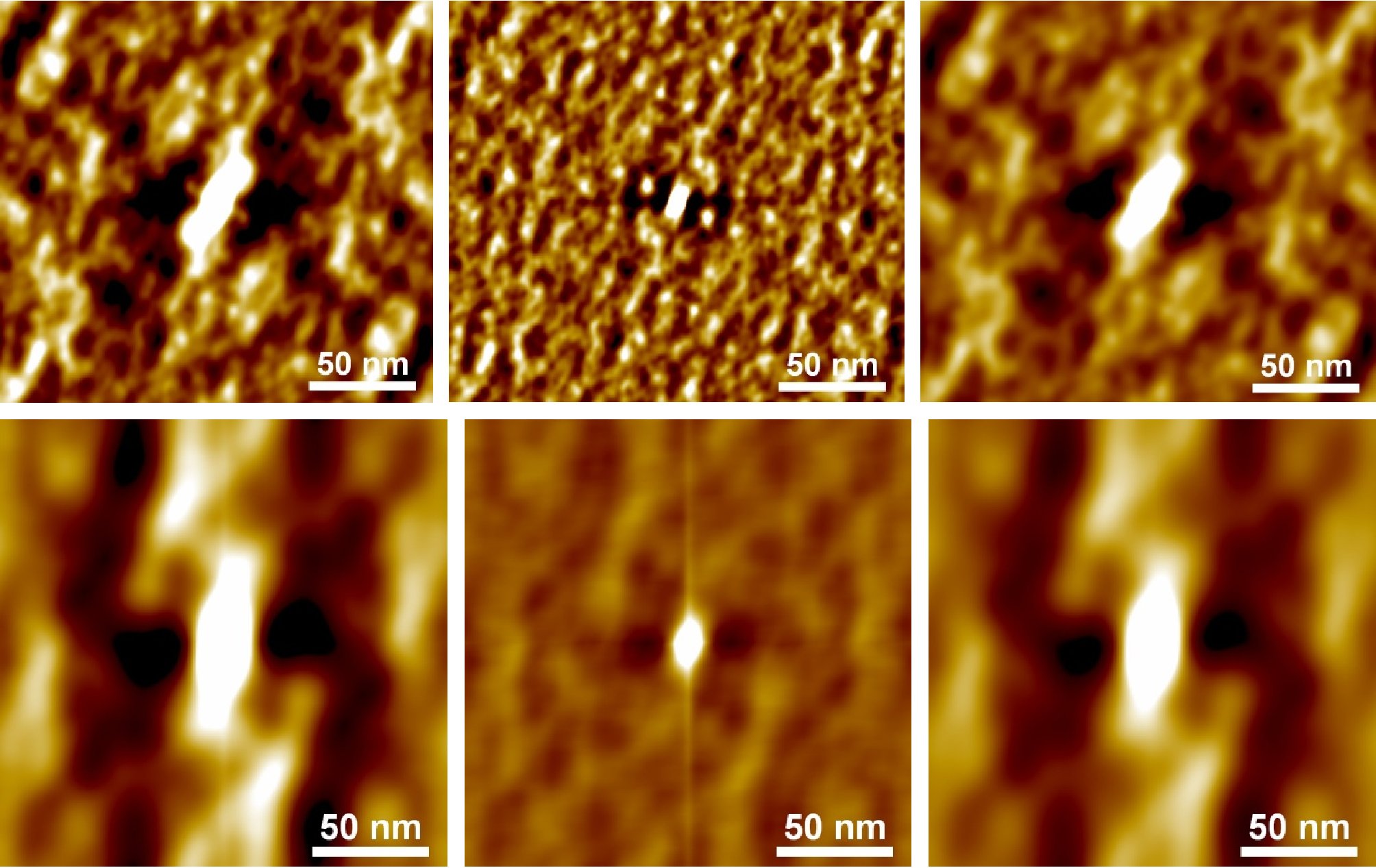
Figure 7 shows a comparison of the correlation functions of the topographic images of graphene (top row) and SiO2 (bottom row). The left column shows the correlation functions directly obtained from the topography. The middle and right column show the high-frequency and low-frequency part of the correlation function separated by a smooth first-order butterworth filter with cutoff wavelength nm. While the large wavelengths visible in the right columns are quite similar in both images, the rather regular short wavelength pattern (middle column) is only observed on graphene. Note that correlation functions within the same columns are scaled to the same contrast, i. e., their brightness is directly comparable.
Reproducibility of Correlation Functions
Figure 8 shows three images (top row) obtained in different areas of the monolayer graphene, separated by several m. They exhibit different rms values of 270 pm, 220 pm and 360 pm (left to right), respectively. The middle row shows the corresponding correlation functions. The bottom row shows the same correlation functions after high-pass filtering using the identical procedure as in Figure 3. Notice that the scales of the images are different. While the long-range corrugation (middle row) is oriented in different directions, the short range corrugations (bottom row) exhibit the same wave length of about 15 nm in all three areas and show a similar orientation as marked by the white lines. The latter indicates that the the short-scale corrugation is related to the atomic directions in graphene. But since the directions of the rippling are fluctuating slightly across the sample similar to the orientations of molecules in liquid crystals, more data are required in order to substantiate the relation between atomic directions and preferred directions of rippling.
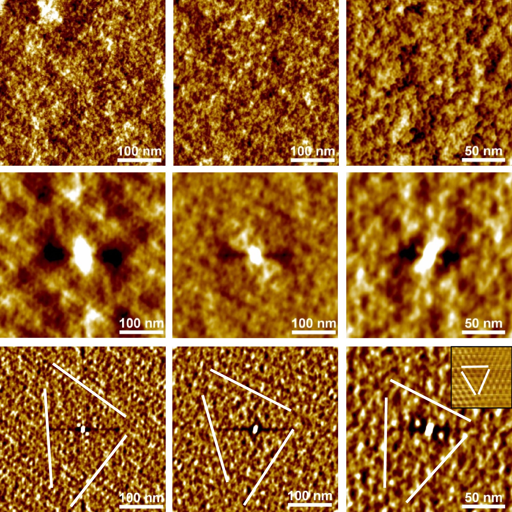
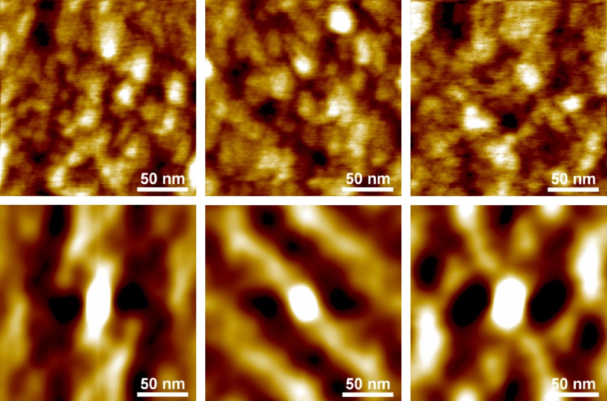
Figure 9 shows topographic images of different areas of the SiO2 substrate (top row) and the corresponding correlation functions (bottom row). They exhibit similar length scales of corrugation but clearly different orientations, which might be due to the polishing procedure of the sample.
Wave Length Dependence of Corrugations
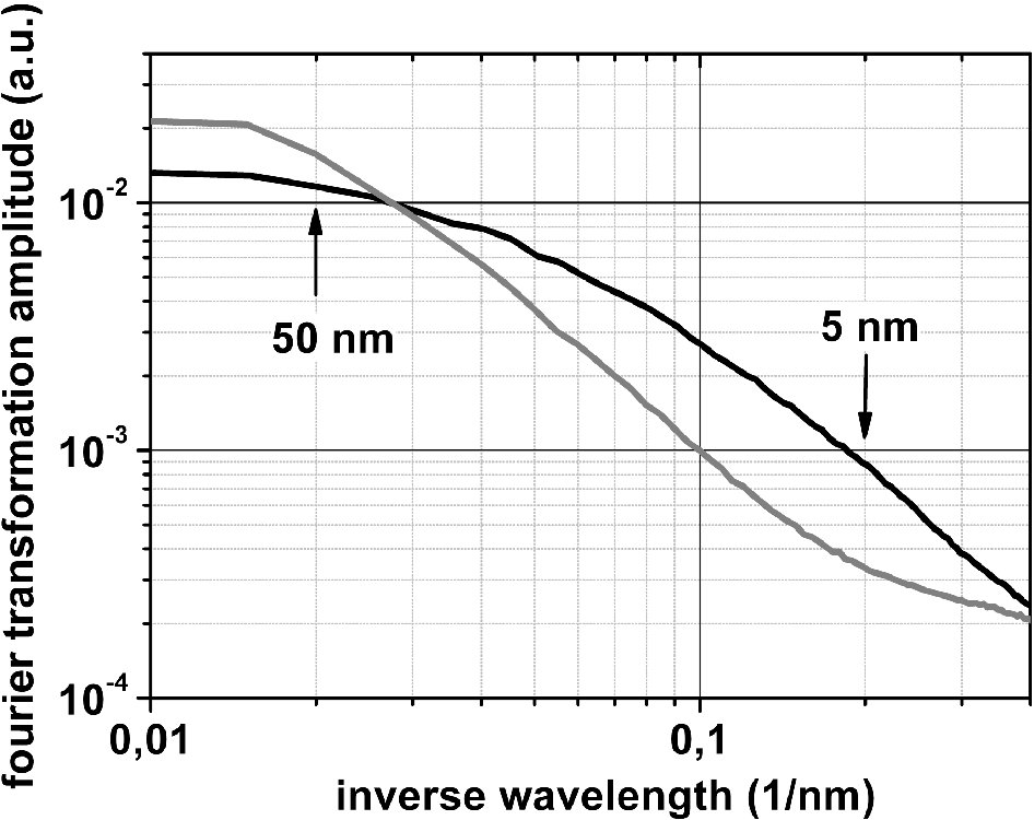
Figure 10 shows the radially averaged Fourrier transforms (FT) of the topographic images of graphene (black curve) and SiO2 (grey curve). The FT curves are based on images of the same lateral size and resolution. The curves are averaged using 10 images of 200 200 nm2 from different areas of the surfaces. Obviously, the corrugation of SiO2 is larger at large wave length (small wave number) down to 30 nm by up to 66 %, while the corrugation on the graphene is larger at smaller wavelengths (larger wave numbers) by up to a factor of 2.6. The individual FTs of different SiO2 areas are nearly indistinguishable, i.e they are not deviating from the width of the grey curve in Fig. 5. However, the FTs of different graphene areas are shifted vertically due to the fluctuating rms value of corrugation, which leads to crossing points of the two curves varying between wavelengths of 20 nm and 40 nm. Importantly, all of the graphene curves show one crossing point with the averaged SiO2 curve.
Raman investigations on monolayer graphene
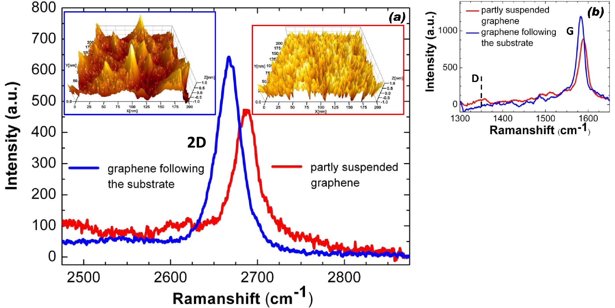
In order to observe the influence of the graphene film morphology on Raman scattering, we compared Raman spectra (laser wave length 532.1 nm), taken in identical experimental conditions, of a monolayer flake which is partly suspended and one that follows the substrate (Fig. 11). The surface structure of these samples was determined using STM measurements (Insets Fig. 11a). The Raman spectra were recorded before and after the STM measurements giving the same result. A difference between both spectra regarding the positions of the 2D and G peaks is clearly visible. The wave number of the 2D peak is 2686.7 cm-1 for the partly suspended graphene flake and 2670.5 cm-1 for the flake following the substrate. Hence, it results that the change in morphology causes a shift of the 2D peak by 16.2 cm-1 (Fig. 11a). A similar effect was observed at the G peak which is shifted by 5.5 cm-1 to lower values for the flake following the substrate (Fig. 11b). The D peak (about 1350 cm-1) is barely visible for both samples indicating a good quality of our graphene. Raman spectra of several of our graphene samples (about 15) prepared in nominally identical conditions show more frequently a non shifted 2D line with an average value of 2692.45.3 cm-1. Hence, we conclude that our samples mostly exhibit intrinsic rippling. If we compare with wave numbers of the 2D line within the literature using only the data taken with a similar laser wave length (514 - 532 nm) Ferrari et al. (2006); Gupta et al. (2006); Graf et al. (2007), we find 2680 - 2700 cm-1. Hence, we believe that the majority of samples investigated so far exhibit intrinsic rippling as displayed in the right inset of Figure 7a.
References
- Mermin (1968) N. D. Mermin, Phys. Rev. 176, 250 (1968).
- Novoselov et al. (2004) K. S. Novoselov, A. K. Geim, S. V. Morozov, D. Jiang, Y. Zhang, S. V. Dubonos, I. V. Grigorieva, and A. A. Firsov, Science 306, 666 (2004).
- Zhang et al. (2005) Y. Zhang, J. W. Tan, H. L. Stormer, and P. Kim, Nature 438, 201 (2005).
- Geim and Novoselov (2007) A. K. Geim and K. S. Novoselov, Nature Mat. 6, 183 (2007).
- Katsnelson et al. (2006) M. I. Katsnelson, K. S. Novoselov, and A. K. Geim, Nature Phys. 2, 620 (2006).
- Novoselov et al. (2007) K. S. Novoselov, Z. Jiang, Y. Zhang, S. V. Morozov, H. L. Stormer, U. Zeitler, J. C. Maan, G. S. Boebinger, P. Kim, and A. K. Geim, Science 315, 1379 (2007).
- Tombros et al. (2007) N. Tombros, C. Jozsa, M. Popinciuc, H. T. Jonkman, and B. J. van Wees, Nature 448, 571 (2007).
- Son et al. (2006) Y. W. Son, M. L. Cohen, and S. G. Louie, Nature 444, 347 (2006).
- Morozov et al. (2006) S. V. Morozov, K. S. Novoselov, M. I. Katsnelson, F. Schedin, L. A. Ponomarenko, D. Jiang, and A. K. Geim, Phys. Rev. Lett. 97, 016801 (2006).
- McCann et al. (2006) E. McCann, K. Kechedzhi, V. I. Fal’ko, H. Suzuura, T. Ando, and B. L. Altshuler, Phys. Rev. Lett. 97, 146805 (2006).
- Meyer et al. (2007) J. C. Meyer, A. K. Geim, M. I. Katsnelson, K. S. Novoselov, T. J. Booth, and S. Roth, Nature 446, 60 (2007).
- Fasolino et al. (2007) A. Fasolino, J. H. Los, and M. I. Katsnelson, Nature Mat. 6, 858 (2007).
- Morozov et al. (2008) S. V. Morozov, K. S. Novoselov, M. I. Katsnelson, F. Schedin, D. Elias, J. A. Jaszczak, and A. K. Geim, Phys. Rev. Lett. 100, 016602 (2008).
- Stolyarova et al. (2007) E. Stolyarova, K. T. Rim, S. Ryu, J. Maultzsch, P. Kim, L. E. Brus, T. F. Heinz, M. S. Hybertsen, and G. W. Flynn, Proc. Natl. Acad. Sci. 104, 9209 (2007).
- Ishigami et al. (2007) M. Ishigami, J. H. Chen, W. G. Cullen, M. S. Fuhrer, and E. D. Williams, Nano Lett. 7, 1643 (2007).
- Tikhonenko et al. (2008) F. V. Tikhonenko, D. W. Horsell, R. V. Gorbachev, and A. K. Savchenko, Phys. Rev. Lett. 100, 056802 (2008).
- Zhang et al. (2008) Y. Zhang, V. W. Brar, F. Wang, C. Girit, Y. Yayon, M. Panlasigui, A. Zettl, and M. F. Crommie, arXiv:0802.4315v1 (2008).
- Lemme et al. (2007) M. C. Lemme, T. J. Echtermeyer, M. Baus, and H. Kurz, IEEE Elect. Dev. Lett. 28, 282 (2007).
- Ferrari et al. (2006) A. C. Ferrari, J. C. Meyer, V. Scardaci, C. Casiraghi, M. Lazzeri, F. Mauri, S. Piscanec, D. Jiang, K. S. Novoselov, S. Roth, et al., Phys. Rev. Lett. 97, 187401 (2006).
- Lemme et al. (2008) M. Lemme, T. Echtermeyer, M. Baus, B. Szafranek, J. Bolten, M. Schmidt, T. Wahlbrink, and H. Kurz, Solid-State Electronics 52, 514 (2008).
- Tan et al. (2007) Y. W. Tan, Y. Zhang, K. Bolotin, Y. Zhao, S. Adam, E. H. Hwang, S. Das Sarma, H. L. Stormer, and P. Kim, Phys. Rev. Lett. 99, 246803 (2007).
- Wiebe et al. (2004) J. Wiebe, A. Wachowiak, F. Meier, D. Haude, T. Foster, M. Morgenstern, and R. Wiesendanger, Rev. Sci. Instrum. 75, 4871 (2004).
- (23) V. Geringer, S. Runte, M. Liebmann, and M. Morgenstern, to be published.
- (24) MikroMasch (www.spmtips.com), NSC15 (Si) and DP15/HiRes-W/AlBS (Si cantilever with W tip apex).
- Hölscher and Schwarz (2007) H. Hölscher and U. D. Schwarz, Int. J. Non-Linear Mech. 42, 608 (2007).
- Wittneven et al. (1998) C. Wittneven, R. Dombrowski, M. Morgenstern, and R. Wiesendanger, Phys. Rev. Lett. 81, 5616 (1998).
- Stroscio et al. (1986) J. A. Stroscio, R. M. Feenstra, and A. P. Fein, Phys. Rev. Lett. 57, 2579 (1986).
- Brar et al. (2007) V. W. Brar, Y. Zhang, Y. Yayon, T. Ohta, J. L. McChesney, A. Bostwick, E. Rotenberg, K. Horn, and M. F. Crommie, Appl. Phys. Lett. 91, 122102 (2007).
- Rutter et al. (2007) G. M. Rutter, J. N. Crain, N. P. Guisinger, T. Li, P. N. First, and J. A. Stroscio, Science 317, 219 (2007).
- Lauffer et al. (2008) P. Lauffer, K. V. Emtsev, R. Graupner, T. Seyller, L. Ley, S. A. Reshanov, and H. B. Weber, Phys. Rev. B 77, 155426 (2008).
- Horcas et al. (2007) I. Horcas, R. Fernández, J. M. Gómez-Rodríguez, J. Colchero, J. Gómez-Herrero, and A. M. Baro, Rev. Sci. Instrum. 78, 013705 (2007).
- (32) See supplementary information.
- Gupta et al. (2006) A. Gupta, G. Chen, P. Joshi, S. Tadigadapa, and P. Eklund, Nano Letters 6, 2667 (2006).
- Graf et al. (2007) D. Graf, F. Molitor, K. Ensslin, C. Stampfer, A. Jungen, C. Hierold, and L. Wirtz, Nano Letters 7, 238 (2007).