Adv. in At. Mol. Opt. Physics 48, 263-356 (2002)
Microscopic atom optics: from wires to an atom chip
Abstract
We give a comprehensive overview of the development of micro traps, from the first experiments on guiding atoms using current carrying wires in the early 1990’s to the creation of a BEC on an atom chip.
I Introduction
Scientific and technological progress in the last decades has proven that miniaturization and integration are an important step towards the robust application of fundamental physics. Be it electronics and semiconductor physics in integrated circuits, or optics in micro optical devices and sensors. The experimental effort described in this work aims at the goal to achieve the same for matter wave optics.
Matter wave optics beautifully illustrates quantum behavior. Realizations using neutral atoms are attractive because of the well established techniques to coherently manipulate internal and external degrees of freedom, and their weak coupling to the environment. Miniaturizing electric and magnetic potentials is essential to building very versatile traps and guides for atoms at a scale (m) which will enable controlled quantum manipulation and entanglement. Integration with other quantum optics, micro optics and photonics techniques will allow for the robust creation, manipulation and measurement of atomic quantum states in these micro traps. In our vision we see a monolithic integrated matter wave device which will allow us to establish a new experimental toolbox and enable new insights into fundamental quantum physics for example in issues such as decoherence, entanglement and non linearity, low-dimensional mesoscopic systems, and degenerate quantum gases (Bosons and Fermions) beyond mean field. A successful implementation may lead to wide spread applications from highly sensitive sensors (time and acceleration) to quantum information technology.
The goal of this review is to sum up our year long exciting journey into the miniaturization and integration of matter wave optics resulting in devices mounted on surfaces, so called atom chips. It brought together the best of two worlds, the vast knowledge of quantum optics and matter wave optics and the mature techniques of micro fabrication.
The first experiments started in the early 1990s with the guiding of atoms with free standing wires and investigating the trapping potentials in simple geometries. This lead later to the micro fabrication of atom optical elements down to m size on atom chips. Very recently the simple creation of a Bose-Einstein condensation in miniaturized surface traps was achieved, and the first attempts to integrate light optics on the atom chip are in progress. Even though there are many open questions, we firmly believe that we are only at the beginning of a new era of robust quantum manipulation of atomic systems, with many applications.
The review is organized as follows. We begin in section II by describing microscopic atom optical elements using current carrying and charged structures, acting as sources for electric and magnetic fields which interact with the atom. In the following sections we describe first the experiments with free standing structures - the so called atom wire (section III), investigating the basic principles of microscopic atom optics, and then the miniaturization on the atom chip (section IV). In section V we discuss one of the central open questions: what happens with cold atoms close to a warm surface, how fast will they heat up, and how fast will they lose their coherence? The role of technical noise, the fundamental noise limits and the influence of atom–atom and atom–surface interactions, are discussed. We then conclude with an outlook of what we believe the future directions to be, and what can be hoped for (section VI).
The scientific progress regarding manipulation of atoms close to surfaces was enormous within the last decade. Besides the atom-wire and atom chip described here, it ranges a whole spectrum: from reflection experiments on atom mirrors, to studying Van der Waals interactions and quantum reflection; from the use of micro magnets to trap atoms, to evanescent light field traps. Many of these have been reviewed recently, and will not be included here. We will almost exclusively concentrate on manipulation of atoms with static microscopic electric and magnetic fields created by charged and/or current carrying (microscopic) structures. For related experiments and proposals, which are not discussed in this review, we refer the reader to the excellent reviews referenced throughout the text e.g. (Dowling and Gea-Banacloche, 1996; Grimm et al., 2000; Hinds and Hughes, 1999).
II Designing microscopic atom optics
Neutral atoms can be manipulated by means of their interaction with magnetic, electric, and optical fields. In this review the emphasis is put on the magnetic and the electric interaction. The designing of traps and guides using charged and current carrying structures and the combination of different types of interaction to form devices for guided matter wave optics are discussed. It is shown how miniaturization of the structures leads to great versatility where a variety of potentials can be tailored at will. We start with some general statements and focus then on the concepts that are important for surface mounted structures and address issues of miniaturization and its technological implications.
II.1 Magnetic interaction
A particle with total spin and magnetic moment experiences the potential
| (1) |
where is the Bohr magneton, the Landé-factor of the atomic hyperfine state, and the magnetic quantum number. In general, the vector coupling results in a complicated motion of the atom. However, if the Larmor precession () of the magnetic moment is much faster than the apparent change of direction of the magnetic field in the rest frame of the moving atom, an adiabatic approximation can be applied. The magnetic moment then follows the direction of the field adiabatically, is a constant of motion, and the atom is moving in a potential proportional to the modulus of the magnetic field .
Depending on the orientation of relative to the direction of a static magnetic field, we distinguish two cases:
(1) If the magnetic moment is pointing in the same direction as the magnetic field (), an atom is drawn towards increasing fields, therefore it is in a strong field seeking state. This state is the lowest energy state of the system. Minima of the potential energy are found at maxima of the field. Maxima of the magnetic field in free space are, however, forbidden by the Earnshaw theorem111The Earnshaw theorem can be generalized to any combination of electric, magnetic and gravitational field (Wing, 1984; Ketterle and Pritchard, 1992).. This means that for trapping atoms in the strong field seeking state, a source of the magnetic field, such as a current carrying material object or an electron beam, has to be located inside the trapping region.
(2) If the magnetic moment of an atom is pointing in the direction opposite to the magnetic field (), the atom is repelled from regions with high magnetic fields; it is then in the metastable weak field seeking state. In this case, minima of the modulus of the field correspond to potential minima. Because a minimum of the modulus of the magnetic field in free space is not forbidden by the Earnshaw theorem, traps of this type are most common for neutral atom trapping. Losses from the traps are a potential problem (see section V), especially when non adiabatic transitions to the energetically lower high field seeking states become likely in regions of low or even vanishing fields.
II.1.1 Kepler guide
A possible realization of a trap for an atom in the strong field seeking state is a current carrying wire with the atom orbiting around it (Vladimirskii, 1961; Schmiedmayer, 1992, 1995a, 1995b; Schmiedmayer and Scrinzi, 1996a, b; Denschlag, 1998; Denschlag et al., 1999a). The interaction potential is given by:222This and all other expressions for magnetic and electric fields in this section are given in the limit of an infinitely thin wire, unless stated otherwise.
| (2) |
where is the current through the wire, is the azimuthal unit vector in cylindrical coordinates, and mmG/A is the vacuum permeability. This potential has the form of a Coulomb potential, but the coupling is vectorial. Using the adiabatic approximation, corresponds to a 2-dimensional scalar () potential, in which atoms move in Kepler orbits.333From corrections to the adiabatic approximation to the next order, we obtain an effective Hamiltonian for the orbital motion of the atom where the Coulomb-like binding potential is corrected by a small repulsive interaction (Shapere and Wilczek, 1989; Aharonov and Stern, 1992; Stern, 1992; Littlejohn and Weigert, 1993; Schmiedmayer and Scrinzi, 1996a, b). As a result, the adiabatic orbits are Kepler-like, and show an additional precession around the wire. A very similar potential can be realized for small polar molecules with a permanent dipole moment interacting with the electric field of a charged wire (Sekatskii and Schmiedmayer, 1996).
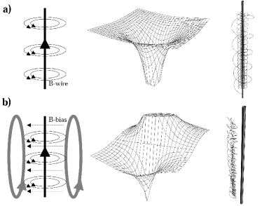
In the quantum regime, the system looks like a 2-dimensional hydrogen atom in a (nearly circular) Rydberg state. The wire resembles the “nucleus” and the atom takes the place of the “electron”. Considerable theoretical work has been published on the quantum mechanical treatment of this system showing a hydrogen-like energy spectrum (Pron’kov and Stroganov, 1977; Blümel and Dietrich, 1989, 1991; Voronin, 1991; Hau et al., 1995; Burke et al., 1996; Berg-Sørensen et al., 1996; Schmiedmayer and Scrinzi, 1996a, b).
The magnetic field, the potential, and typical classical trajectories are presented in Fig. 1a.
II.1.2 Side guide
Originally, Frisch and Segrè (1933) presented the idea that a current carrying wire () and a homogeneous bias field () may produce a well defined 2-dimensional field minimum, in the form of a quadrupole field (Fig. 1b). The bias field cancels the circular magnetic field of the wire along a line parallel to the wire at a distance
| (3) |
Around this line the modulus of the magnetic field increases in all directions and forms a tube with a magnetic field minimum at its center. Atoms in the weak field seeking state can be trapped in this 2-dimensional quadrupole field and be guided along the side of the wire, i.e. in a side guide. At the center of the trap the magnetic field gradient is
| (4) |
If the bias field is orthogonal to the wire, the two fields cancel exactly, and trapped atoms can be lost due to Majorana transitions between trapped and untrapped spin states (see section V.1). This problem can be circumvented by adding a small B-field component along the wire direction which lifts the energetic degeneracy between the trapped and untrapped states. This potential is conventionally called a Ioffe-Pritchard trap (Gott et al., 1962; Pritchard, 1983; Bagnato et al., 1987). At the same time, the potential form of the guide near the minimum changes from linear to harmonic. The guide is then characterized by the curvature in the transverse directions
| (5) |
In the harmonic oscillator approximation, the trap frequency is given by
| (6) |
where is the mass of the atom.

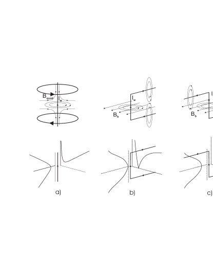
When mounting the wire onto a surface, the bias field has to have a component parallel to the surface in order to achieve a side guide above the surface. The bias field can be formed by two additional wires on each side of the guiding wire. The direction of the current flow in these wires has to be opposite to the current in the guiding wire (Fig. 2). This is especially interesting because the wires can be mounted on the same chip, and a self sufficient guide can be obtained.
II.1.3 Two wire guides
Counter-propagating currents
A different way to create a guide is by using two parallel wires with counter-propagating currents with a bias field which has a component orthogonal to the plane containing the two wires (Fig. 2)(Thywissen et al., 1999a).
The important advantage of this configuration is that the two wires and therefore the atom guide can be bent in an arbitrary way in the plane perpendicular to the bias field, whereas in the single wire guide the direction is restricted to angles close to the line perpendicular to the bias field. If there is an additional bias field applied along the wires, a Ioffe-Pritchard guide is obtained. Again, two added wires can replace the external bias fields (see section IV for an example of an experimental implementation).

The field generated by the wires compensates the bias field at a distance:
| (7) |
where is the distance between the two wires. When the field from the wires is not capable of compensating the bias field. Two side guides are then obtained, one along each wire in the plane of the wires.
In the case , the gradient in the confining directions is given by
| (8) |
If there is a field component along the wire, the position of the guide is unchanged. However, the shape of the potential near its minimum is harmonic, the curvature in the radial direction is given by:
| (9) |
In the special case of , the gradient and, for the case of a non vanishing , the curvature of the potential at the minimum position, are exactly equal to the corresponding magnitudes for the single wire guide.
Co-propagating currents
The magnetic fields formed by two parallel wires carrying co-propagating currents vanishes along the central line between the wires and increases and changes direction like a 2-dimensional quadrupole. The wires form a guide as shown in Fig. 3 allowing atoms to be guided around curves (Müller et al., 1999). It is even possible to hold atoms in a storage ring formed by two closed wire (Sauer et al., 2001) (section III.1.7). When aiming at miniaturized, surface mounted structures, the fact that the potential minimum is located between the wires rather than above them, has to be considered.

When a bias field parallel to the plane of the wires is added, the potential minimum moves away from the wire plane and a second quadrupole minimum is formed at a distance far above the wire plane where the two wires appear as a single wire carrying twice the current (see side guide in section II.1.2). Depending on the distance between the wires with respect to the characteristic distance
| (10) |
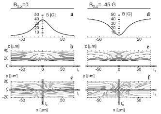
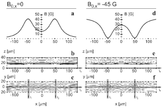
one observes three different cases (Fig. 4): (i) If , two minima are created one above the other on the axis between the wires. In the limit of going to zero, the barrier potential between the two minima goes to infinity and the minimum closer to the wire plane falls onto it; (ii) if , the two minima fuse into one, forming a harmonic guide; (iii) if two minima are created one above each wire. Splitting and recombination can be achieved by simply increasing and lowering the bias field (Denschlag, 1998; Zokay and Garraway, 2000; Hinds et al., 2001).
Finally we mention a proposal by Richmond et al. (1998) where a tube consisting of two identical, interwound solenoids carrying equal but opposite currents can be used as a low field seeker guide. The magnetic field is almost zero throughout the center of the tube, but it increases exponentially as one approaches the walls formed by the current carrying wires. Hence, cold low-field-seeking atoms passing through the tube should be reflected by the high magnetic fields near the walls, which form a magnetic mirror.
Examples of typical guiding parameters for the alkali atoms lithium and rubidium trapped in single and two wire guides are given in table 1. Trap frequencies in the order of 1 MHz or above can be achieved with moderate currents and bias fields. The guided atoms are then located a few m above the surface.
II.1.4 Simple traps
An easy way to build traps is to start from the guides discussed above, and close the trapping potential by ‘endcaps’. This can be accomplished by taking advantage of the fact that the magnetic field is a vector field, and the interaction potential is scalar (eq. 1). By changing the angle between the wire and the bias field, one can change the minimum of the potential and close the trap. Simple geometries are either a straight guide and an inhomogeneous bias field, or a homogeneous bias field in combination with a bent wire.
| side guide | ||||||||
| wire | bias fields | potential | ground state | |||||
| current | depth | dist. | grad. | energy | size | life time | ||
| mA | [G] | [G] | [mK] | [m] | [kG/cm] | [kHz] | [nm] | [ms] |
| Li | ||||||||
| 1000 | 80 | 2 | 5.4 | 25 | 32 | 100 | 120 | |
| 500 | 200 | 10 | 13 | 5 | 400 | 570 | 50 | |
| 200 | 400 | 30 | 27 | 1 | 4000 | 3300 | 21 | 7 |
| Rb | ||||||||
| 1000 | 80 | 1 | 5.4 | 25 | 32 | 41 | 53 | |
| 500 | 200 | 4 | 13 | 5 | 400 | 250 | 21 | |
| 200 | 400 | 20 | 27 | 1 | 4000 | 1100 | 10 | |
| 1000 | 2000 | 50 | 130 | 1 | 20000 | 3600 | 6 | |
| two wire guide (counter-propagating currents) | ||||||||
| Li | ||||||||
| 1000 | 80 | 2 | 5.4 | 25 | 32 | 100 | 120 | |
| 500 | 200 | 10 | 13 | 5 | 400 | 570 | 50 | |
| 100 | 130 | 10 | 8.7 | 1.5 | 870 | 1200 | 34 | 5 |
| Rb | ||||||||
| 1000 | 80 | 1 | 5.4 | 25 | 32 | 41 | 53 | |
| 500 | 200 | 4 | 13 | 5 | 400 | 250 | 21 | |
| 100 | 130 | 5 | 8.7 | 1.5 | 870 | 490 | 15 | 185 |
Straight guide and an inhomogeneous bias field
Examples for traps formed by superposing an inhomogeneous bias field and the field of a straight wire use quadrupole fields because the complete change of direction in addition to the inhomogenity is needed to close the trap. An interesting fact is that a current carrying wire on the symmetry axis of a quadrupole field can be used to ‘plug’ the zero of the field. In this configuration a ring shaped trap is formed (Fig. 5a) that has been demonstrated experimentally (Denschlag, 1998; Denschlag et al., 1999b). In the Munich (now Tübingen) group of C. Zimmermann a modified version of this type of trap with the wire displaced from the quadrupole axis (Fortagh et al., 1998, 2000) was used to create a Bose-Einstein condensate on an atom chip (Ott et al., 2001).
Bent wire traps: the U- and Z-trap
3-dimensional magnetic traps can be created by bending the current carrying wire of the side guide (Cassettari et al., 1999; Reichel et al., 1999; Haase et al., 2001). The magnetic field from the bent leads creates endcaps for the wire guide, confining the atoms along the central part of the wire. The size of the trap along this axis is then given by the distance between the endcaps. Here we describe two different geometries:
(1) Bending the wire into a “U”-shape (Fig. 5b) creates a magnetic field that in combination with a homogeneous bias field forms a 3-dimensional quadrupole trap444The minimum of the U-trap is displaced from the central point of the bar, in a direction opposite to the bent wire leads. A more symmetric quadrupole can be created by using 3 wires in an H configuration. There the side guide is closed by the two parallel wires crossing the central wire orthogonally. The trap is then in between the two wires, along the side guide wire.. The geometry of the bent leads results in a field configuration where a rotation of the bias field displaces the trap minimum but the field always vanishes completely at this position.
(2) A magnetic field zero can be avoided by bending the wire ends to form a “Z” (Fig. 5c). Here, one can find directions of the external bias field where there are no zeros in the trapping potential, for example when the bias field is parallel to the leads. This configuration creates a Ioffe-Pritchard type trap.
The potentials for the U- and the Z-trap scale similarly as for the side guide, but the finite length of the central bar and the directions of the leads have to be accounted for. Simple scaling laws only hold as long as the distance of the trap from the central wire is small compared to the length of the central bar (Cassettari et al., 1999; Reichel et al., 1999; Haase et al., 2001). Finally, one should note that bending both Z leads once more, resulting in 3 parallel wires, again supplies the needed bias field, creating a self sufficient Z-trap.
Crossed wires
Another way to achieve confinement in the direction parallel to the wire in a side guide is to run a current through a second wire that crosses the original wire at a right angle. creates a magnetic field with a longitudinal component which is maximal at the position of the side guide that is closest to the additional wire. Adding a longitudinal component to the bias field, i.e. rotating , results in an attractive potential confining the atoms in all three dimensions. As a side effect position and shape of the potential minimum are altered by the vertical component of . Fig. 6 illustrates this type of trap configuration. Experiments of the Munich group have proven this concept to be feasible (see section IV.3.1 and Fig. 34) and it was suggested to use the two wire cross as a basic module for implementing complex trapping and guiding geometries (Reichel et al., 2001).
II.1.5 Weinstein-Libbrecht traps
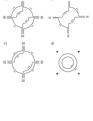
Even more elaborate designs for traps than the ones described previously can be envisioned. As an example we refer the reader to ideas of Weinstein and Libbrecht (1995). They describe planar current geometries for constructing microscopic magnetic traps (multipole traps, Ioffe traps and dynamical traps). We focus here on the Ioffe trap proposals. Fig. 7 shows four possible geometries: (a) three concentric half loops; (b) two half loops with an external bias field; (c) one half loop, one full loop and a bias field; (d) two full loops with a bias field and external Ioffe bars. The first of these, which we refer to as Ioffe (a), is essentially a planar analog of the nonplanar Ioffe trap with two loops and four Ioffe bars. The Ioffe (b) configuration replaces one of the loops with a bias field. The Ioffe (c) configuration is similar to Ioffe (b) but provides a steeper trapping potential on axis and weaker trapping in the perpendicular directions; this makes an overall deeper trap with greater energy-level splitting for given current and size. The Ioffe (d) is a hybrid configuration, which uses external (macroscopic) Ioffe bars to produce the 2-dimensional quadrupole field, while deriving the on-axis trapping fields from two loops and a bias field. This is a reasonable configuration since macroscopic coils can generate quadrupole fields that are nearly as large as those from microscopic coils. Typical energy splittings in the range of 1MHz are achievable using experimentally realistic parameters (Drndić et al., 1998).
II.1.6 Arrays of traps
The various tools for guiding and trapping discussed above can be combined to form arrays of magnetic microtraps on atom chips. Especially suitable for this purpose is the technique of the crossed wires which requires, however, a multilayer fabrication of the wires on the surface. Arrays of traps and their applications, especially in quantum information processing, are discussed in the outlook section VI.
II.1.7 Moving potentials
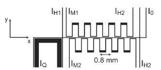
Introducing time dependent potentials facilitates arbitrary movement of atoms from one location to another. There are different proposals for possible implementations of such ‘motors’ or ‘conveyor belts’, one of which has already been demonstrated experimentally by Hänsel et al. (2001a): Using solely magnetic fields it is based on an approximation of the crossed wire configuration. Atoms trapped in a side guide potential are confined in the longitudinal direction by two auxiliary meandering wires (Fig. 8). By running an alternating current through both auxiliary wires with a relative phase difference of , the potential minimum moves along the guide from one side to the other in a controllable way. In section IV we present experimental results of the above scheme.
II.1.8 Beam splitters
By combining two of the above described guides, it is possible to design potentials where at some point two different paths are available for the atom. This can be realized using different configurations (examples are shown in Fig. 9) some of which have already been demonstrated experimentally (see section IV).
Y-beam splitters
A side guide potential can be split by forking an incoming wire into two outgoing wires in a Y-shape (Fig. 9a). Similar potentials have been used in photon and electron interferometers555The Y-configuration has been studied in quantum electronics by Palm and Thylén (1992, 1999). (Buks et al., 1998). A Y-shaped beam splitter has one input guide for the atoms, that is the central wire of the Y, and two output guides corresponding to the right and left wires. Depending on how the current in the input wire is sent through the Y, atoms can be directed to the output arms of the Y with any desired ratio. This simple configuration has been investigated by Cassettari et al. (2000) (see sections III.1.3 and IV.3.3 for experimental realizations). Its disadvantages are: 1) In a single wire Y-beam splitter the two outgoing guides are tighter and closer to the surface than the incoming guide. The changed trap frequency and the angle between incoming and outgoing wires lead to a change of field strength at the guide minimum and can cause backscattering from the splitting point. 2) In the Ioffe-Pritchard configuration (i.e. with an added longitudinal bias field), the splitting is not fully symmetric due to different angles of the outgoing guides relative to the bias field. 3) A fourth guide leads from the splitting point to the wire plane, i.e. the surface of the chip.
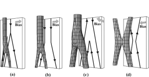
The backscattering and the inaccessible fourth guide of the Y-beam splitter may be, at least partially, overcome using different beam splitter designs like the ones shown in Fig. 9b,c. The configuration shown in Fig. 9b has two wires which run parallel up to a given point and then separate. If the bias field is chosen so that the height of the incoming guide is equal to the half distance of the wires ( as defined in eq. 10 in section II.1.3), the height of the potential minimum above the chip surface is maintained throughout the device (in the limit of a small opening angle) and no fourth port appears in the splitting region. The remaining problem of the possible reflections from the potential in the splitting region can be overcome by the design presented in Fig. 9c. Here, a wave guide is realized with two parallel wires with currents in opposite directions and a bias field perpendicular to the plane of the wires. This type of design creates a truly symmetric beam splitter where input and output guides have fully identical characteristics.
X-beam splitters
A different possible beam splitter geometry relies on the tunneling effect: Two separate wires are arranged to form an X, where both wires are bent at the position of the crossing in such a way that they do not touch (see Fig. 9d). An added horizontal bias field forms two side guides that are separated by a barrier that can be adjusted to be low enough to raise the tunneling probability considerably at the point of closest approach. If the half distance between the wires becomes as small as , the barrier vanishes completely, resulting in a configuration that is equivalent to the combination of two Y-beam splitters (Müller et al., 2000). The choice of the parameters in the wire geometry, the wire current, and the bias field govern the tunneling probability and thereby the splitting ratio in this type of beam splitter. The relative phase shift between the two split partial waves in a tunneling beam splitter allows to combine two beam splitters to form a Mach-Zehnder interferometer. Another advantage of the X-beam splitter is that the potential shape in the inputs and outputs stays virtually the same all over the splitting region as opposed to the Y-beam splitter. A detailed analysis of the tunneling X-beam splitter can be found in Andersson et al. (1999).
For an ideal symmetric Y-beam splitter, coherent splitting for all transverse modes should be achieved due to the definite parity of the system (Cassettari et al., 2000). This was confirmed with numerical 2-dimensional wave packet propagation for the lowest 35 modes. The 50/50 splitting independent of the transverse mode is an important advantage over four way beam splitter designs relying on tunneling such as the X-beam splitter described above. For the X-beam splitter, the splitting ratios for incoming wave packets are very different for different transverse modes, since the tunneling probability depends strongly on the energy of the particle. Even for a single mode, the splitting amplitudes, determined by the barrier width and height, are extremely sensitive to experimental noise.
II.1.9 Interferometers
Following the above ideas of position dependent multiple potentials and time dependent potentials which are able to split minima in two and recombine them, several proposals for chip based atom interferometers have been put forward (Hinds et al., 2001; Hänsel et al., 2001b; Andersson et al., 2002).
Interferometers in the spatial domain
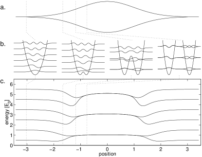
To build an interferometer for guided atoms (Andersson et al., 2002) two Y-beam splitters can be joined back to back (Fig. 10a). The first acts as splitter and the second as recombiner. The eigenenergies of the lowest transverse modes along such an interferometer in 2-dimensional geometry666In 2-dimensional confinement the out of plane transverse dimension is either subject to a much stronger confinement or can be separated out. For experimental realization see (Gauck et al., 1998; Spreeuw et al., 2000; Hinds et al., 2001; Pfau, 2001) are depicted in Fig. 10c. From the transverse mode structure one can see that there are many disjunct interferometers in Fock space. Each of them has two transverse input modes ( and , being the energy quantum number of the harmonic oscillator) and two output modes. In between the two Y-beam splitters, the waves propagate in a superposition of and in the left and right arm, respectively. With adiabaticity fulfilled, the disjunct interferometers are identical.
Considering any one of these interferometers, an incoming transverse state evolves after the interferometer into a superposition of the same and the neighboring transverse outgoing state (Fig. 10c), depending on the phase difference acquired between and during the spatial separation of the wave function777The relative phase shift between the two spatial arms of the interferometer can be introduced by a path length difference or by adjusting the potentials to be slightly different in the two arms. In general, is a function of the longitudinal momentum .. While the propagation remains unchanged if the emerging transverse state is the same as the incoming state, a transverse excitation or deexcitation translates into an altered longitudinal propagation velocity ( where is the momentum of a wave packet moving through the interferometer and is the transverse trapping frequency), since transverse oscillation energy is transferred to longitudinal kinetic energy, and vice versa.
As presented in Fig, 10e, integrating over the transverse coordinate results in a longitudinal interference pattern observable as an atomic density modulation. As all interferometers are identical, an incoherent sum over the interference patterns of all interferometers does not smear out the visibility of the fringes.

Interferometers in the time domain
Two different proposals are based on time dependent potentials (Hinds et al., 2001; Hänsel et al., 2001b). These proposals differ from the interferometer in the spatial domain in several ways: 1) The adiabaticity of the process may be controlled to a better extent due to easier variation of the splitting and recombination time. 2) The interferometers are based on a population of only the ground state. 3) The interference signal amounts to different transverse state populations in the recombined single minimum trap, whereas the above proposal anticipates a spatial interference pattern which may be easier to detect.
The first proposal (Hinds et al., 2001) is based on a two parallel wire configuration with co-propagating currents (see section II.1.3). Changing the bias field in this configuration as a function of time produces the cases (i), (ii), and (iii) discussed in section II.1.3 depending on the strength of the bias field as compared to the critical bias field . Starting with and an atom cloud in the ground state of the upper minimum, a coherent splitting of the corresponding wave function is achieved when is raised to be larger than . As shown in Fig. 10d, the symmetry of the wave function now depends on the relative phase shift introduced between its two spatially separated parts. Thus, when the bias field is lowered again to , a superposition of the symmetric and the antisymmetric state forms in the recombined guide.
If the spatial resolution of the detection system is not sufficient to distinguish between the two output states, the following scheme is proposed: The node plane of the excited state is rotated by by turning an additional axial bias field while the guides are combined. If after such an operation the bias field is lowered, the ground state goes to the upper guide whereas the excited state is found in the lower guide.
The second proposal (Hänsel et al., 2001b) utilizes the crossed wire concept introduced in section II.1.4. Here, in contrast to the interferometer described above, the splitting of the atomic wavefunction occurs in one dimension whereas the confinement in the other two dimensions is the constant strong confinement of a side guide. Longitudinally, the atom is trapped by two currents running through wires crossing the side guide wire. The resulting Ioffe-Pritchard potential well is split into a double well and then recombined by a third crossing wire carrying a time dependent current flowing in the opposite direction.
Starting with a wavefunction in the ground state of the combined potential, a relative phase shift introduced between the two parts of the potential after splitting leads to a wavefunction in a (phase shift dependent) superposition of the ground and first excited states upon recombination. A state selective detection then displays a phase shift dependent interference pattern. A detailed analysis of realistic experimental parameters has shown that in this scheme non-adiabatic excitations to higher levels can be sufficiently suppressed. The position and size of the wavefunction are unchanged during the whole process. Therefore, the interferometer is particularly well suited to test local potential variations.
II.1.10 Permanent magnets
Although beyond the scope of this paper, we mention configurations with permanent magnets (Sidorov et al., 1996; Meschede et al., 1997; Saba et al., 1999; Hinds and Hughes, 1999; Davis, 1999). Though less versatile in the sense of not enabling the ramping up and down of fields, permanent magnets might reward us with advantages such as less noise, strong fields, and large scale periodical structures. As described in section V, technical noise in the currents which induce the magnetic fields, may have severe consequences in the form of heating and decoherence. In the framework of extremely low decoherence, such as that demanded by quantum computation proposals, permanent magnets might be a better choice.
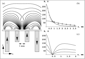
An interesting tool is a magnetic atom mirror formed by alternating magnetic dipoles (Opat et al., 1992), creating an exponentially growing field strength as the mirror is approached. This situation can be achieved by running alternating currents in an array of many parallel wires or by writing alternating magnetic domains into a magnetic medium such as a hard disk or a video tape. This has been demonstrated by Saba et al. (1999) and may achieve a periodicity in the order of 100nm. Current carrying structures have the disadvantage of large heat dissipation, especially when the structure size is in the submicron region.
Another possibility is based on a combination of current carrying wires and magnetic materials and was experimentally demonstrated at Harvard in the group of M. Prentiss: Two pairs of ferromagnetic foils that were magnetized by current carrying wires wound around them were used for magnetic and magnetooptic trapping (Vengalattore et al., 2001). The setup and the potential achieved is illustrated in Fig. 11. The advantages of such a hybrid scheme over a purely current carrying structure are larger capturing volumes of the traps, less heat dissipation, and enhanced trap depths and gradients because the magnetic field of the wires is greatly amplified by the magnetic material. The magnets can still be switched by means of time dependent currents through the wires.
II.2 Electric interaction
The interaction between a neutral atom and an electric field is determined by the electric polarizability of the atom. In general, is a tensor. For the simple atoms we consider, i.e. atoms with only one unpaired electron in an s-state, the electric polarizability is a scalar and the interaction can be written as
| (11) |
II.2.1 Interaction between a neutral atom and a charged wire
We now consider the interaction of a neutral polarizable atom with a charged wire (line charge ) inside a cylindrical ground plate (Hau et al., 1992; Schmiedmayer, 1995a; Denschlag and Schmiedmayer, 1997; Denschlag et al., 1998).
The interaction potential (in cylindrical coordinates) given by
| (12) |
is attractive. It has exactly the same radial form () as the centrifugal potential barrier () created by an angular momentum . is repulsive. The total Hamiltonian for the radial motion is
| (13) | |||||
| (14) |
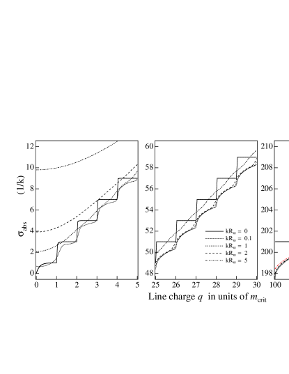
where is the critical angular momentum characteristic for the strength of the electric interaction. There are no stable orbits for the atom around the wire. Depending on whether is greater or smaller than , the atom either falls into the center and hits the wire () or escapes from the wire towards infinity (). In the quantum regime, only partial waves with ( is the quantum number of the angular momentum ) fall towards the singularity and thus the absorption cross section of the wire should be quantized (Fig. 12).
To build stable traps and guides one has to compensate the strongly attractive singular potential of the charged wire. This can be done either by adding a repulsive potential, for example from an atom mirror or an evanescent wave (see section II.3.1), or by oscillating electric fields (see section II.2.2).
II.2.2 Stabilizing the motion with an oscillating electric charge: the Kapitza wire
The motion in the attractive electric potential can be stabilized by oscillating the charges. The mechanism is similar to the RF Paul trap (Paul, 1990) where an oscillatory part of the electric fields creates a 3-dimensional confinement for ions. An elementary theoretical discussion of the motion in a sinusoidally varying potential shows that Newton’s equations of motion can then be integrated approximately, yielding a solution that consists of a fast oscillatory component superimposed on a slow motion that is governed by an effective potential (Landau and Lifshitz, 1976).
An example of a 2-dimensional atom trap based on a charged wire with oscillating charge was proposed by Hau et al. (1992). By sinusoidally varying the charge on a wire, it is possible to add an effective repulsive potential which stabilizes the motion of the atoms around the wire. Sizeable electrical currents appear when the charge of a real wire (with capacitance) is rapidly varied. Magnetic fields are produced which interact with the magnetic moment of an atom. This leads to additional potentials which have not been taken into account in the original calculations.
Another AC-electrical trap with several charged wires was proposed by Shimizu and Morinaga (1992). Their setup is reminiscent of a quadrupole mass filter and consists of 4 to 6 charged electrodes that are grouped around the trapping center. The atom experiences an oscillatory micromotion synchronous with the oscillation of the quadrupole potential, which leads to an overall trapping force.
II.2.3 Guiding atoms with a charged optical fiber

Stable orbits for the motion of an atom around a line charge are obtained if the atom is prevented from hitting the wire by a strong repulsive potential near the surface of the wire. Such a strong repulsion can be obtained by the exponential light shift potential of an evanescent wave that is blue detuned from an atomic resonance. This can be realized by replacing the wire with a charged optical fiber with the cladding removed and the blue detuned light propagating in the fiber (Batelaan et al., 1994). The fiber itself has to be conducting or coated with a thin () conducting layer to allow uniform charging. For the simple case of a TE01 mode propagating in the fiber, the light shift potential is independent of the polar angle and the combined guiding potential is given by:
| (15) |
where and are constants that depend on specifics of the optical fiber as well as on light power, wavelength and atomic properties (Batelaan et al., 1994). is the modified Bessel function of the second kind. Fig. 13 shows a typical example of such a potential. Cold atoms are bound in radial direction by the effective potential but free along the z-direction, the direction of the charged optical fiber.
II.3 Traps and guides formed by combining the interactions
II.3.1 Charged wire on a mirror
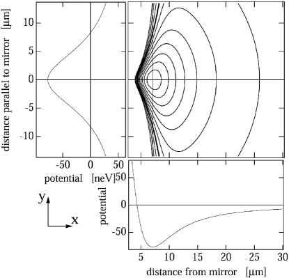
As we have seen previously, a static charged wire alone cannot form the basis for stable trapping. Cylindrical solutions such as the charged light fiber have the disadvantage that they cannot be mounted on a surface. An alternative solution would be to mount a charged wire onto the surface of an atom mirror. The combination of the attractive potential with the repulsive potential of the atom mirror888There are two main types of atom mirrors: The first type utilizes evanescent waves (e.g. above the surface of a reflecting prism) of blue detuned light which repels the atoms. Here the potential takes the form where is of the order of the light wave number and the distance from the mirror (Cook and Hill, 1982). The second type is based on a surface with alternating magnetic fields. Here, is the periodicity of the alternating magnetic field. The approaching atom experiences an exponentially increasing field, and consequently the weak field seekers are repelled (Opat et al., 1992; Roach et al., 1995; Sidorov et al., 1996; Hinds and Hughes, 1999) gives:
| (16) |
where is the height above the mirror and the distance from the wire. This creates a potential tube for the atoms as shown in Fig. 14 which can be viewed as a wave guide for neutral atoms.
Typical parameters for guides formed by a magnetic mirror and a charged wire are given by Schmiedmayer (1998). They can be very similar to the magnetic guides discussed in section II.1. Using typical mirror parameters (Roach et al., 1995; Sidorov et al., 1996), one can easily achieve deep and narrow guides with transverse level spacings in the kHz range for both light (Li) and heavy (Rb) atoms.
In a similar fashion microscopic traps can be created by mounting a charged tip (point) at or close beneath the atom mirror surface. A point charge on the surface of an atom mirror creates an attractive interaction potential:
| (17) |
where q is the tip charge. Together with the atomic mirror it forms a microscopic cell for the atoms. It can be viewed as the atom optical analog to a quantum dot (Schmiedmayer, 1998; Sekatskii et al., 2001).
This approach of combining a charged structure with an atom mirror is compatible with well developed nanofabrication techniques. This opens up a wide variety of possibilities ranging from curved and split guides to interferometers or even complex networks.
II.3.2 Combined electric-magnetic state dependent traps
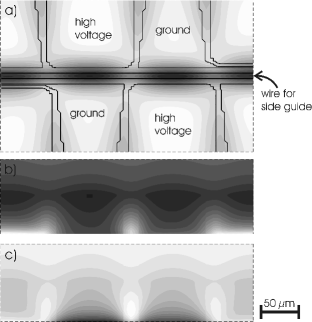
The magnetic guides and traps (section II.1) can be modified by combining them with the electric interaction, thereby creating tailored potentials depending on internal (e.g. spin) states. For example, supplementary electrodes located between independent magnetic traps can be used to lower the magnetic barrier between them by the attractive electric potential the electrodes create. Since the magnetic barrier height depends on the magnetic substate of the atom, whereas the electric potential does not, this allows state selective operation. This is especially interesting since it can lead to implementing quantum information processing with neutral atoms in microscopic trapping potentials where the logical states are identified with atomic internal levels (see section VI).
A simple example, showing such a controllable state dependence, is a magnetic wire guide approached by a set of electrodes (Fig. 15a). Applying a high voltage to the electrodes introduces an electrostatic potential which provides confinement along the direction parallel to the magnetic side guide, and also shifts the trapping minimum towards the surface, possibly breaking the magnetic potential barrier in the direction perpendicular to the surface itself. The charge can be adjusted in a way that depending on the strength of the magnetic barrier created by the wire current, the atoms either impact onto the surface or are trapped above it. Since the strength of the magnetic barrier depends on the magnetic substate of the atom or, more precisely, depends linearly on the quantum number , this can be exploited to form a state selective magnetic trap (Fig. 15b,c).
II.3.3 The electric motor
In general, electric fields are always present in magnetic wire traps since an electric potential difference is needed to drive a current through a wire with finite resistance. For large wires, the voltages in question are low and if the distances of the atoms from the wire are large enough, the attractive electric interaction can be neglected. However, for micron sized wires, one finds that if the current carrying wire becomes long, at some point the voltage is strong enough to create a significant driving force for the atoms or even to destroy the traps.
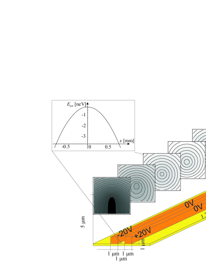
On the other hand, one can actually exploit this effect and turn it into an ‘electric motor’ by using the electric potential gradient inside the magnetic minimum to accelerate and decelerate the atoms at will. Fig. 16 illustrates the mechanism used for the motor for the example of a two wire guide with a vertical bias field. The wires carry counter-propagating currents, and the polarization interaction is zero in the middle of the guide (see inset) where both wires have the same voltage. By adding a homogeneous electric potential relative to ground, the zero electric field point may be moved at will to achieve any acceleration or deceleration rate. A constant acceleration is obtained when the zero electric field point is maintained at a constant distance from the position of the atoms.
II.4 Miniaturization and technological considerations
To achieve very robust and highly controlled atom manipulation one would like to localize atoms in steep traps or guides which can be fabricated with high precision. The large technological advances in precise nanofabrication, with the achievable size limit on chips smaller than 100nm, makes the adaptation of these processes for mounting the wires onto surfaces very attractive.
II.4.1 Miniaturization
The main motivations behind miniaturization and surface fabrication are:
-
•
Large trap level spacings help to suppress heating rates. To achieve the necessary large trapping gradients and curvatures with reasonable power consumption, miniaturization is unavoidable (see section II.4.4).
-
•
The tailoring resolution of the potentials used for atom manipulation is given by the resolution of the fabrication of the structures used. It is, for example, important for the realization of atom–atom entanglement by controlled collisions as suggested by Calarco et al. (2000)(see section VI) to reduce the distances between individual trapping sites to the micron regime. This would be virtually impossible with (large) free standing structures.
-
•
Nanofabrication is a mature field which allows one to place wires on a surface with great accuracy (nm). Surface mounted structures are very robust and the substrate serves as a heat sink allowing larger current densities (see section II.4.4). In addition, nanofabrication allows parallelism in production of manipulating elements (scalability).
-
•
Nanofabrication also allows us to contemplate the integration of other techniques on the chip (see section VI for details).
II.4.2 Finite size effects
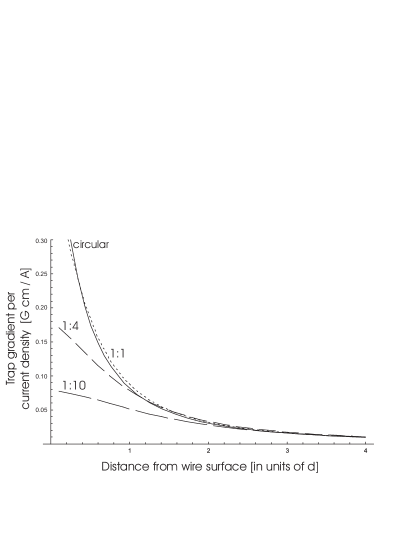
The formulae presented in section II.1 to II.3 are exact only for infinitely small wire cross sections. In the case of a physical wire with a finite cross section, they are a good approximation only as long as the height above the wire is greater than the width of the wire. For experiments requiring a trap height smaller than the width of the wire, finite size effects have to be taken into account. In Fig. 17, we present examples of numerical calculations showing how the trap gradient is limited by finite size wires. One clearly sees that at trap heights in the order of the width of the wire the resulting gradient starts to deviate from the expected value. The effect is small for wires with a square cross section, while it becomes considerably more important when rectangular wires with high ratios of width to thickness are used.
II.4.3 Van der Waals interaction
The Van der Waals interaction becomes important at distances of the order of a few 100nm from the surface. The interaction can be strong enough to significantly alter the magnetic and electric trapping potentials (Grimm et al., 2000). Traps much closer than 100nm from the surface will be very hard to achieve since the Van der Waals potential attracts the atoms to the surface and increases with (in the non-retarded regime where the distance is smaller than the optical wavelength).
II.4.4 Current densities
A limiting factor in creating steep traps and guides is the maximally tolerable current density of a current carrying structure. Considering a side guide potential created by a wire with finite width and a constant thickness, the highest possible gradient is achieved at a distance from the wire comparable with . The bias field needed for such a trap is given by the ratio of the maximum current that can be pushed through the wire and ; therefore the bias field is proportional to the maximum current density . This leads to the conclusion that the highest possible gradient is given by which favors smaller wires. If a square wire cross section is assumed, the maximum gradient is proportional to . Even in this case, smaller will allow for larger gradients because has been observed to increase with smaller wire cross sections. The drive for smaller width is stopped at a distance of about 100nm where surface decoherence effects (see section V) and Van der Waals forces may be too strong to endure. Hence, it is probably of no use to make the wires even thinner.
II.4.5 Multi-layer chips
Last, one should also note that as more complex operations are demanded from the atom chip (see section VI), it will have to move on from a 2-dimensional structure into a 3-dimensional structure in which not only current and charge carrying wires are embedded, but also light elements and wave guides. These highly complex devices will force upon the fabrication a whole range of material and geometrical constraints.
III Experiments with free standing structures
The basic principles of microscopic atom optics have been demonstrated using free standing structures: current carrying and charged wires. The interaction potentials are in general shallow, typically only a few mK deep. Hence experiments use cold atoms from a MOT or a well collimated atom beam (even the moderate collimation of 1mm over 1m results in a typical transverse temperature of mK).
Free standing wire structures can be installed close to a standard six beam MOT without significantly disturbing its operation (as long as the wire is thin enough), and offer large optical access which has advantages when probing the dynamics of the atoms and their spatial distribution within the wire potentials. They have the disadvantages that they are not very sturdy, they deform easily due to external forces, and they cannot be cooled efficiently to dissipate energy from ohmic heating. This limits the achievable confinement and the potential complexity of wire networks. Nevertheless there are some special potentials which can only be realized with free standing wires.
III.1 Magnetic interaction
As discussed in section II.1 there are two possibilities for magnetically trapping a particle with a magnetic moment: traps for strong field seekers and traps for weak field seekers. In the following we describe experiments with magnetic microtraps which are based on small, free standing wires or other magnetic structures. Typical wire sizes range from 10m to a few of mm and the wires carry electrical currents of up to 20A. All experiments but the first example start with a conventional MOT of alkali atoms (lithium or rubidium) which is initially situated a few mm away from the magnetic field producing structures. This distance prevents the atoms in the MOT from coming into contact with the structure surface where they would be absorbed. It also provides the necessary optical access for the MOT laser beams.
To load the magnetic wire traps and guides, the MOT laser light is simply switched off and the magnetic trap fields are turned on. The loading rate into the miniature magnetic traps has been enhanced in some experiments a) by optically pumping the unpolarized MOT atoms to the right trapping state (Key et al., 2000); b) by first loading the MOT atoms in a size matched magnetic trap which is then further adiabatically compressed (Vuletic et al., 1996, 1998; Key et al., 2000; Fortagh et al., 1998; Haase et al., 2001); c) by moving the MOT closer to the trapping region shortly before the light is turned off which can be done with an additional magnetic bias field (Denschlag et al., 1999a). In this way the efficiency of transferring the atoms into the miniature magnetic traps reached between 1 and 40 %. In general the spatial distribution of the trapped atoms was imaged with a CCD camera by shining a resonant laser beam onto the atoms and detecting its absorption or the atomic fluorescence.
III.1.1 Magnetic strong field seeking traps: the Kepler guide
A magnetic strong field seeker trap for cold neutral atoms was experimentally demonstrated in two experiments: in 1991 by guiding an effusive beam of thermal sodium atoms (mean velocity 600m/s) along a m long current carrying wire (Schmiedmayer, 1992, 1995a, 1995b) and in 1998 with cold lithium atoms loaded from a MOT (Denschlag et al., 1999a).
The experimental setup for the beam experiment is given in Fig. 18. The atom beam is emitted from a 1mm-diameter nozzle in a 100∘C oven and is collimated to 3mrad. Introducing a small bend in the wire (mrad), one can guide some of the atoms along the wire around the beam stop. The atomic flux was measured with a hot wire detector. The guiding wire was 150m thick and carried 2A of electrical current.
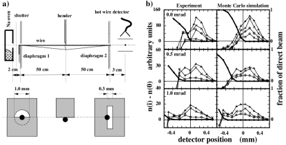
In the second experiment, lithium atoms were cooled in a MOT (1.6mm diameter FWHM) to about 200K (which corresponds to a velocity of about 0.5 m/s). By shifting the MOT onto a 50m thick wire and releasing the atoms from the MOT, about 10 of the unpolarized atomic gas could magnetically be trapped in orbits of about 1mm diameter around the wire that carried about 1A of current. Monte Carlo calculations indicate that by optically pumping the atoms and optimizing the trap size and current through the wire, it should be possible to guide over 40% of the atoms from a thermal cloud with the Kepler guide. The loading efficiency is limited to this amount, because atoms in highly eccentric orbits hit the wire and are lost.
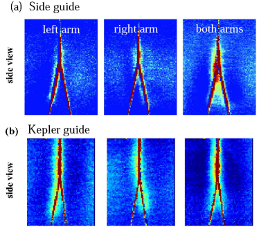
The bound atoms are guided along the wire corresponding to their initial velocity component in this direction. Consequently a cylindrical atomic cloud forms that expands along the wire. After 40ms of guiding, the atoms typically had propagated over a 2cm distance along the wire (see Fig. 19 (left)). For long guiding times the bound atoms leave the field of view, and the fluorescence signal of the atoms decreases. The top view images of Fig. 19 (left) show a round atom cloud that is centered on the wire suggesting that atoms circle around it.
By studying the ballistic expansion of the bound atoms after switching off the guiding potentials, the momentum distribution of the guided atoms can be extracted. Fig. 19(center) shows a picture sequence demonstrating how the atomic cloud expands as a function of time. Starting from a well localized cylindrical cloud of guided atoms at t = 0 the spatial atomic distribution transforms into a doughnut-like shape. This shows that there are no zero-velocity atoms in the Kepler guide. In order to be trapped in stable orbits around the wire the atoms need sufficient angular momentum and therefore velocity. Atoms with too little angular momentum hit the wire and are lost.

Guiding in the Kepler guide is very sensitive to the presence of uncompensated bias fields. Such additional magnetic bias fields, even if homogeneous, destroy the rotational symmetry of the Kepler potential and angular momentum is not conserved anymore. Over the course of time, the Kepler orbits become increasingly eccentric and thus finally hit the current carrying wire leading to loss, which was confirmed by Monte Carlo calculations. The right side of Fig. 19 shows a qualitative experiment investigating the dependence of the magnetic trap stability on the magnetic bias field. The remaining atom number in the Kepler guide was measured after 20ms of interaction time. It clearly decreases with increasing bias field strength: the larger the bias field, the faster the atoms get lost (Denschlag, 1998). In a case of a weak disturbance the orbits can be stabilized by an additional potential which leads to a precession of the orbits.
III.1.2 Magnetic weak field seeking traps and guides
The development of miniature weak field seeker traps, as discussed in Section II.1.2 and II.1.3, lays the foundations for microscopic atom optics. Here and in the following sections we restrict our discussion explicitly to experiments with free standing structures. Surface mounted guides and traps are discussed in Section IV.
In the following experiments the circular symmetric magnetic field of a straight current carrying wire is combined with a magnetic bias field as described in Section II.1.2. The two fields cancel each other along a line that is parallel to the wire creating a magnetic field minimum (side guide). In the simplest case, the bias field can be created by an additional wire (Fig. 20a) (Fortagh et al., 1998) or by an homogeneous external field (Fig. 20b) (Denschlag, 1998; Denschlag et al., 1999a). Four wires also create a 2-dimensional quadrupole field (Fig. 20c) (Key et al., 2000).
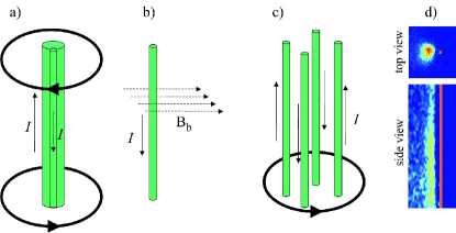
The experiments of the group of C. Zimmermann (Fortagh et al., 1998) used additional endcap (‘pinch’) coils (see Fig. 20a) to confine the atoms also in the direction along the wire. They succeeded in adiabatically transferring and compressing the magnetic trap - reaching a relatively high transfer efficiency of 14% from the MOT into a microtrap without losing in phase space density. In experiments in Innsbruck (Denschlag, 1998; Denschlag et al., 1999a) and Sussex (Key et al., 2000) (Figs. 20b and c, respectively) cold atoms released from a MOT were guided along the wires a distance of one to two centimeters (Fig. 20d). In addition the vertical Sussex experiment used one bottom pinch coil to confine the falling atoms from exiting the guide. The atoms bounced back and were imaged at the top exit.
By choosing appropriate bias field strengths and wire currents, a wide range of traps with different gradients have been realized and the interesting scaling properties (see section II.1.4) were studied. With a fixed trap depth (given by the magnitude of the bias field ) the trap size and its distance from the wire can be controlled by the current in the wire. The trap gets smaller and steeper (gradient ) for decreasing the current in the wire, which was confirmed experimentally (Denschlag, 1998; Denschlag et al., 1999a). For example, a trap with a gradient over 1000G/cm can be achieved with a moderate current of A and an offset field of G. The trap is then be located m away from the wire center.
A different interesting low field seeker trap has been experimentally realized by placing a current carrying wire right through the minimum of a magnetic quadrupole field (Denschlag, 1998; Denschlag et al., 1999b). If the wire is aligned along the direction of the symmetry axis of the quadrupole field a ring shaped potential is obtained with a non-vanishing minimum field strength (see section II.1.4 and Fig. 5d).
III.1.3 Beam splitters
Although free-standing wire experiments are certainly limited in their architectural complexity because of mechanical stability, some variations of the straight wire geometry have been explored. By combining two free standing wires one can form a “Y” or fork, which can be used as an atomic switch (see Fig. 21) (Cassettari et al., 1998; Denschlag et al., 1999b). Choosing an arm of the fork through which an electrical current is conducted, the atomic flow can be switched from one arm to the other. If current is sent through both arms the atom beam is split in two.
III.1.4 Free-standing bent wire traps
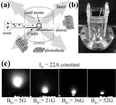
Experiments with free standing wires that are bent in shape of a “U” or “Z” have been reported by Denschlag et al. (1999b); Haase (2000); Haase et al. (2001). Bending the wire has the effect of putting potential endcaps on the wire guide, which turns it into a 3-dimensional low field seeker trap. As explained in detail in section II, in the “U” case a quadrupole trap is formed and for the Z-configuration the trap is of the Ioffe-Pritchard type. Such a Z-wire trap can achieve trapping parameters similar to the ones currently used in conventional BEC production, here, however, with moderate currents of a few amperes. In their experiment, Haase et al. used a 1mm thick copper wire, with the central bar being about 6mm long. The wire can carry 25A without any sign of heating. Fig. 22c shows the scaling properties of the Z-trap. The atomic cloud can be compressed by raising the bias field or by lowering the wire current.
III.1.5 The tip trap

Vuletic et al. (1996, 1998) have demonstrated a miniature magnetic quadrupole trap (the tip trap) by mounting small coils on a combination of permanent magnets and ferromagnetic pole pieces (see Fig. 23). In this way they exploited the fact that for a given magnetic field the maximum possible field gradient scales like where R is the geometric size of the smallest relevant element. The central element of the tip trap is a 0.65mm steel pin of which one tip is sharpened to a radius of curvature of 10m. Thus with m and G the magnetic field gradient exceeded G/cm. Working with lithium atoms, this gradient implies a ground state size of the atomic wavefunction smaller than the wavelength of the optical transition at 671nm. The microtrap was loaded by adiabatic transport and compression: The atoms of the lithium MOT are transferred to a volume matched, but still relatively shallow magnetic potential after turning off the MOT light. By adiabatically changing the currents through the miniature coils the magnetic trap compresses its size by a factor of 6.5 within 100ms. A total of 3% of the MOT atoms could be transferred to the microtrap at moderate currents of 3A through the tip trap coils.
III.1.6 Scattering experiments with a current carrying wire
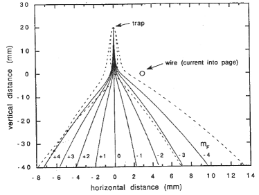
In 1995 the Melbourne group (Rowlands et al., 1995; Rowlands et al., 1996a, b) performed an experiment where a beam of laser cooled cesium atoms, after being released from a MOT, is scattered off a current carrying wire. As the atoms pass through the static inhomogeneous magnetic field of the wire they are deflected by a force dependent on the magnetic substate of the atom (see Fig. 24). With currents of up to 45A through the wire, the positions of the atoms in the individual magnetic substates are resolved and deflection angles as large as 25∘ are observed. State preparation of the atoms using optical pumping increases the number of atoms deflected through essentially the same angle.
III.1.7 A storage ring for neutral atoms
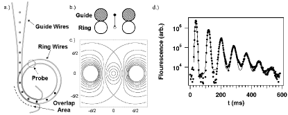
Very recently Sauer et al. (2001) have demonstrated a storage ring for neutral atoms using a two wire guide (section II.1.3). A pair of wires (separation m) which forms a ring of 2cm diameter, produces a 2-dimensional quadrupole magnetic field (see Fig. 25). The wires carry currents of 8A in the same direction which produces a field minimum between the two wires with a field gradient of 1800G/cm and a trap depth of 2.5 mK for the ground state of 87Rb (weak field seeker). The ring has a diameter of 2cm and is loaded from a MOT via a similar second two wire waveguide. The MOT is turned off and the second waveguide is ramped up in 5ms. Approximately laser cooled rubidium atoms (longitudinal temperature 3K) fall 4cm under gravity along the guide after which they enter the storage ring with a velocity of about 1m/s. To transfer the atoms to the ring, the current in the guide is ramped off while simultaneously increasing the current in the ring. Using fluorescence imaging the position and the number of the atom cloud can be probed. Up to seven revolutions of the atoms in the ring have been observed.
III.2 Charged wire experiments
Two types of experiments have used the potential (eq. 12) of a charged wire. One investigated the effect of a charged wire in atom interferometry. The other investigated atomic motion in the singularity of the potential. Here, laser cooled atoms fall into the attractive singularity and are lost as they hit the charged wire.
III.2.1 A charged wire and interferometry
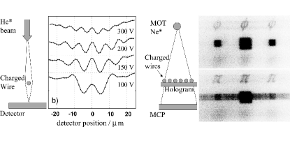
Shimizu et al. (1992) used a straight charged wire to shift (deflect) the interference patterns of a matter wave interferometer in a Young’s double slit configuration. In a recent experiment of the same group (Fujita et al., 2000) (Fig. 26 (right)), this work is expanded by combining a binary matter wave hologram with an array of straight charged wires. By changing the electric potential applied to the electrodes on the hologram the holographic image patterns can be shifted or erased, and it is even possible to switch between two arbitrary holographic image patterns999Similarly it was suggested by Ekstrom et al. (1992) that charged patches on a grating can be used to modify the diffraction properties.. These experiments were performed using laser cooled metastable neon in the 1s3 state. After releasing them from the MOT, the atoms fell under gravity onto a double slit or a binary hologram. A few centimeters further down the atoms formed an interference pattern which was detected by a multi-channel plate (MCP).
The binary hologram pattern held an array of 513 regularly spaced parallel wires of platinum on its surface. Each electrode was either grounded or connected to a terminal. The width and the spacing of each wire was 0.5m and the holes for the binary hologram in between the wires were 0.5m 0.5m in size. The electric field generated between two wires shifted the energy of the neon atom by . When two adjacent electrodes had the same potential, the atoms in the gap were unaffected. If they had different potentials, the atoms accumulated an additional phase while passing through the hole.
In an experiment in Konstanz, Nowak et al. (1998) sent a collimated thermal beam of metastable helium atoms onto a charged wire (tungsten, 4 m diameter) where it was diffracted (see Fig. 26 (left)). 1.3m further downstream they observed an interferometric fringe pattern which depended on the wire charge and on the de Broglie wavelength. The data agreed well with the theoretical predictions for scattering polarizable particles off a potential.
III.2.2 A charged wire in gas of cold atoms: studying a singular potential
The motion in a singularity can be studied by placing a cloud of cold atoms in the potential of a charged wire. In this experiment the number of cold lithium atoms of a MOT is monitored while the atoms move in the potential of the wire (Denschlag et al., 1998). At extremely low light levels the MOT acts as a box holding a gas of atoms. Atoms falling into the attractive singularity are lost as they hit the wire. This loss mechanism leads to an exponential decay of the trapped atom number (see Fig. 27b).
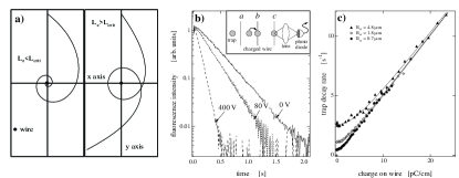
The corresponding loss rate is characteristic for the singularity and its strength. Atoms with angular momentum (see Eq. (14) in section II.2) fall into the singularity. The loss rate is a linear function of because is proportional to the line charge and the atoms are uniformly distributed over angular momentum states (see Fig. 27c). This is actually true only for high charges, since for lower , the finite thickness of the charged wire becomes apparent. The MOT decay rate for an uncharged wire is proportional to its actual diameter. The diameters of the wires in the experiments ranged between 0.7m and 5m. A detailed analysis of the absorption data reveals that Van der Waals forces also contribute to the atomic absorption rate (Denschlag, 1998). This effect was found to be important for thin wires with diameters of less than 1m. Hence this system should allow for detailed future studies of Van der Waals interaction and retardation in nontrivial boundary conditions.
The potential would be especially interesting to study in the quantum regime where the de Broglie wavelength of the atoms is much larger than the diameter of the charged wire; the quantization of angular momentum then begins to play a role (Denschlag and Schmiedmayer, 1997). This can be used for example in order to build an angular momentum filter for atoms (Schmiedmayer, 1995a).
IV Surface mounted structures: The atom chip
Free standing structures, as those described in the previous section, are extremely delicate, and one arrives quickly at their structural limit, when miniaturizing traps and guides. Wires mounted on a surface are more robust, can be made much smaller and heat is dissipated more easily which allows significantly more current density to be sent through the wires. This together with strong bias fields allows for tighter confinement of atoms in the traps. Consequently, ground state sizes nm become feasible. Existing accurate nanofabrication technology provides rich and well established production procedures, not only for conducting structures, but also for micromagnets. Optical elements such as microoptics, photonic crystals and microcavities can also be included to arrive at a highly integrated device. The small ground state size of such microtraps implies that we know the exact location of the atom relative to other structures on the surface to the precision of the fabrication process (typically nm), allowing extremely close sites to be addressed individually for manipulation and measurement.
We have named nanofabricated surfaces for cold atom manipulation ‘atom chips’ in reminder of the similarity of these atom optical circuits to electronic integrated circuits. In designing atom chips one attempts to bring together the best of two worlds: the well developed techniques of quantum manipulation of atoms, and the mature world of nanofabrication in electronics and optics, to build complex experiments utilizing the above techniques.
In the following we describe the atom chip and its present experimental status. Future goals will be addressed in section VI.
IV.1 Fabrication
There are many different techniques of atom manipulation which can be integrated into an atom chip. Present atom chip experiments follow a simple scheme based on wires that carry currents or charges. These allow to miniaturize the free standing devices discussed in section III. We will focus here on these simple integrated structures, leaving issues of further integration to the outlook in section VI.
To build an atom chip one has to solve the following problems: first of all, the microstructures have to withstand high current densities and high electric fields. This requires structures with low electrical resistance and good heat conductivity. The material of choice for the wires is gold, though other materials such as copper are also used. For the substrate one wants good heat conductivity with high electrical insulation withstanding large electric fields (created at sharp (m) corners even by small voltages), and ease of fabrication. Typical materials are silicon, gallium arsenide, aluminum nitride, aluminum oxide and sapphire (), though glass has also been used.
Another requirement lies in the fact that cold atoms have to be collected and then transferred towards the small traps on the chip. If one wants to avoid transferring the atoms from a distant MOT, the chip has to be either transparent or reflecting, to allow lasers to address the atoms from all directions near the surface. Nevertheless, experiments exist in which the atoms have been brought from a distance to a chip (Ott et al., 2001; Gustavson et al., 2001).
Presently, atom chips are built mainly using two technologies: thin film hybrid technology, or plain nanofabrication which is the first step of the two stage hybrid technology.
IV.1.1 Thin film hybrid technology
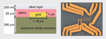
In this approach one starts from an insulating substrate (e.g. sapphire) and patterns, using lithographic techniques, a layout of the desired structure onto a thin (nm) metallic layer. In the second stage, the wires are grown by electroplating: Metal ions from a solution are deposited onto the exposed metallic layer, which is now charged. With this process one obtains wires with quite large cross sections (typical structure widths are to m) that support high currents. However, miniaturization will be limited to a few micron wire width. Furthermore, surface roughness is quite large, which makes such surfaces less suitable for the reflection MOT and atom detection. These drawbacks and the expected shadows from large etchings between wires, have been dealt with successfully by covering the chip with an insulating layer and then with a metallic reflection layer e.g., with the Munich chip as shown in Fig. 28) (Reichel et al., 2001). This, however, carries the price of not enabling atoms to be closer than some m from the wires themselves. A technical advantage of electroplating is that it wastes less gold because one avoids evaporation of large amounts of gold, which mostly cover the evaporation chamber and not the chip.
Atom chips fabricated using using this technique have been used sucessfully by the groups in Harvard (M. Prentiss), Munich (J. Reichel and T. W. Hänsch), JILA, Boulder (D. Anderson and E. Cornell) and Tübingen (C. Zimmermann).
IV.1.2 Nanofabrication
Atom chip structures can also be fabricated into an evaporated conductive layer with state–of–the–art processes used for electronic chips. To the best of our knowledge, this approach is only used by the Heidelberg (formerly Innsbruck) group. In these atom chips a m gold layer is evaporated onto a mm thick semiconductor substrate (GaAs or Si). As GaAs or Si tend to leak current, especially in the presence of light, a thin isolating layer of is put between the substrate and the gold layer. The chip wires are defined by m wide etchings from which the conductive gold has been removed. This leaves the chip as a gold mirror that can be used to reflect MOT laser beams (the m etchings impede the MOT operation only in a slight way). The mirror surface quality is very high, achieving an extremely low amount of scattered light. The chips were produced at the microfabrication centers of the University of Vienna and of the Weizmann Institute of Science (Rehovot), see Fig. 29.
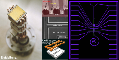
Atom chips fabricated with this method have the advantage that the structure size is only limited by nanofabrication (nm). The drawback is that the conductive layer cannot be too thick. This is due mainly to restrictions on the available thickness of the photoresist used in the process. The thin wires support only smaller currents, and therefore only smaller traps closer to the surface can be built. This disadvantage can be corrected by adding larger wires below the chip surface, as presented in Fig. 29.
At this stage it is hard to judge what is the best fabrication process. There are still many open questions. For example, is there a sizable difference in the specific resistance between evaporated gold and electroplated gold? For a direct comparison, one would have to unify all other parameters such as substrates and intermediate layers. Another question concerns the final fabrication resolution one wishes to realize. Assuming one aspires to achieve the smallest possible trap height above the chip surface for sake of low power consumption and high potential tailoring resolution, the limit will be at a height below which surface induced decoherence becomes too strong (see sec. V). This height, together with the finite size effects described in section II, will determine the fabrication resolution needed. Smoothness of resolution will also be required as fluctuating wire widths will change the current density and therefore the trap frequency in a way that may hinder the transport of BEC due to potential hills. Finally, as multi–layer chips using more elaborate 3-dimensional designs are introduced e.g. for wire crossings and more complicated structures including photonic elements, it may be that conductor layers thicker than a few microns will have to be abandoned. In order to fully exploit the potential of the atom chip in the future, the technology used will have to be such that all elements could be made with a suitable process into a monolithic device.
Finally, we note that although usual current densities used in the experiments range between A/cm2 (higher with smaller cross sections and depending on pulse time, work cycle and heat conductivity of substrate), densities of up to A/cm2 have been reported for cooled substrates (Drndić et al., 1998). Gold wires have been found to be the best, achieving superior performance even when compared to superconductors.
IV.2 Loading the chip
In general there are two different approaches to loading cold atoms into the chip traps:
(i) Collect and cool the atoms at a different location and transport the cold ensemble to the surface traps. This may be achieved using direct injection from a cold atomic beam coming from a low–velocity–intense–source (LVIS) (Müller et al., 1999, 2000, 2001) or a released MOT whereby the atoms are pulled by gravity (Dekker et al., 2000). Transferring the atoms with magnetic traps has also been achieved (Ott et al., 2001). Experiments transferring a Bose–Einstein condensate (BEC) using optical tweezers also exist (Gustavson et al., 2001).
(ii) Cool and trap atoms close to the surface in a surface MOT, and transfer the atoms from there to the microtraps on the chip (Reichel et al., 1999; Folman et al., 2000). For this method to be implemented, a MOT has to be formed close to the surface, and consequently the atom chip has either to be transparent or reflecting.
In the following, we describe experiments performed at Heidelberg (resp. Innsbruck), Sussex and Munich using the second approach. Further on, several experiments using the first approach will also be discussed (e.g. Figs. 37 and 38).
IV.2.1 Mirror MOT
The first problem to solve is how to obtain a MOT configuration close to a surface. This problem has an easy solution if we recall that a circularly polarized light beam changes helicity upon reflection from a mirror. To the best of our knowledge, this idea was first put into practice with a pyramid of mirrors and one beam (Lee et al., 1996), as presented in Fig. 30a. Almost in parallel, a single planar surface with four beams impinging at degrees onto the surface was used, thus realizing an eight beam MOT (Pfau et al., 1997; Schneble et al., 1999; Gauck et al., 1998; Schneble et al., 2001) 101010It is interesting to note that in another version of this experiment, an evanescent field just above the extremely thin metal surface, formed by light beams impinging on the back of the surface, was used as an atom mirror. This allowed to produce a MOT with reasonable surface induced losses even at the extreme proximity of nm from the surface.. In the surface MOT most common today one generates the MOT beam configuration from four beams by reflecting only two beams off the chip surface (see Fig. 30b) (Reichel et al., 1999; Folman et al., 2000).

The magnetic quadrupole field for the MOT can be obtained either by a set of external quadrupole coils, or by superimposing a homogeneous bias field with the field generated from a U–shaped wire on or below the chip (‘U–MOT’). External quadrupole coils generate the correct magnetic field configuration if one of the reflected light beams is in the coil axis. If the U–MOT is used, the reflected light beams must lie in the symmetry plane of the U. Trapping in the U–MOT has the advantage that the MOT is well aligned with respect to the chip and its microtraps. If the mirror MOT is sufficiently far from the surface (a few times the MOT radius), its loading rate and final atom number are very similar to a regular free space MOT under the same conditions (laser power, vacuum, supply of cold atoms, etc.). In agreement with earlier observations using wires, the shadows (diffraction patterns) from the m etchings in the gold surface of the nanofabricated atom chip do not disturb the MOT significantly (Denschlag et al., 1999a; Denschlag, 1998).
Such atom chip mirror MOTs, have been loaded from an atomic beam in Innsbruck/Heidelberg (Folman et al., 2000), from the background vapor in Munich (Reichel et al., 1999) and in a double MOT system in Innsbruck/Heidelberg ( atoms at lifetime s), using either external coils or the U–wire for the quadrupole field. In addition, at Sussex and Harvard surface MOTs were realized using permanent and semi-permanent (magnetizable cores) magnetic structures.
As an example we describe the Innsbruck/Heidelberg lithium setup. Fig. 31 shows a top view of the mirror MOT sitting above the chip with some of its electric connections. For the transfer into the U–MOT, the large external quadrupole coils are switched off while the current in the U–shaped wire underneath the chip is switched on (up to A), together with an external bias field (G). This forms a nearly identical, but spatially smaller quadrupole field as compared to the fields of the large coils. By changing the bias field, the U–MOT can be compressed and shifted close to the chip surface (typically mm). The laser power and detuning are changed to further cool the atoms, giving a sample with a temperature of about K.
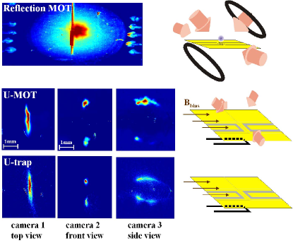
IV.2.2 Transferring atoms to the chip surface
After the U–MOT phase, atoms are cooled using optical molasses, optically pumped and transferred into a matched magnetic trap, typically produced by a thick Z-shaped wire plus bias field. From there atoms are transferred closer and closer to the chip and loaded sequentially into smaller and smaller traps. In general, it is favorable to lower the trap towards the surface by increasing the magnetic bias field. This way the trap depth increases and less atoms are lost due to adiabatic heating during compression. Unfortunately this is not feasible all the way: Finite size effects limit small traps to thin wires, at the price of not being able to push high currents.
The basic transfer principle from a large wire to a small wire is to switch on first the current for the smaller trap, and then to ramp down the current in the bigger trap maintained by a thicker wire (Fig. 32). Further compression is achieved by using smaller and smaller currents. Care has to be taken, that the transfer is adiabatic, especially with respect to the motion of the potential minimum. By an appropriate change of the bias field, the compression of the atoms in the shrinking trap can be performed very smoothly. Transferring into more complicated potential configurations one has to avoid the opening of escape routes for the trapped atoms.
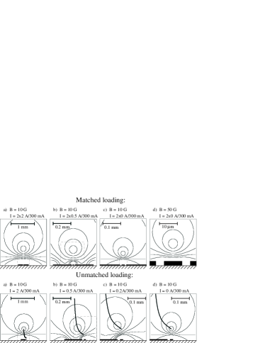
For an adiabatic transfer of relatively hot atoms, the main loss is due to heating: when compressing by lowering the current, high–lying levels may eventually spill over the potential barrier. Significant loss occurs if the trap depth is much smaller than times the temperature of the atomic ensemble. Other loss mechanisms are described in section V. For thermal clouds, typical achieved transfer efficiencies from the MOT to the magnetic chip trap are as high as .
As a detailed example we describe the loading of the first of the Innsbruck experiments (Folman et al., 2000). After accumulating atoms in a mirror MOT and transferring them to the U–MOT, the laser beams are switched off and the quadrupole field generated by the U–shaped wire below the chip surface serves as a magnetic trap for low–field seekers (Fig. 31: U–trap). The magnetic trap is lowered further towards the surface of the chip by increasing the bias field. Atoms are now close enough to be trapped by the chip fields. Next, a current of A is sent through two m U–shaped wires on the chip, and the current in the U–shaped wire located underneath the chip is ramped down to zero. This procedure brings the atoms closer to the chip, compresses the trap considerably, and transfers the atoms to a magnetic trap formed by the currents on the chip surface. This trap is further compressed and lowered towards the surface (typically m) by increasing the bias field (Fig. 33). From there the atoms are transferred to a microtrap created by a m Z–shaped wire.
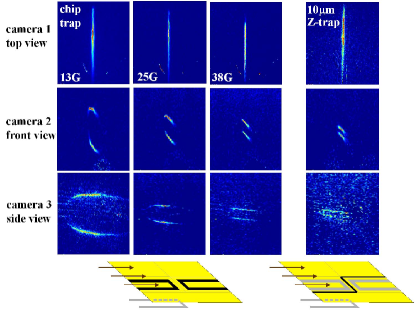
In the lowest height and most compressed trap achieved to date, a m2 Z–shaped wire is used with a current of mA (Heidelberg). With a bias field of G the atoms are trapped at a height of about m above the surface and at an angular oscillation frequency kHz (magnetic field gradients of kG/cm) for several tens of ms (see eq. 6 for typical trap frequencies). At such a small trap height several problems come into play: First, with the present mm distance between the bends of the Z–shaped wire, the Ioffe–Pritchard configuration is lost and one is left with a single wire quadrupole field where atoms can suffer Majorana flips. Two easy remedies would involve smaller Z lengths or a slight tilt of the bias field direction. Second, the trap is so tight that the number of atoms that survive the transfer and compression is small. This limitation should not be applicable in the case of a BEC as there are no high-lying states where atoms run the risk of spilling over the finite trap barrier. A third problem has to do with the observation of the atoms: even with negligible stray light from surface scattering or blurring by atomic motion, it is found that direct observation of extremely tight traps close to the surface (m) is very hard. The signal suppression is probably due to large Zeeman shifts in the cloud, which together with optical pumping processes dramatically reduce the scattered light. In such a case, one can observe the atoms after trapping by ‘pulling’ them up, away from the surface into a less compressed trap. This may be done simply by increasing the wire current or decreasing the bias field.
IV.2.3 Observing atoms on the chip
A simple way to observe the trapped atoms is by fluorescence imaging. For this, one illuminates the cloud with near–resonant molasses laser beams for a short time (typically much less than ms). The scattered light is imaged by CCD cameras as shown in Fig. 31 and Fig. 33. One should use short enough exposure times to avoid blurring of the image due to atomic motion. One also has to select the camera positions wisely to avoid stray light caused by scattering off the etchings in the atom chip surface. Furthermore, it is important that the metal surface itself shows minimal light scattering. Here, the excellent surface quality of evaporation on semiconductor surfaces is essential.
A different possibility is to use absorption or phase contrast imaging. If the probe beam is directed parallel to the chip surface, the surface quality is not as critical, and one does not have to take care of diffraction peaks from the etchings. Such absorption imaging is used by the Munich and Tübingen groups. With an excellent surface mirror quality, one could also implement absorption imaging with laser beams reflected from the chip surface. More sophisticated methods such as phase contrast imaging will be important for more complicated atom optical devices on atom chips, where non-destructive observation very close to the chip surface becomes essential. For an overview of these methods, we refer the reader to the many BEC review papers (see for example Ketterle (1999)).
Finally, future light optical elements incorporated on the chip, such as microspheres or cavities, will allow for much better detection sensitivity, possibly at the single atom level (see section VI.1.3). Such work has been started in several of the labs.
IV.3 Atom chip experiments
Since the first attempts two years ago, the atom chip has now become a ‘tool box in development’ in numerous labs around the world. To the best of our knowledge these include (in alphabetical order) the groups at Boulder/JILA (D. Anderson and E. Cornell), CalTech (H. Mabuchi), Harvard (M. Prentiss), Heidelberg (J. Schmiedmayer), MIT (W. Ketterle), Munich (J. Reichel and T. W. Hänsch), Orsay (C. Westbrook and A. Aspect), Sussex (E. Hinds), and Tübingen (C. Zimmermann). We will unfortunately not be able to present in detail all the extensive work done, nor we will be able to touch upon other surface related projects such as the atom mirror.
IV.3.1 Traps
The simplest traps (i.e 3-dimensional confinement) are usually based on a straight wire guide with some form of longitudinal confinement, which is produced either by external coils or by wires on the chip (section II.1.4). Additional wires for on–board bias fields may also be added. More sophisticated designs have been suggested by Weinstein and Libbrecht (1995) (see also section II.1.5).
As an example, we start with the simple microtraps realized in Innsbruck/Heidelberg with lithium (Folman et al., 2000) and Munich with rubidium atoms (Reichel et al., 1999, 2001). Here, the traps are based on wires of to m width with which surface–trap distances below m were achieved. The wires used are either U–, Z–, or H–shaped.
In these experiments, the compression of traps and guides was also investigated (Folman et al., 2000; Reichel et al., 2001). This is done by ramping up the bias magnetic field. In this process one typically achieves gradients of kG/cm. With lithium atoms, trap parameters with a transverse ground state size below nm and angular frequencies of kHz were achieved (Folman et al., 2000), thus reaching the parameter regime required by quantum computation proposals (Calarco et al., 2000; Briegel et al., 2000).
In addition, an on–board bias field for the thin wire trap was also created by sending currents through two U–shaped wires in the opposite direction with respect to the thin wire current. These create a magnetic field parallel to the chip surface, substituting the external bias field. Hence, trapping of atoms on a self contained chip was demonstrated (Folman et al., 2000).
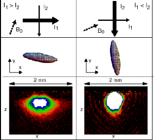
An example of a different configuration was realized in Munich with rubidium atoms. In this experiment, three-dimensional trapping was achieved by crossing two straight wires and choosing an appropriate bias field direction, as discussed in section II.1.4 (Reichel et al., 2001) (Fig. 34). Here the additional wire actually provides the endcaps that were previously provided in the Z– and U–shaped traps by the same wire. This type of trap might be useful for the realization of arrays of nearby traps. In Tübingen and Sussex longitudinal confinement has been achieved by additional coils.
Finally, the splitting of a single trap into two has been demonstrated in Heidelberg, Munich and Sussex. Such a time dependent potential is presented in Fig. 35 and as explained in section II, may form the basis of an interferometer. It is also the first step in creating multi well traps or arrays of traps.
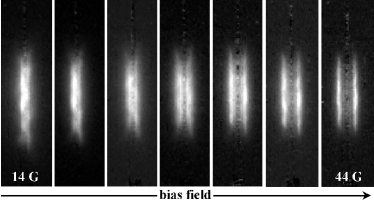
IV.3.2 Guiding and Transport
To achieve mesoscopic atom optics on a chip, it is essential to have reliable means of transporting atoms. One such device is an atomic guide using a single wire with a bias field. Such an experiment is shown in Fig. 36a. The Z–trap is transformed into an L–shaped guide by re-routing the current from one of the Z leads. The atoms expand along the guide due to their thermal velocity (Folman et al., 2000). Similarly, it was demonstrated that one can directly load the guide from a larger magnetic trap on the chip and skip the small surface trap.

It is also possible to achieve a continuously loaded magnetic guide using a leaky microtrap (see Fig. 36b). This is achieved by lowering the barrier between the trap and the guide, the barrier being simply the trap end cap, whose height may be controlled by changing the current in the microtrap (Brugger et al., 2000).
However, there are limitations to such a simple guide. Using a homogeneous external bias field, such a guide has to be straight (linear), since the bias field must be perpendicular to the wire as discussed in section II.1.2. This considerably limits the potential use of the whole chip surface. A possible solution is to create the bias field using on–chip wires (3-wire configuration shown in Fig. 2) or the two–wire guide configuration discussed in section II.1.3, in which the currents are counter propagating and the bias field is perpendicular to the chip surface. A first experiment was conducted by M. Prentiss’ group in Harvard (Dekker et al., 2000). Here, cesium atoms were dropped from a MOT onto a vertically positioned chip, on which a two–wire guide managed to deflect the atoms from their free fall (see Fig. 37). Furthermore, a four-wire guide was realized whereby the two extra wires served as the source for the bias field (see also Fig. 2). Guiding along a curved two wire guide has been achieved in Heidelberg, and experiments to guide atoms along a spiral are in progress (for the chip design see Fig. 29).
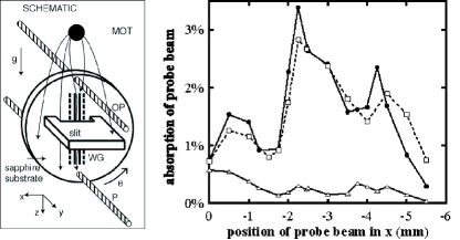
Several experiments have achieved guiding without any bias field by trapping the weak field seekers in the minimum existing exactly in between two parallel wires with co–propagating currents. This configuration was described in section II.1.3. In Fig. 38, we present such a setup (Müller et al., 1999). Another similar use of this principle (in this case, not surface mounted), in which a storage ring has been realized is presented in section III.1.7. Although advantageous for the lack of bias fields, this concept may be hard to implement on miniaturized atom chips as the atoms would be extremely close to the surface for m thick wires.
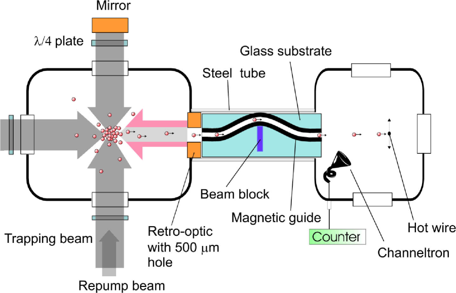
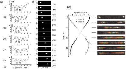
Guiding with semi–permanent magnets has also been achieved (Rooijakkers et al., 2001; Vengalattore et al., 2001). These materials enhance the magnetic fields coming from current carrying wires (see section II.1.10 for a description). Completely permanent magnets are also being contemplated to avoid current noise. However, to the best of our knowledge, only atom mirrors have thus far been realized this way (Hinds and Hughes, 1999).
A further limitation of the guides described above is that they rely on thermal velocity. Much more control can be achieved by transporting atoms using moving potentials, as described in section II.1.7. Such a transport device was implemented in an experiment in Munich. Using the movable 3-dimensional potentials of their ‘motor’, atoms can be extracted from a reservoir and moved or stopped at will (Hänsel et al., 2001a) (Fig. 39). This considerably improves the possibilities of the chip, as demonstrated by the ‘linear collider’ shown in Fig. 39c, in which the motor was used to split a cloud in two and then to collide the two halves (Reichel et al., 2001).
IV.3.3 Beam splitters
As discussed in section II.1.8, one may combine the wire guides as described in the previous section to build more complicated atom optical elements. One such element is a beam splitter. A simple configuration is a Y–shaped wire (Fig. 40a) which creates a beam splitter with one input guide for the atoms, the central wire of the Y, and two outputs guides, the right and left arms. The atoms are split by means of a symmetric scattering off the potential hill, which they encounter at the splitting point. Such a beam splitter on an atom chip was realized by Cassettari et al. (2000) in Innsbruck. Atoms were released from a chip microtrap and guided into the beam splitter. Depending on how the current in the input wire is sent through the Y, atoms can be switched from output arms of the Y to the other, or directed to the two outputs with any desired ratio (Fig. 40). Similar beam splitters have been widely used for the splitting of guided electron waves in solid–state quantum electronics devices. For example two Y splitters were put back to back to form an Aharonov-Bohm type interferometer (Buks et al., 1998).
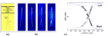
A four–port beam splitter has been realized at JILA by the group of E. Cornell and D. Anderson by making a near x-shape out of two wires which avoid a full crossing (Müller et al., 2000). In this experiment, two input guides formed by two current carrying wires, merge at the point of closest approach of the wires so that the two minima merge into one, and then again split into two independent minima.
IV.3.4 BEC on a chip
A degenerate quantum gas in a microtrap is an ideal reservoir from where to extract atoms for the experiments on the chip. For example a BEC will take a similar role as source of bosonic matter waves as the Fermi sea has in quantum electronics. A clear advantage of a BEC has to do with the transfer to the smallest compressed surface traps, which involves high compression, leading to large losses for thermal atoms if the trap depth is not appropriate. The condensate occupies the trap ground state and should follow any adiabatic compression of the trap. Second, a BEC in a microtrap also provides the initial atomic state needed to initiate delicate quantum processes such as interference or even a well defined entanglement between atoms in two nearby traps. The latter stands at the base of a two–qubit gate needed for quantum information processing.
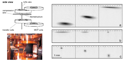
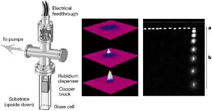
In the last year three groups in Tübingen, Munich and Heidelberg succeeded in making and holding a Bose–Einstein condensate in a surface trap (Ott et al., 2001; Hänsel et al., 2001), and the MIT group managed to transfer a BEC to a surface trap, and load it into it (Leanhardt et al., 2002). These experiments showed that making the BEC in a surface trap can be much simpler. For example in very tight micro traps the BEC is formed in much shorter time as the tightness of the traps allows for fast thermalization and consequently fast evaporative cooling which relaxes the vacuum requirements, permitting the use of a very simple one MOT setup to collect the atoms (Hänsel et al., 2001).
In the Tübingen experiment (Ott et al., 2001), a relatively large condensate of 87Rb atoms has been formed at a height of some m above the surface. The experiment made use of a pulsed dispenser as an atom source, allowing ultra high vacuum (mbar) while the dispenser was off. This enabled the use of a simple single MOT setup. The experiment was designed to transfer the atoms magnetically from a distant six beam MOT to the chip using two adjacent pairs of coils (Fig. 41). In the chip trap, condensation was reached after to s of forced RF evaporative cooling. Aside from being the first surface BEC, the chip used in Tübingen with its mm long wires provides a highly anisotropic BEC (aspect ratio ), approaching a quasi one–dimensional regime. In recent work, the BEC was taken to a height of only m without observing substantial heating (Fortagh et al., 2002). The smallest structure holding the BEC was a cross section copper wire with a current of A. The BEC had a lifetime of ms in the compressed trap (limited by 3–body collisions) and a s lifetime once it was expanded into a larger trap.
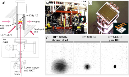
The second experiment producing a BEC in a microtrap was performed in Munich (Hänsel et al., 2001) (Fig. 42). Here an attractively simple setup with a continuous dispenser discharge was used. Consequently, the vacuum background pressure was high (mbar) and evaporative cooling had to be achieved quickly. RF cooling times were as short as ms thanks to the strong compression in the microtrap which results in a high rate of elastic collisions. The final BEC included some atoms at a height of m. The trapping wire was mm long and the trap aspect ratio was . The wire cross section was , and the current density approached . Strong heating of the cloud was observed in this experiment but the source remains elusive (possibly, current noise). A beautiful feature of this experiment is the use of the magnetic ‘conveyer belt’ described before (section II.1.7 and IV.3.2, Fig. 39), in order to transport the BEC during a time of ms over a distance of mm without destroying it (see Fig. 42). Furthermore, the ability of the ‘motor’ to split clouds was used to show that a BEC survives such a splitting. Two such halves were then released into free fall exhibiting interference fringes as they overlapped.
In the third experiment, performed in Heidelberg, the condensate of typically 87Rb atoms was formed either in a Z-wire joffe pritchard trap, created by a wire structure underneath the chip, or in a Z trap on the chip (Fig. 43). First atoms are loaded into a mirror MOT ( torr) created by external quadruople coils using a double MOT configuration with a continuous push beam. The atoms are then transferred into a U-MOT, where they are compressed and after molasses cooling loaded into a Z wire trap. The BEC is formed by forced RF evaporation in typically 20 seconds. Creating th BEC using a wire structure underneath the chip allows to place other surfaces close to the BEC, and still maintaining the high precision of a micro trap for manipulating the cold atoms. This will open up the possibility to either study surfaces with the cold atoms, and also to transfer the BEC to surface traps based on dipole forces in light fields created by micro-optic elements and evanescent fields.
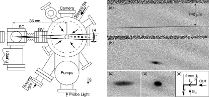
The MIT group has transported a BEC of the order of Na atoms into an auxiliary chamber and loaded it into a magnetic trap formed by a Z-shaped wire (Leanhardt et al., 2002)(Fig. 44). This was accomplished by trapping the condensate in the focus of an infrared laser and translating the location of the laser focus with controlled acceleration. This transport technique avoids the optical and mechanical access constraints, and the extreme UHV requirements of conventional condensate experiments. The BEC was consequently loaded into a micro structure.
Finally, we would like to note that currently other groups are also working towards BEC in surface traps, and in a short time we will see many different successful experiments
V Loss, heating and decoherence
For atom chips to work, three main destructive elements have to be put under control.
-
•
(i) Trap loss: It is crucial that we are able to keep the atoms inside the trap as long as needed.
-
•
(ii) Heating: Transfer of energy to our quantum system may result in excitations of motional degrees of freedom (e.g. trap vibrational levels), and consequently in multi mode propagation which would render the evolution of our system ill-defined.
-
•
(iii) Decoherence or dephasing as it is sometimes referred to also originates from coupling to the environment. While heating requires the transfer of energy, decoherence is more delicate in nature (Stern et al., 1990). Nevertheless, the effect is just as harmful because superpositions with a definite phase relation between different quantum states are destroyed. This has to be avoided, e.g. for interferometers or quantum information processing on the atom chip.
In discussing these three points, we focus on the particularities of atoms in strongly confined traps close to the surface of an atom chip. The small separation between the cold atom cloud and the ‘hot’ macroscopic environment raises the intriguing question of how strong the energy exchange will be, and which limit of atom confinement and height above the surface can ultimately be reached. We review theoretical results showing that fluctuations in the magnetic trapping potential give a fairly large contribution to both atom loss and heating. In addition, thermally excited near fields are also responsible for loss and may impose limits on coherent atom manipulation in very small (m sized) traps on the atom chip. Estimates for the relevant rates are given, and we outline strategies to reduce them as much as possible. Experimental data are not yet reliable enough to allow for a detailed test of the theory, but there are indications that field fluctuations indeed influence the lifetime of chip traps.
V.1 Loss mechanisms
V.1.1 Spilling over a finite potential barrier
Compression of a thermal atom cloud can lead to losses when the cloud temperature rises above the trap depth. The smallest losses occur if the compression is adiabatic. Atoms then stay in their respective energy levels as the level energy increases. They can nevertheless be lost during trap compression because of the finite trap depth. It should be noted that this loss occurs for the highest energies in the trap and can also be used to evaporatively cool the cloud (see Luiten et al. (1996) for a review).
V.1.2 Majorana flips
If the atomic magnetic moment is not able to follow the change in the direction of the magnetic field, the spin flips, and a weak field seeking atom can be turned into a strong field seeker which is not trapped (Majorana, 1932; Gov et al., 2000). This occurs when the adiabatic limit (Larmor frequency much larger than trap frequency ) does not hold. Majorana flips thus happen at or near zeros of the magnetic field. For this reason, additional bias fields are employed to ‘plug the hole’ in the center of a quadrupole field.
For a magnetic field configuration with a zero, loss can be reduced if the atoms circle around it. The loss rate is then inversely proportional to the angular momentum because the latter determines the overlap with the minimum region (Bergeman et al., 1989; Hinds and Eberlein, 2000).
In Ioffe-Pritchard traps with nonzero field minimum , there is a finite residual loss rate that has been calculated by Sukumar and Brink (1997). For a model atom with spin 1/2 in the vibrational ground state, one gets
| (18) | |||||
where is the component of the magnetic moment parallel to the trapping field. Note the exponential suppression for a sufficiently large plugging field , typical of nonadiabatic (Landau-Zener) transitions. Choosing a Larmor frequency , one gets a lifetime larger than trap oscillation periods. A ratio pushes this limit already to .
V.1.3 Noise-induced flips
Fluctuations in the magnetic trap fields can also induce spin flips into untrapped states, and lead to losses. These fluctuations are produced by thermally excited currents in the metallic substrate or simply by technical noise in the wire currents. Fluctuations of electric fields and of the Van der Waals atom-surface interaction have been shown to be less relevant for typical atom traps (Henkel and Wilkens, 1999; Henkel et al., 1999).
The trapped spin is perturbed via the magnetic dipole interaction and flips at a rate given by second-order perturbation theory:
| (19) |
where is the noise spectrum of the magnetic fields, taken at the Larmor frequency . We use the following convention for the noise spectrum
| (20) |
where is a time average (experiment) or an ensemble average (theory). The rms noise is thus given by an integral over positive frequencies
| (21) |
For example, the rms magnetic field in a given bandwidth for a white noise spectrum is given by . The spectrum thus has units .
| Geometry | Tr |
|---|---|
| Half-space | |
| Layer | |
| Wire |
Thermally excited currents
An explicit calculation of the magnetic noise due to substrate currents (‘near field noise’) yields the following estimate for the loss rate (Henkel et al., 1999)
| (22) |
where is the substrate conductivity (for copper, ) and the substrate temperature. Note that the Larmor frequency actually does not enter the loss rate. The ‘geometric tensor’ has dimension (1/length) and is inversely proportional to the height of the trap center above the surface (table 2). The loss rate (22) is quite large for a trap microns above a bulk metal surface. One can reduce the loss by two orders of magnitude when bulk metal in the vicinity of the trap is replaced by microstructures. For a thin metallic layer of thickness , the loss rate (22) is proportional to , and for a thin wire (diameter ), a faster decrease takes over (table 2).
The estimates of table 2 apply only in an intermediate distance regime, : on the one hand, when the trap distance is smaller than the size of the metallic structures, one recovers a behaviour characteristic for a metallic half-space; on the other hand, steeper power laws take over at large distances, when gets comparable to or larger than the skin depth
| (23) | |||||
Recall that the skin depth characterizes the penetration of high-frequency radiation into a metal. This crossover can be seen in Fig. 45 where the flip rate (22) is plotted vs. the trap height for a metallic half-space. For details, we refer to Henkel et al. (1999) and Henkel and Pötting (2001). Note that an increase of the Larmor frequency only helps to reduce the substrate-induced flips in the regime where . Eq.(23) shows that this requires, for , quite large Larmor frequencies GHz, meaning large magnetic (bias) fields.
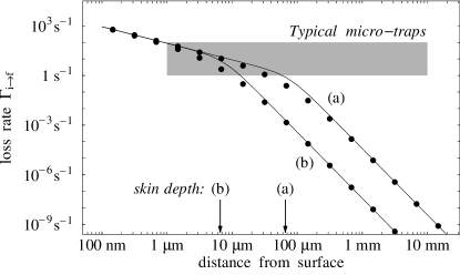
Technical noise
Additional loss processes may be related to fluctuations in the currents used in the experiment, for example in the chip wires and in the coils producing the bias and compensation fields. Let us focus on the wire current and denote its noise spectrum. Neglecting the finite wire size, the magnetic field is given by (3), and we find the following upper limit for the noise-induced flip rate
| (24) | |||||
where the reference value corresponds to shot noise at a wire current of 1A (). This estimate is pessimistic and assumes equal noise in both field components parallel and perpendicular to the static trapping field. Nevertheless, it highlights the need to use ‘quiet’ current drivers for atom chip traps. In future chip traps with strong confinement, it may turn out necessary to reduce current noise below the shot noise level. This can be achieved with permanent magnets, as discussed in section II.1.10 and reviewed by Hinds and Hughes (1999). Superconducting wires might provide an alternative solution, but we are unaware of investigations in this area, an exception being the relatively old paper by Varpula and Poutanen (1984).
V.1.4 Collisional losses
Background collisions
Here, collisions between background gas atoms and trapped atoms endow the latter with sufficient energy to escape the trap. In order to estimate the loss rate per atom , let us assume that the background gas is dominated by hydrogen molecules and at room temperature. We then get:
| (25) | |||||
where is the background pressure. Typical collision cross sections are in the range (Bali et al., 1999). As a general rule, one gets a trap lifetime of a few seconds in a vacuum of mbar. It is clear that vacuum requirements will become more stringent as longer interaction times are required.
Collisions of trapped atoms
For traps in UHV conditions, and especially for highly compressed traps and high density trapped samples, the dominant collisional loss mechanisms involve collisions between trapped atoms. The scattering of two atoms leads to a loss rate per atom scaling with the density, while 3-body collision rates scale with the density squared.
Spin exchange This process corresponds to inelastic two-body collisions where the hyperfine spin projections are conserved, but not the spins themselves. In the alkali atoms 7Li, 23Na, and 87Rb, for example, a collision between two weak field seeking states can lead to the emergence of two strong field seekers that are not trapped. This transition requires an excess energy of the order of the hyperfine splitting to occur, which is typically not available in cold atom collisions. Exothermic collisions between the weak field seekers , , and are not suppressed, however. The corresponding rate constant is proportional to where () are the scattering lengths in the singlet (triplet) diatomic potential (Côté et al., 1994). For 87Rb, these scattering lengths are accidentally very close, leading to a very small spin flip rate (Moerdijk and Verhaar, 1996; Burke et al., 1997). As a consequence, 87Rb is practically immune to spin exchange and can form stable condensates, even of two hyperfine species (Myatt et al., 1997; Julienne et al., 1997; Kokkelmans et al., 1997). Spin polarized samples consisting only of cannot undergo spin exchange because of conservation, the other available states having smaller . For more details, we refer to the review by Weiner et al. (1999) and references therein.
Spin relaxation This process also results from inelastic two-body collisions, but does not conserve . Spin relaxation is caused by a flip of the nuclear spin and occurs at a lower rate because of the smaller nuclear magnetic moment. In 87Rb for example, the trapped weak field seeker may be changed into the untrapped strong field seeker . More details can be found in the theoretical work by Burke et al. (1997); Julienne et al. (1997); Timmermans and Côté (1998), the experimental work of Gerton et al. (1999) and Söding et al. (1998) and the review paper by Weiner et al. (1999).
Three-body recombination In this process, two atoms combine to form a molecule. Although the molecules may have a definite magnetic moment and be still trapped, the reaction releases the molecular binding energy that is shared as excess kinetic energy between the molecule and the third atom. The binding energy being typically quite large (larger than 100eV), both partners escape the trap (Fedichev et al., 1996; Moerdijk and Verhaar, 1996; Moerdijk et al., 1996; Esry et al., 1999). For references to experimental work, see Burt et al. (1997); Söding et al. (1999) and Weiner et al. (1999). We expect three-body processes to be the dominant collisional decay channel in strongly compressed traps because the collision rate per atom increases with the square of the atomic density.
V.1.5 Tunneling
Traps very close to the surface might also show loss due to tunneling of atoms out of the local minimum of the trap towards the surface. The rate can be estimated from
| (26) |
where is the height of the barrier above the energy of the trapped particle. Tunneling will therefore only be important for states close to the top of the potential barrier. Low lying states in traps where the magnetic field magnitude rises for long distances will have very little tunneling. Even for atom waveguide potentials as close as 1m from the surface, tunneling lifetimes of more than 1000s have been estimated (Schmiedmayer, 1998; Pfau and Mlynek, 1996).
V.1.6 Stray light scattering
Residual light can flip the atomic spin via optical pumping. For resonant light, this happens at a rate of the order of where is the linewidth of the first strong electric dipole transition (typically, MHz) and the saturation intensity (typically a few mW/cm2). It is highly desirable to perform atom chip experiments ‘in the dark’: a shielding from any stray light at the level is required for manipulations on a scale of seconds. For more detailed estimates, we refer to the review by Grimm et al. (2000) on optical traps. An overview of the previous loss mechanisms is given in table 3.
| Mechanism | Scaling | Magnitude | Workaround |
|---|---|---|---|
| Spilling over | deep trap | ||
| Background collisions111111Eq.(25). | vacuum | ||
| Majorana flips121212Flip rate (18) from trap ground state | avoid B=0 | ||
| Near field | little metal | ||
| noise131313Eq.(22). The exponent for metal half-space, layer, and wire (see table 2). The estimate is for a half-space. | |||
| Current noise141414Eq.(24). | quiet drivers | ||
| 2-body spin exchange151515Experimental result for 87Rb (Myatt et al., 1997) | spin polarize | ||
| 2-body spin relaxation161616Experimental result for Cs and 7Li, respectively (Söding et al., 1998; Gerton et al., 1999) | |||
| 3-body collisions171717Experimental result for 87Rb and 7Li, respectively (Burt et al., 1997; Söding et al., 1999; Gerton et al., 1999) | |||
| Tunneling | thick barrier | ||
| Stray light | keep in dark |
We expect that on the route towards m sized traps with high compression, inelastic collisions and magnetic field noise will dominate the trap loss.
V.2 Heating
In the previous section, regarding loss mechanisms, heating was mentioned in relation to adiabatic compression where some atoms gain energies larger than the trap depth. Here, we discuss a different form of heating in which the atom exchanges energy with the environment. Such heating does not necessarily cause the atom to be lost, but it is still very harmful as excitations of vibrational degrees of freedom lead to an ill defined quantum state of the system. In the case of the atom system and the chip environment, the environment is always hot compared to the system. Energy exchange thus increases both the system’s mean energy and its energy spread. In the following, we first describe the influence of position and frequency noise using the harmonic oscillator model, then turn to substrate and technical noise, and finally touch upon the issue of heating due to light fields.
V.2.1 Harmonic oscillator model
Let us consider the trap potential to be a one dimensional harmonic potential with angular frequency and with a ground state size of , where is the mass of the vibrating atom. Assume for simplicity that the atom is initially prepared in the oscillator ground state . Heating can occur as a result of a fluctuating trap either in frequency or position (see for example Gehm et al. (1998); Turchette et al. (2000)). These processes may be described by transition rates to higher excited states of the oscillator. For example, fluctuations in the trap position (amplitude noise) are equivalent to a force acting on the atom. They drive the transition between the ground and first excited vibrational states, with an excitation rate given by (Gehm et al., 1998; Henkel et al., 1999)
| (27) |
that is determined by the noise spectrum of the force at the oscillator frequency . The rate of energy transfer to the atom (‘heating rate’) is simply or . Note that this estimate remains valid for an arbitrary initial state.
We may make contact with the work of Gehm et al. (1998) by noting that fluctuations of the trap center are equivalent to a force
| (28) |
In terms of the fluctuation spectrum of the trap center , the excitation rate (27) is thus given by
| (29) |
which is equivalent to the heating rate (12) of Gehm et al. (1998), given our definition (20) of the noise spectrum.
Fluctuations of the trap frequency are described by the Hamiltonian and heat the atom by exciting the transition. The corresponding transition rate is (Gehm et al., 1998)
| (30) |
and involves the frequency noise spectrum at twice the trap frequency. Using the rates given by Gehm et al. (1998), one can show that the heating rate due to frequency fluctuations is equal to , where the mean energy in the ground state.
In the following, we differentiate between thermal fluctuations and technical ones. To get the total heating rate, one simply adds the force fluctuation spectra of all the relevant sources (e.g. electromagnetic noise from radio stations).
V.2.2 Thermal fluctuations
Magnetic fields generated by thermally excited currents in the metallic substrate correspond to a force given by the gradient of the Zeeman interaction . An explicit calculation of the magnetic gradient noise gives the following force spectrum (Henkel and Wilkens, 1999; Henkel et al., 1999)
| (31) |
where is the magnetic moment and its component parallel to the static trapping field. The expression (31) applies to a planar metallic substrate (half-space) and an oscillation perpendicular to its surface. Again, the noise spectrum is actually frequency independent as long as where is the skin depth 23. The average magnetic moment is taken in the trapped spin state (see Henkel et al. (1999) for details). We thus obtain the following estimate for the excitation rate (27):
| (32) |
For lithium atoms, a typical trap frequency of kHz and a height of m, we estimate a heating rate of . For time scales typical of atom chip experiments (1–100ms), thermal fluctuations thus lead to tolerable heating only for traps with nm.

V.2.3 Technical noise
Heating due to technical noise may arise due to fluctuations in the currents which are used in the experiment. Noise in the chip wire currents and in the bias and compensation fields, for example, randomly shifts the location of the trap center. Let us focus on fluctuations in the chip wire current . Neglecting finite size effects, the current and the bias field produce the magnetic trap at a height of (eq. 3). The conversion from the current noise spectrum to the force spectrum required for the heating rate (27) is simply
| (33) |
and we end up with an excitation rate
| (34) |
The reference for the current noise is again the shot noise level at A. Note that this rate increases with the trap frequency: while a strong confinement suppresses heating from thermal fields (eq. 32), the inverse is true for trap position fluctuations. This is because in a potential with a large spring constant, position fluctuations translate into large forces (eq. 28). Typical trap parameters (kHz, G) lead for 7Li atoms to an excitation rate of . This estimate shows that even for very quiet currents technical noise is probably the dominant source of heating on the atom chip.
The fluctuations of the trap center (location proportional to ) can be reduced by correlating the currents of the bias field coils and the chip wire so that they have the same fluctuations, up to shot noise. Heating due to fluctuations in the trap frequency may then be relevant, as is proportional to (eq. 6). Let us again calculate an example. For a fixed ratio (due to correlated currents), we find for the relative frequency fluctuations
| (35) |
and hence an excitation rate (30)
| (36) |
Typical atom chip parameters (kHz, ) lead to which is negligible when compared to the rate obtained in (34).
V.2.4 Light heating
Another source of heating are the external light fields with which the atoms are manipulated and detected. Here the Lamb Dicke parameter is a convenient tool, where
| (37) |
is the ratio between the ground state size of the trap and the wave length of the impinging wave. This becomes clear if we remember that the probability not to be excited is simply the well known Debye-Waller factor
| (38) |
where is the momentum loss of the impinging photon. Hence, if the atoms are confined below the photon wave length (the so-called Lamb-Dicke limit ), they will not be heated by light scattering. Loss via optically induced spin flips is still relevant, however, as discussed in section V.1.6 and reviewed by Grimm et al. (2000).
In table 4 we give an overview of the heating mechanisms discussed above. For microscopic traps, we expect noise from current fluctuations and (to a lesser extent) from the thermal substrate to be the dominant origins of heating. Note the scaling with the trap frequency: trap fluctuations due to technical noise become more important for guides with strong confinement.
In this subsection, we have restricted ourselves to heating due to single-atom effects. Collisions with background gas atoms also lead to heating and rate estimates have been given by Bali et al. (1999). Finally, in a Bose condensate on chip, fluctuating forces may be expected to drive collective and quasiparticle excitations, leading to a depletion of the condensate ground state (Henkel and Gardiner, 2002). This area deserves further study in the near future.
| Noise | Scaling | Rate | Workaround |
|---|---|---|---|
| Near field181818Eq.(32), for a metal half-space. | |||
| Current191919Eq.(34). Note the scalings and for trap frequency and height. | correlate | ||
| currents | |||
| Trap frequency202020Eq.(36). | |||
| Light scattering | reduce | ||
| stray light |
V.3 Decoherence
We now turn to the destruction of quantum superpositions or interferences due to the coupling of the atom cloud to the noisy chip environment. This is an important issue when coherent manipulations like interferometry or qubit processing are to succeed on the atom chip. With chip traps being ever closer to the chip substrate, thermal and technical magnetic noise is expected to contribute seriously to decoherence, as it does to loss and heating processes.
The theoretical framework for describing decoherence makes use of the density matrix for the trapped atoms. Its diagonal elements give the occupation probabilities, or populations, in some preferred basis, usually the stationary trap states. Their evolution has been discussed in the previous subsections in terms of simple rate equations. Decoherence deals with the decay of off-diagonal elements, or coherences, of the density matrix. Their magnitude can be related to the fringe contrast one obtains in an interference experiment. Magnetic fluctuations typically affect both populations and coherences: field components perpendicular to the trapping fields redistribute the populations and parallel components suppress the coherences. The latter case illustrates that decoherence can occur even without the exchange of energy, because it suffices that some fluctuations randomize the relative phase in quantum superposition states (Stern et al., 1990). Such fluctuations are sometimes called ‘phase noise’.
In this subsection we consider first the decoherence of internal atomic states and then describe the impact of fluctuations on the center-of-mass. In the same way as for the heating mechanisms, we leave aside the influence of collisions on decoherence, nor do we consider decoherence in Bose-Einstein condensates.
V.3.1 Internal states
The spin states of the trapped atom are promising candidates for the implementation of qubits. Their coherence is reduced by transitions between spin states, induced by collisions or noise. The corresponding rates are the same as for the loss processes discussed in subsec. V.1.
In addition, pure phase noise occurs in the form of fluctuations in the longitudinal magnetic fields (along the direction of the trapping field). These shift the Larmor frequency in a random fashion and hence the relative phase between spin states. The corresponding off-diagonal density matrix element (or fringe contrast) is proportional to where is the phase shift accumulated during the interaction time . A ‘decoherence rate’ can be defined by
| (39) |
where is the spectrum of the frequency fluctuations. Two spin states , for example, ‘see’ a frequency shift , that involves the differential magnetic moment and the component of the magnetic field noise parallel to the trap field. The spectrum is then proportional to the spectrum of the magnetic field fluctuations.
Eq. (39) is derived in a rotating frame where the phase shift has zero mean and making the assumption that the spectral density is essentially constant in the frequency range . The noise then has a correlation time much shorter than the interaction time . We consider, as usual in theory, that is a random variable with Gaussian statistics, and get a fringe contrast
| (40) |
that decays exponentially at the rate (39).
Let us give an estimate for the decoherence rate due to magnetic noise. If are the magnetic fluctuations at the trap center, the shift of the Larmor frequency is given by
| (41) |
Here, the average magnetic moment is taken in the spin state trapped in the static trap field, thus picking the component parallel to the trap field. The noise spectrum of this field component, for thermal near field noise, is of the same order of magnitude as for the perpendicular component (Henkel et al., 1999) and depends only weakly on frequency. We thus get a decoherence rate comparable to the loss rate (22), typically a few . The same argument can be put forward for fluctuations in the wire current and the bias field. Assuming a flat current noise spectrum at low frequencies, we recover the estimate (24) for spin flip loss (a few ). Therefore, keeping the atoms in the trap, and maintaining the coherence of the spin states requires the same effort.
We finally note that near field magnetic noise also perturbs the coherence between different hyperfine states that have been suggested as qubit carriers. Although these states may have the same magnetic moment (up to a tiny correction due to the nuclear spin), excluding pure phase noise, their coherence is destroyed by transitions between hyperfine states. The corresponding loss rate (relevant, e.g., for optical traps) has been computed by Henkel et al. (1999) and is usually smaller than the spin flip rate.
V.3.2 Motional decoherence
The decoherence of the center-of-mass motion of a quantum particle has been put forward as an explanation for the classical appearance of macroscopic objects since the work of Zeh (1970) and Zurek (1991) (see also the book by Giulini et al. (1996)). It has be shown that the density matrix of a free particle subject to a random force field evolves into a diagonal matrix in the position basis (Zurek, 1991)
| (42) |
Here, the distance denotes how off-diagonal the element is, and is the momentum diffusion coefficient. The ‘coherence length’ thus decreases like
| (43) |
At the same time, the momentum spread increases, so that the relation is maintained at all times. For a particle trapped in a potential, the density matrix tends to a diagonal matrix in the potential eigenstate basis if the timescale for decoherence is large compared to the oscillation time . Typically, this applies be for the oscillatory motion in atom chip waveguides. The opposite case of ‘fast decoherence’ is discussed by Zurek et al. (1993) and Paz et al. (1993) and leads to the ‘environment-induced selection’ of minimum uncertainty (or coherent) states.
In the following we discuss different decoherence mechanisms for a typical separated path atom interferometer on the atom chip.
V.3.3 Longitudinal decoherence
We focus first on the quasi-free motion along the waveguide axis (the -axis), using the free particle model mentioned above. Decoherence arises again from magnetic field fluctuations due to thermal or technical noise. The corresponding random potential is given by (41):
| (44) |
where we retain explicitly the position dependence. Henkel and Pötting (2001) have shown that for white noise, the density matrix in the position representation behaves as
| (45) |
where the decoherence rate depends on the spatial separation between the two parts of the atomic wave function being observed:
| (46) |
Here, is the normalized spatial correlation function of the potential (equal to unity for ), and the noise spectrum characterizes the strength of the magnetic noise at the waveguide center.
For an atom chip waveguide perturbed by magnetic near field noise, the decoherence rate is of the order of
| (47) |
and hence comparable to the spin flip rate (19, 22). Decoherence should thus typically occur on a timescale of seconds. The correlation function is well approximated by a Lorentzian, as shown by Henkel et al. (2000), and the decoherence rate (46) can be written
| (48) |
where is the correlation length of the magnetic noise. This length can be taken equal to the height of the waveguide above the substrate (Henkel et al., 2000). This is because each volume element in the metallic substrate generates a magnetic noise field whose distance-dependence is that of a quasi-static field (a power law). Points at the same height above the surface therefore see the same field if their distance is comparable to . At distances , the magnetic noise originates from currents in uncorrelated substrate volume elements, and therefore . The corresponding saturation of the decoherence rate (48), , has also been noted, for example, by Cheng and Raymer (1999).
Decoherence due to magnetic noise from technical sources will also happen at a rate comparable to the corresponding spin flip rate, as estimated in (24). The noise correlation length may be comparable to the trap height because the relevant distances are below the photon wavelength at typical electromagnetic noise frequencies, so that the fields produced by wire current fluctuations are quasi-static, and the same argument applies. The noise correlation length of sources like the external magnetic coils will, of course, be much larger because these are far away from the waveguide. These rough estimates for the spatial noise properties of currents merit further investigation, in particular at the shot noise level.
Spatial decoherence as a function of time is illustrated in Fig. 47 where the density matrix averaged over is plotted. Note that this quantity will be directly proportional to the visibility of interference fringes when two wavepackets with a path difference are made to overlap and interfere. One sees that for large splittings , the coherence decays rapidly on the timescale given in (47). This is because the parts of the split wavepacket are subject to essentially uncorrelated noise. In a typical waveguide at height m, fringe contrast is thus lost after about a second (the spin lifetime) for path differences m. Increasing the height to m decreases by at least one order of magnitude as shown by (22). In addition, the correlation length grows to m, and larger splittings remain coherent. Alternatively, one can choose smaller splittings which decohere more slowly because the interferometer arms see essentially the same noise potential. Note, however, that the spin lifetime will always be the upper limit to the coherence time of the cloud.
The previous theory allows to recover the decoherence model of eq. (42) at long times . In this limit, only separations have not yet decohered, and we can make the expansion
| (49) |
for the decoherence rate (48). From the density matrix (45), we can then read off the momentum diffusion constant .

V.3.4 Transverse decoherence
We finally discuss the decoherence of a spatially split wavepacket in an atom chip interferometer, as described in section II.1.9. The excitation of transverse motional states in each arm suppresses this decoherence at the same rate as the heating processes discussed in subsec. V.2 (about ). Note that due to the transverse confinement, the relevant noise frequencies are shifted to higher values compared to the longitudinal decoherence discussed before.
The coherence between the spatially separated interferometer arms is suppressed in the same way as the longitudinal coherence discussed in section V.3.3. To show this, we use an argument based on phase noise and focus again on magnetic field fluctuations, either of thermal or technical origin. Magnetic fluctuations affect both the bottom of the trap well and the transverse trap frequency, but are only relevant when they differ in the spatially separated arms. The well bottoms get differentially shifted from an inhomogeneous bias field, e.g., while the trap frequency shifts due to changes in the field curvature.
We generalize the formula (39) to a phase shift that is the accumulation of energy level differences along the paths in the two arms. The decoherence (or dephasing) rate is thus given by
| (50) |
where is the spectral density of the energy difference, extrapolated to zero frequency.
To make contact with the density matrix formulation of eq. (45), we write where are the energy shifts in the right and left interferometer arms that are ‘seen’ by an atom travelling through the waveguide. We find
| (51) |
where the last two terms contain the correlation between the noise in both arms. They may therefore be expressed through the normalized correlation function with the separation between the left and right arms. The reasonable assumption that both arms ‘see’ the same white noise spectrum, say , yields
| (52) | |||||
| (53) |
where we recover the decoherence rate (46) obtained for the quasi-free longitudinal motion. We also recover the trivial result that the contrast stays constant if both interferometer arms are subject to the same noise amplitude (perfect correlation ).
The previous argument shows that transverse and longitudinal coherence are affected in a similar way by magnetic noise. Again, near field noise is a serious threat due to its short correlation length. Since the decoherence rate is so small that for interaction times not longer than a few hundred ms, the phase noise remains small even for widely separated arms subject to decorrelated noise (separation larger than the guide height). This is a worst-case estimate: a more careful approach would take into account the form of the interferometer, where the arm separation is not constant. Current noise should neither be underestimated. It is certainly possible to reduce dephasing by feeding the same current through both left and right wire guides, as shown by (53). But this does not seem to help at the shot noise level because each electron randomly follows one or the other wire. The wire current fluctuations are thus uncorrelated, leading to a transverse decoherence rate comparable to the longitudinal decoherence rate. Both rates are thus of the order of the flip rate (24), typically a few .
Let us estimate as another example the dephasing due to technical noise in a magnetic field gradient. This may be introduced by an imperfect Helmholtz configuration or coil misalignment. For small gradients , we have
| (54) |
where is the spatial separation between the interferometer arms. To be precise, gives the gradient of the bias field component along the direction of the (static) trapping field. Ignoring a possible anisotropy in the gradient noise, we find the estimate
| (55) |
where is related to the power spectrum of the current difference in the Helmholtz coils. We may take as the worst case completely uncorrelated Helmholtz currents, and a magnetic gradient where is the size of the Helmholtz coils. The dephasing rate is then of the order of
| (56) |
where are the Helmholtz current and the bias field. The experimentally reasonable parameters yield the small value . We note that the residual gradient of imperfect Helmholtz coils is usually less than G/cm which is an order of magnitude below the estimate G/cm taken here.
Finally, let us estimate the phase noise due to fluctuations in the spring constant of the guide potential. Even in the adiabatic limit where the transitions between transverse quantum states are suppressed (no heating), these fluctuations shift the energy of the guided state. In the harmonic approximation, we have for the ground state of the guide where is the relative shift of the vibration frequency. This gives a dephasing rate
| (57) |
We have neglected noise correlations between the interferometer arms that would reduce decoherence because of correlated phase shifts in both arms. The rate (57) is of the same order as the heating rate (30, 36) due to frequency noise (). It thus appears that fluctuations of the trap frequency have a larger impact than bias field gradients, but still they lead to negligible dephasing.
In table 5 we give an overview of the different decoherence mechanisms discussed in this subsection. For interferometers with large path differences (compared to the waveguide height), we expect current shot noise and thermal near field fluctuations to be the dominant sources of decoherence. They appear quite ‘rough’ (small correlation length) and perturb both the quasi-free motion along the waveguide axis and the relative phase between spatially separated wavepackets in an interferometer. An increase in the trap frequency does not help, rather the amount of metallic material in the vicinity of the guide should be kept to a minimum.
| Noise mchanism | Scaling | Rate | Workaround |
|---|---|---|---|
| Substrate fields212121Exponent for metal half-space, layer, and wire (eq. 22 and table 2). | |||
| little metal, | |||
| small splitting | |||
| Current 222222Eq.(34). | correlate currents | ||
| Bias fluctuations232323Eq.(56). The bias field scales as where is the size of the bias coils. | |||
| Trap frequency 242424Eq.(36). | |||
VI Vision and outlook
Much has been achieved in the field of micro-optics with matter waves in the last 10 years. We have seen a steady development from free standing wires to micron size traps and guides, from trapping thermal atoms to the creation of BEC on an atom chip. Where to go from here? What can we expect from future integrated matter wave devices? There are still many open questions before we can assess the full promise of integrated microscopic atom optics.
In the following paragraphs we try to pinpoint the relevant future developments and directions. Some of them like the study of the influence of the warm thermal surface and the fundamental noise limits on lifetime, heating and coherence of atoms, are already under way. Hopefully in a few years we will know how far micro manipulation of atoms on chips can be pushed.
VI.1 Integrating the atom chip
VI.1.1 Chip fabrication technology
We will see continued development of atom chip fabrication techniques. Depending on how close to the surface one is able to place atoms before significant decoherence occurs, the commonly used technology will be either state of the art nano fabrication with scale limits below 100nm or thicker and larger wires built by a combination of less demanding techniques. Another limitation would be smoothness of fabrication: as fluctuations in wire widths would cause changing current densities and consequently changing trap frequencies, potential hills’ may appear which may be large enough to hinder the transport of a BEC or control its phase evolution (for the same reason bias field stability will have to be improved in the future).
In the near future many advances are expected. One of the first steps will be to build multi layer structures that will enable for example crossing wires in order to realize more elaborate potentials and give more freedom for atom manipulation.
Thin film magnetic materials should allow to build permanent magnetic microscopic devices, which can be switched on and off for loading and manipulation of atoms. Such structures would have the advantage that the magnetic fields are much more stable, and consequently one can expect much longer coherence times, when compared with current generated fields.
VI.1.2 Integration with other techniques
With cold atoms trapped close to a surface, integration with many other techniques of atom manipulation onto the atom chip is possible.
One of the first tasks will be to integrate present day atom chips with existing micro optics (see for example Birkl et al. (2001)) and solid state optics (photonics), for atom manipulation and detection. We envision for example micro fabricated wave guides and/or micro fabricated lenses on the atom chip for bringing to and collecting light from atoms in the atom optical circuits.
Light can also be used for trapping (Grimm et al., 2000). Having cold atoms close to a surface will allow efficient transfer and precise loading of atoms into light surface traps, which would be otherwise difficult because of their small volume and inaccessible location. For example an atom chip with integrated micro optics, will allow to load atoms into evanescent wave guides and traps, as proposed by Barnett et al. (2000). Such traps and guides would be a way to circumvent the decoherence caused by Johnson noise in a warm conducting surface (section V).
With the standing wave created by reflecting light off the chip surface one will be able to generate 2-dimensional traps with strong confinement in one direction, resembling quantum wells, as demonstrated by Gauck et al. (1998). Adding additional laser beams or additional electrodes on the surface restrict the atomic motion further, yielding 2-dimensional devices as in quantum electronics (Imry, 1987). Similarly one can build and load optical lattices close to the surface where each site can be individually addressed by placing electrodes on the chip next to each site.
In principle, many other quantum optical components can be integrated on the atom chip. For example high Q cavities combined with micro traps will allow atoms to be held inside the cavity to much better than the wavelength of light providing a strong coupling between light and atoms. For recent experimental work concerning the manipulation and detection of atoms in cavities, we refer the reader to Berman (1994); Pinkse et al. (2000); Hood et al. (2000); Osnaghi et al. (2001); Guthöhrlein et al. (2001).
Regarding cavities one can think of examining a wide variety of technologies ranging from standard high Q cavities consisting of macroscopic mirrors to optical fiber cavities (with Bragg reflectors or with mirrors on the ends); from photonic band gap structures to micro cavities like micro spheres and micro discs fabricated from a suitable transparent material. One proposed implementation is presented in Fig. 48 (Mabuchi et al., 2001).
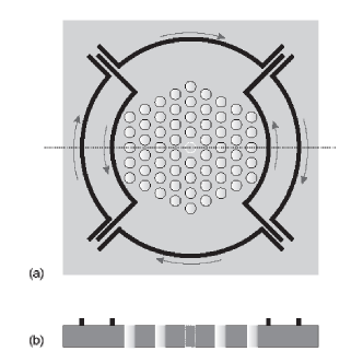
VI.1.3 Atom detection
For future applications, it would be advantageous to have a state selective single atom detector integrated on the atom chip. Such detectors could be based on different methods. The most direct method would be to detect the fluorescent light of the atom using surface mounted micro optics. More accurate non-destructive methods could be based on measuring an optical phase shift induced by an atom in a high Q cavity.
Single atom detection using near field radiation:
To detect light scattered from single atoms near a chip surface, the main challenge will be to minimize the stray light scattered from the surface. One possible solution may be to collect a large fraction of the light scattered by the atom using near field apertures and/or confocal microscope techniques. An atom could also be used to couple light between two wave guides, as used in some micro optic detectors for molecules and directional couplers in telecommunication.
Detecting single atoms by selective ionization:
This may be achieved using a multi step process up to a Rydberg state. The electron and the location from where it came can then be detected with a simple electron microscope. Using a dipole blockade mechanism as discussed by Lukin et al. (2001) one should be able to implement an amplification mechanism, which will allow 100% detection efficiency (Schmiedmayer et al., 2002)
Transmission of resonant light through a small cavity:
Such a scheme may be used to detect single atoms even for moderate Q values of the cavity. The cavity could be created by two fibers with high reflectivity coatings at the exit facets, or even by a DBR fiber cavity with a small gap for the cold atoms. Fiber ends molded in a lens shape could considerably reduce the light losses due to the gap. Having atoms localized in steep traps should allow a small gap that would reduce the losses even further.
Transmission of light through a high Q cavity:
Here, the transmission is modified by the presence of single atoms. In the high Q case, the light may be quite far from atomic resonance and the atoms are still detected with high probability. The basic mechanism of this detector is that atoms inside the cavity change the dispersion for the light. The high Q value makes it possible to detect very small modifications of the dispersion. In addition the cavities can be incorporated into integrated optics interferometers to measure the phase shift introduced by the presence of the atoms. Off resonant detection would allow for nondestructive atom detection (see for example Domokos et al. (2000)).
VI.2 Mesoscopic physics
The potentials created on an atom chip are very similar in scale and confinement to the potentials confining electrons in mesoscopic quantum electronics (Imry, 1987). There electrons move inside semiconductor structures, in our case atoms move above surfaces in atom optical circuits. In both cases they can be manipulated using potentials in which at least one dimension is comparable to the de Broglie wavelength of the guided, trapped particle. To find similarities and differences between mesoscopic quantum electronics and mesoscopic atom optics will probably become a very rich and fascinating research field.
Electrons in semiconductors interact strongly with the surrounding lattice. It is therefore hard to maintain their phase coherence over long times and distances. An atomic system on the contrary is well isolated. Furthermore, atoms (especially in a BEC) can be prepared such that the temperature is extremely low with respect to the energy level spacing. The consequence is that phase coherence is maintained over much longer times and distances. This might enable us to explore new domains in mesoscopic physics, which are hard to reach with electrons.
VI.2.1 Matter wave optics in versatile potentials
A degenerate quantum gas in the atom chip will allow us to study matter wave optics in confined systems with non trivial geometries, as splitters, loops, interferometers, etc. One can think of building rings, quantum dots connected by tunnel junctions or quantum point contacts (Thywissen et al., 1999b), or even nearly arbitrary combinations thereof in matter wave quantum networks. For many atomic situations the electronic counterparts can easily be identified. Atom chips will allow to probe a wide parameter range of transverse ground state widths, confinement and very large aspect ratios of and more. Atomic flow can be monitored by observing the expansion from an on-board reservoir along the conduit. Further perturbations and corrugations can be added at any stage to the potential by applying additional electric, magnetic or light fields to modify the quantum wire or quantum well. In this manner we can also explore how disorder in the guides may change the atomic behavior.
In the following, we give details regarding three exemplary matter wave potentials on the atom chip.
VI.2.2 Interferometers
In the near future it will be essential to develop and implement interferometers, and to study through them the decoherence of internal states and external motional states. Atom chip interferometers have been discussed in detail in section II.1.9. They can be built either in the spatial (Andersson et al., 2002) or the temporal domain (Hinds et al., 2001; Hänsel et al., 2001b). Integrated on an atom chip, they are very sensitive devices that may be used to measure inertial forces or even to perform computation (Andersson and Barnett, 2000). Coherence properties in more complicated networks can be studied by observing interference and speckle patterns.
Interferometers can also serve as probes for the understanding of surface–atom interactions allowing for a quantitative test of the limits imposed on the atom chip by the warm surface for both internal state and external (motional) state coherence. Since many of the important parameters scale with the spin flip life time in a trap (see section V), a first important step would be to measure the (BEC) lifetime in a micro trap as a function of distance to the surface. Aside from heating and spin flips, the surface also induces ‘phase noise’. Interferometers will be able to measure this subtle effect as a function of surface material type and temperature as well as atom-surface distance and spatial spread of the atomic superposition, through a reduction in the fringe visibility. Finally, by coupling micro traps (atomic quantum dots) to one of the interferometer arms, similar to the mesoscopic electron experiments (Buks et al., 1998), subtle interaction terms may be investigated, e.g., 1/r second order dipole interactions discussed by O’Dell et al. (2000).
Internal state superpositions of atoms close to surfaces can be studied using internal state interferometers. Using Raman transitions or microwave transitions we can create superpositions, observe their lifetime and put theoretical estimates to the test.
VI.2.3 Low dimensional systems
Much is known about the behavior of fermions in low dimensional strongly confining systems (one and two-dimensional systems) from mesoscopic quantum electronic experiments. By designing low dimensional experiments using atoms (weakly interacting bosons or fermions) we expect to obtain further insight also about electronic phenomena.
The role of interactions inside an atomic matter wave can range from minimal in a very dilute system to dominating in a very dense system. Low dimensional systems are especially interesting in this context, since it is expected that the interactions between the atoms will change for different potentials. The study of the dependence of the interactions (scattering length) on the dimensionality and the degree of confinement of the system (Olshanii, 1998; Görlitz et al., 2001; Petrov et al., 2000), will benefit due to the variety of potentials available on the atom chip.
VI.2.4 Non-linear phenomena
Another example of an interesting regime for the study of atom-atom interaction or non-linearity are multi-well potentials. Again, as mentioned in the context of interferometers, the splitting of a cloud of atoms into these multi sites can be either temporal or spatial. Here calculations beyond mean field theory are relevant, and new insight may be acquired. For example, one expects a crossover from coherent splitting to number splitting in different potential configurations, depending on the height of the potential barrier, the density, and the scattering length (Menotti et al., 2001; Vardi and Anglin, 2001; Orzel et al., 2001; Greiner et al., 2002).
VI.2.5 Boundary between macroscopic and microscopic description
Let us end this sub-section concerning mesoscopics by noting that the ability to change the number of atoms in a system, or alternatively to address specific atoms in an interacting ensemble, will allow us to probe the boundary between the macroscopic and microscopic description. Starting from a large system, we will try to gain more and more control over the system parameters, imprinting quantum behavior onto the system. On the other hand we can try and build larger and larger systems from single quantum objects (in modern lingo called qubits), and keep individual control over the parameters. Success in such an undertaking would bring us much closer to implementing quantum information transfer and quantum information processing as discussed below.
VI.3 Quantum information
The implementation of quantum information processing requires (DiVincenzo, 2000): (i) storage of the quantum information in a set of two-level systems (qubits), (ii) the processing of this information using quantum gates, and (iii) reading out the results. For a review of quantum computation we refer the reader to Bouwmeester et al. (2000).
We believe that quantum optical schemes where the qubit is encoded in neutral atoms can be implemented using atom optics on integrated atom chips (Schmiedmayer et al., 2002). These promise to combine the outstanding features of quantum optical proposals, in particular quantum control and long decoherence times, with the technological capabilities of engineering micro-structures implying scalability, a feature usually associated with solid state proposals. Let us review some of the requirements:
The Qubit
Using neutral atoms, the qubit can be encoded in two internal, long lived states (e.g. two different hyperfine electronic ground states). Single-qubit operations are induced as transitions between the hyperfine states of the atoms. These are introduced by external fields, using RF pulses like in NMR or in Ramsey-Bordé interferometers, Raman transitions or adiabatic passage.
One method to realize a qubit is to write the qubits into single atoms, which requires selective cooling and filling of atoms into the qubit sites. However, recently it was proposed that single qubits can also be written into an ensemble of atoms using ‘dipole blockade’ (Lukin et al., 2001). This may be simpler as it avoids the need for single atom loading of traps. As it will be pointed out, the dipole blockade mechanism can also be used to manipulate the qubit.
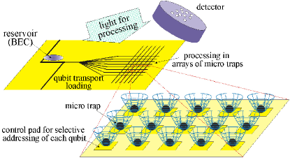
Entangling Qubits
The fundamental two-qubit quantum gate requires state selective interaction between two qubits, which is more delicate to implement. A two-qubit quantum gate is a state dependent operation such as a control not gate:
| (58) |
A good way to implement such a quantum gate is by state selective interactions, which can be switched on and off at will. This interaction can be between the qubits themselves, or mediated by a ‘bus’. Neutral atoms naturally interact with each other. To achieve different phase shifts for different qubit states, either the interaction between the qubits has to be state selective, or it has to be turned on conditioned on the qubit state. There are different ways to implement quantum gates in atom optics: depending on the interaction, we distinguish between (a) the generic interactions between the atoms, like the Van der Waals interaction (Jaksch et al., 1999; Calarco et al., 2000; Briegel et al., 2000), dipole-dipole interactions (Brennen et al., 1999; Brennen and Deutsch, 2000) and (b) interactions which can be switched on and off, for example dipole-dipole interactions (Jaksch et al., 2000; Lukin et al., 2001) between Rydberg states.
Dipole-blockade quantum gates between mesoscopic atom ensembles
Lukin et al. (2001) devised a technique for the coherent manipulation of quantum information stored in collective excitations of many-atom mesoscopic ensembles by optically exciting the ensemble into states with a strong atom-atom interaction. Under certain conditions the level shifts associated with these interactions can be used to block the transitions into states with more than a single excitation. The resulting dipole-blockade phenomenon closely resembles similar mesoscopic effects in nanoscale solid-state devices. It can take place in an ensemble with a size that can exceed many optical wavelengths and can be used to perform quantum gate operations between distant ensembles, each acting as a single qubit.
Cavity QED
The 2-qubit processing operation may be realized through a direct interaction (entanglement) between two atoms or through an intermediate ‘bus’. A light mode of a high Q cavity can serve as such a ‘bus’ acting on an array of atoms trapped inside the cavity (Pellizzari et al., 1995). Atoms in high Q cavities which in turn are connected with fibers, can also act as a converting device between ‘flying’ qubits (photons) which transverse distances, and storage qubits (atoms). The same principle can be used for entangling atoms in different cavities for a ‘distributed’ computation process (van Enk et al., 1998, 1999). In all of the above, the atom chip promises to enhance the feasibility of accurate atom-cavity systems.
Input/Output
Even without high Q cavities, an integrated atom chip, with atoms trapped in well controlled microtraps and with individual site light elements, can probably provide input/output processes by making use of techniques such as light scattering from trapped atomic ensembles (Duan et al., 2001), slow light (Hau et al., 1999; Vitali et al., 2000), stopped light (Phillips et al., 2001; Liu et al., 2001; Fleischhauer and Lukin, 2002) or macroscopic spin states (Duan et al., 2000; Julsgaard et al., 2001).
Let us summarize the road map for quantum computation with the atom chip: one would need to implement, (a) Versatile traps to accurately control atoms up to the stage of entanglement, (b) Controlled loading of single qubits (atoms or excitations) into these traps in well defined internal and external states, (c) Manipulation and detection of individual qubits, (d) Control over decoherence and (e) Scalability to be able to achieve controlled quantum manipulation of a large number of qubits.
VII Conclusion
Neutral-atom manipulation using integrated micro-devices is a new and extremely promising experimental approach. It promises to combine the best of two worlds: the ability to use cold atoms - a well controllable quantum system, and the immense technological capabilities of nanofabrication, micro optics and micro electronics to manipulate and detect the atoms.
In the future, a final integrated atom chip will have a reliable source of cold atoms with an efficient loading mechanism, single mode guides for coherent transportation of atoms, nano-scale traps, movable potentials allowing controlled collisions for the creation of entanglement between atoms, high resolution light fields for the manipulation of individual atoms, and internal state sensitive detection of atoms. All of these, including the bias fields and possibly even the light sources and the read-out electronics, could be on-board a self-contained chip. Such a robust and easy to use device, would make possible advances in many different fields of quantum physics: from applications such as clocks, sensors and implementations of quantum information processing and communication, to new experimental insight into fundamental questions relating to decoherence, dissorder, non-linearity, entanglement and atom scattering in low dimensional physics.
Acknowledgement
Foremost we would like to thank all the members of the Innsbruck, now Heidelberg, atom chip group for their enthusiasm and enormous effort they put into the experiments. We would like to personally thank our long time theoretical collaborators Peter Zoller, Tommaso Calarco and Robin Côté. The atom chips for the Innsbruck-Heidelberg experiments were fabricated by Thomas Maier at the Institut für Festkörperelektronik, Technische Universität Wien, Austria, and by Israel Bar-Joseph at the Sub-micron center, Weizmann Inst. of Science, Israel. We would also like to extend a warm thanks to the entire atom chip community for responding so positively to our requests for information and figures. Our work was supported by many sources, most notably the Austrian Science Foundation (FWF), project SFB S065-05, F15-07, the Deutsche Forschungsgemeinschaft Schwerpunktprogramme: Quanten Informationsverarbeitung and Wechselwirkungen in ultrakalten Atom- und Molekülgasen, the Institute for Quantum Information, and the European Union, contract numbers IST-1999-11055 (ACQUIRE), HPRI-CT-1999-00069 (LSF), TMRX-CT96-0002, and HPMF-CT-1999-00235.
References
- Dowling and Gea-Banacloche (1996) J. P. Dowling and J. Gea-Banacloche, Adv. At. Mol. Opt. Phys. 37, 1 (1996).
- Grimm et al. (2000) R. Grimm, M. Weidemüller, and Y. B. Ovchinnikov, Adv. At. Mol. Opt. Phys. 42, 95 (2000).
- Hinds and Hughes (1999) E. A. Hinds and I. G. Hughes, J. Phys. D 32, R119 (1999).
- Vladimirskii (1961) V. V. Vladimirskii, Sov. Phys. JETP 12, 740 (1961).
- Schmiedmayer (1992) J. Schmiedmayer, in XVIII International Conference on Quantum Electronics Technical Digest (Vienna, 1992), p. 13.
- Schmiedmayer (1995a) J. Schmiedmayer, Appl. Phys. B 60, 169 (1995a).
- Schmiedmayer (1995b) J. Schmiedmayer, Phys. Rev. A 52, R13 (1995b).
- Schmiedmayer and Scrinzi (1996a) J. Schmiedmayer and A. Scrinzi, Phys. Rev. A 54, R2525 (1996a).
- Schmiedmayer and Scrinzi (1996b) J. Schmiedmayer and A. Scrinzi, Quantum Semiclass. Opt. 8, 693 (1996b).
- Denschlag (1998) J. Denschlag (1998), phD thesis, University of Innsbruck.
- Denschlag et al. (1999a) J. Denschlag, D. Cassettari, and J. Schmiedmayer, Phys. Rev. Lett. 82, 2014 (1999a).
- Pron’kov and Stroganov (1977) G. P. Pron’kov and Y. G. Stroganov, Sov. Phys. JETP 45, 1075 (1977).
- Blümel and Dietrich (1989) R. Blümel and K. Dietrich, Phys. Lett. A 139, 236 (1989).
- Blümel and Dietrich (1991) R. Blümel and K. Dietrich, Phys. Rev. A 43, 22 (1991).
- Voronin (1991) A. I. Voronin, Phys. Rev. A 43, 29 (1991).
- Hau et al. (1995) L. Hau, J. Golovchenko, and M. Burns, Phys. Rev. Lett. 74, 3138 (1995).
- Burke et al. (1996) J. P. Burke, Jr., C. H. Greene, and B. D. Esry, Phys. Rev. A 54, 3225 (1996).
- Berg-Sørensen et al. (1996) K. Berg-Sørensen, M. Burns, J. Golovchenko, and L. Hau, Phys. Rev. A 53, 1653 (1996).
- Frisch and Segrè (1933) R. Frisch and E. Segrè, Z. f. Physik 75, 610 (1933).
- Gott et al. (1962) Y. V. Gott, M. S. Ioffe, and V. G. Tel’kovskii, Nucl. Fusion Supplement 3, 1045 (1962).
- Pritchard (1983) D. Pritchard, Phys. Rev. Lett. 51, 1336 (1983).
- Bagnato et al. (1987) V. S. Bagnato, G. P. Lafyatis, A. G. Martin, E. L. Raab, R. N. Ahmad-Bitar, and D. E. Pritchard, Phys. Rev. Lett. 58, 2194 (1987).
- Thywissen et al. (1999a) J. H. Thywissen, M. Olshanii, G. Zabow, M. Drndić, K. S. Johnson, R. M. Westervelt, and M. Prentiss, Eur. Phys. J. D 7, 361 (1999a).
- Müller et al. (1999) D. Müller, D. Z. Anderson, R. J. Grow, P. D. D. Schwindt, and E. A. Cornell, Phys. Rev. Lett. 83, 5194 (1999).
- Sauer et al. (2001) J. A. Sauer, M. D. Barret, and M. S. Chapman, Phys. Rev. Lett. 87, 270401 (2001).
- Zokay and Garraway (2000) O. Zokay and B. M. Garraway, Opt. Commun. 93, 93 (2000).
- Hinds et al. (2001) E. A. Hinds, C. J. Vale, and M. G. Boshier, Phys. Rev. Lett. 86, 1462 (2001).
- Richmond et al. (1998) J. A. Richmond, S. NicChormaic, B. P. Cantwell, and G. I. Opat, Acta Phys. Slov. 48, 481 (1998).
- Denschlag et al. (1999b) J. Denschlag, D. Cassettari, A. Chenet, S. Schneider, and J. Schmiedmayer, Appl. Phys. B 69, 291 (1999b).
- Fortagh et al. (1998) J. Fortagh, A. Grossmann, and C. Zimmermann, Phys. Rev. Lett. 81, 5310 (1998).
- Fortagh et al. (2000) J. Fortagh, H. Ott, A. Grossmann, and C. Zimmermann, Appl. Phys. B 70, 701 (2000).
- Ott et al. (2001) H. Ott, J. Fortagh, G. Schlotterbeck, A. Grossmann, and C. Zimmermann, Phys. Rev. Lett. 87, 230401 (2001).
- Cassettari et al. (1999) D. Cassettari, A. Chenet, J. Denschlag, R. Folman, B. Hessmo, A. Haase, P. Krüger, S. Schneider, and J. Schmiedmayer, in Laser Spectroscopy, XIV International Conference, edited by R. Blatt, J. Eschner, D. Leibfried, and F. Schmidt-Kaler (World Scientific, 1999).
- Reichel et al. (1999) J. Reichel, W. Hänsel, and T. W. Hänsch, Phys. Rev. Lett. 83, 3398 (1999).
- Haase et al. (2001) A. Haase, D. Cassettari, B. Hessmo, and J. Schmiedmayer, Phys. Rev. A 64, 043405 (2001).
- Reichel et al. (2001) J. Reichel, W. Hänsel, P. Hommelhoff, and T. W. Hänsch, Appl. Phys. B 72, 81 (2001).
- Weinstein and Libbrecht (1995) J. D. Weinstein and K. Libbrecht, Phys. Rev. A 52, 4004 (1995).
- Drndić et al. (1998) M. Drndić, K. S. Johnson, J. H. Thywissen, M. Prentiss, and R. M. Westervelt, Appl. Phys. Lett. 72, 2906 (1998).
- Hänsel et al. (2001a) W. Hänsel, J. Reichel, P. Hommelhoff, and T. W. Hänsch, Phys. Rev. Lett. 86, 608 (2001a).
- Buks et al. (1998) E. Buks, R. Schuster, M. Heiblum, D. Mahalu, and V. Umansky, Nature 391, 871 (1998).
- Cassettari et al. (2000) D. Cassettari, B. Hessmo, R. Folman, T. Maier, and J. Schmiedmayer, Phys. Rev. Lett. 84, 1124 (2000).
- Müller et al. (2000) D. Müller, E. A. Cornell, M. Prevedelli, P. D. D. Schwindt, A. Zozulya, and D. Z. Anderson, Opt. Lett. 25, 1382 (2000).
- Andersson et al. (1999) E. Andersson, M. T. Fontenelle, and S. Stenholm, Phys. Rev. A 59, 3841 (1999).
- Hänsel et al. (2001b) W. Hänsel, J. Reichel, P. Hommelhoff, and T. W. Hänsch, Phys. Rev. A 64, 063607 (2001b).
- Andersson et al. (2002) E. Andersson, T. Calarco, R. Folman, M. Andersson, B. Hessmo, and J. Schmiedmayer, Phys. Rev. Lett. 88, 100401 (2002).
- Sidorov et al. (1996) A. I. Sidorov, R. J. McLean, W. J. Rowlands, D. C. Lau, J. E. Murphy, M. Walkiewicz, G. I. Opat, and P. Hannaford, JEOS – Quantum and Semiclassical Optics 8, 713 (1996).
- Meschede et al. (1997) D. Meschede et al., Spie Proc. 2995, 191 (1997).
- Saba et al. (1999) C. V. Saba, P. A. Barton, M. G. Boshier, I. G. Hughes, P. Rosenbusch, B. E. Sauer, and E. A. Hinds, Phys. Rev. Lett. 82, 468 (1999).
- Davis (1999) T. J. Davis, J. Opt. B 1, 408 (1999).
- Opat et al. (1992) G. I. Opat, S. J. Wark, and A. Cimmino, Appl. Phys. B 54, 396 (1992).
- Vengalattore et al. (2001) M. Vengalattore, W. Rooijakkers, and M. Prentiss (2001), physics/0106028.
- Hau et al. (1992) L. Hau, M. Burns, and J. Golovchenko, Phys. Rev. A 45, 6468 (1992).
- Denschlag and Schmiedmayer (1997) J. Denschlag and J. Schmiedmayer, Europhys. Lett. 6, 405 (1997).
- Denschlag et al. (1998) J. Denschlag, G. Umshaus, and J. Schmiedmayer, Phys. Rev. Lett. 81, 737 (1998).
- Paul (1990) W. Paul, Rev. Mod. Phys. 62, 531 (1990).
- Landau and Lifshitz (1976) L. D. Landau and E. M. Lifshitz, Mechanics (Pergamon, Oxford, 1976).
- Shimizu and Morinaga (1992) F. Shimizu and M. Morinaga, Jpn. J. Appl. Phys. 31, L1721 (1992).
- Batelaan et al. (1994) H. Batelaan, R. Abfalterer, S. Wehinger, and J. Schmiedmayer, in EQEC V Technical Digest (Amsterdam, 1994), p. 13.
- Schmiedmayer (1998) J. Schmiedmayer, Eur. Phys. J. B 4, 57 (1998).
- Roach et al. (1995) T. M. Roach, H. Abele, M. G. Boshier, H. L. Grossman, K. P. Zetie, and E. A. Hinds, Phys. Rev. Lett. 75, 629 (1995).
- Sekatskii et al. (2001) S. K. Sekatskii, B. Riedo, and G. Dietler, Opt. Comm. 195, 197 (2001).
- Calarco et al. (2000) T. Calarco, E. A. Hinds, D. Jaksch, J. Schmiedmayer, J. I. Cirac, and P. Zoller, Phys. Rev. A 61, 022304 (2000).
- Key et al. (2000) M. Key, I. G. Hughes, W. Rooijakkers, B. E. Sauer, E. A. Hinds, D. J. Richardson, and P. G. Kazansky, Phys. Rev. Lett. 84, 1371 (2000).
- Vuletic et al. (1996) V. Vuletic, T. W. Hänsch, and C. Zimmermann, Europhys. Lett. 36, 349 (1996).
- Vuletic et al. (1998) V. Vuletic, T. Fischer, M. Praeger, T. W. Hänsch, and C. Zimmermann, Phys. Rev. Lett. 80, 1634 (1998).
- Cassettari et al. (1998) D. Cassettari, A. Chenet, J. Denschlag, S. Schneider, and J. Schmiedmayer, in EQEC 98 Technical Digest (Glasgow, 1998).
- Haase (2000) A. Haase (2000), diploma thesis, University of Innsbruck.
- Rowlands et al. (1995) W. J. Rowlands, D. C. Lau, G. I. Opat, A. I. Sidorov, R. J. McLean, and P. Hannaford, in Laser Spectroscopy, XII International Conference, edited by M. Inguscio, M. Allegrini, A. Sasso, and L. Capri (Island of Capri, Italy, 1995), p. 134.
- Rowlands et al. (1996a) W. J. Rowlands, D. C. Lau, G. I. Opat, A. I. Sidorov, R. J. McLean, and P. Hannaford, Optics Comm. 126, 55 (1996a).
- Rowlands et al. (1996b) W. J. Rowlands, D. C. Lau, G. I. Opat, A. I. Sidorov, R. J. McLean, and P. Hannaford, Aust. J. Phys. 49, 577 (1996b).
- Shimizu et al. (1992) F. Shimizu, K. Shimizu, and H. Takuma, Jpn. J. Appl. Phys 31, L436 (1992).
- Fujita et al. (2000) J. Fujita, S. Mitake, and F. Shimizu, Phys. Rev. Lett. 84, 4027 (2000).
- Nowak et al. (1998) S. Nowak, N. Stuhler, T. Pfau, and J. Mlynek, Phys. Rev. Lett. 81, 5792 (1998).
- Gustavson et al. (2001) T. L. Gustavson, A. P. Chikkatur, A. E. Leanhardt, A. Görlitz, S. Gupta, D. E. Pritchard, and W. Ketterle, Phys. Rev. Lett. 88, 020401 (2001).
- Müller et al. (2001) D. Müller, E. A. Cornell, M. Prevedelli, P. D. D. Schwindt, Y. Wang, and D. Z. Anderson, Phys. Rev. A 63, 041602(R) (2001).
- Dekker et al. (2000) N. H. Dekker, C. S. Lee, V. Lorent, J. H. Thywissen, S. P. Smith, M. Drndić, R. M. Westervelt, and M. Prentiss, Phys. Rev. Lett. 84, 1124 (2000).
- Folman et al. (2000) R. Folman, P. Krüger, D. Cassettari, B. Hessmo, T. Maier, and J. Schmiedmayer, Phys. Rev. Lett. 84, 4749 (2000).
- Lee et al. (1996) K. I. Lee, J. A. Kim, H. R. Noh, and W. Jhe, Opt. Lett. 21, 1177 (1996).
- Pfau et al. (1997) T. Pfau, H. Gauck, D. Schneble, M. Hartl, and J. Mlynek, in Quantum Electronics Conf. Vol. 17 (OSA, Washington D.C., 1997).
- Schneble et al. (1999) D. Schneble, H. Gauck, M. Hartl, T. Pfau, and J. Mlynek, in Proceedings of the International School of Physics “Enrico Fermi”(Varenna 1998): Bose-Einstein Condensation in Atomic Gases, edited by M. Inguscio, S. Stringari, and C. Wieman (IOS Press, Amsterdam, 1999), p. 469.
- Gauck et al. (1998) H. Gauck, M. Hartl, D. Schneble, H. Schnitzler, T. Pfau, and J. Mlynek, Phys. Rev. Lett. 81, 5298 (1998).
- Schneble et al. (2001) D. Schneble, M. Hasuo, T. Anker, T. Pfau, and J. Mlynek, in QELS 2001, Technical Digest, Postconference Edition (OSA, Washington, 2001).
- Ketterle (1999) W. Ketterle, Physics Today 30 (1999).
- Briegel et al. (2000) H.-J. Briegel, T. Calarco, D. Jaksch, J. I. Cirac, and P. Zoller, J. Mod. Optics 47, 415 (2000).
- Brugger et al. (2000) K. Brugger, T. Calarco, D. Cassettari, R. Folman, A. Haase, B. Hessmo, P. Krüger, T. Maier, and J. Schmiedmayer, J. Mod. Optics 47, 2789 (2000).
- Rooijakkers et al. (2001) W. Rooijakkers, M. Vengalatorre, and M. Prentiss, in ICOLS proceedings (OSA, Washington, 2001).
- Hänsel et al. (2001) W. Hänsel, P. Hommelhoff, T. W. Hänsch, and J. Reichel, Nature 413, 498 (2001).
- Leanhardt et al. (2002) A. E. Leanhardt, A. P. Chikkatur, D. Kielpinski, Y. Shin, T. L. Gustavson, W. Ketterle, and D. E. Pritchard (2002), cond-mat/0203214.
- Fortagh et al. (2002) J. Fortagh, H. Ott, S. Kraft, and C. Zimmermann (2002), cond-mat/0205310.
- Stern et al. (1990) A. Stern, Y. Aharonov, and Y. Imry, Phys. Rev. A 41, 3436 (1990).
- Luiten et al. (1996) O. J. Luiten, M. W. Reynolds, and J. T. M. Walraven, Phys. Rev. A 53, 381 (1996).
- Majorana (1932) E. Majorana, Nuovo Cimento 9, 43 (1932).
- Gov et al. (2000) S. Gov, S. Shtrikman, and H. Thomas, J. Appl. Phys. 87, 3989 (2000).
- Bergeman et al. (1989) T. H. Bergeman, P. McNicholl, J. Kycia, H. Metcalf, and N. Balazs, J. Opt. Soc. B 6, 2249 (1989).
- Hinds and Eberlein (2000) E. A. Hinds and C. Eberlein, Phys. Rev. A 61, 033614 (2000), erratum: ibid. 64, 039902 (2001).
- Sukumar and Brink (1997) C. V. Sukumar and D. M. Brink, Phys. Rev. A 56, 2451 (1997).
- Henkel and Wilkens (1999) C. Henkel and M. Wilkens, Europhys. Lett. 47, 414 (1999).
- Henkel et al. (1999) C. Henkel, S. Pötting, and M. Wilkens, Appl. Phys. B 69, 379 (1999).
- Henkel and Pötting (2001) C. Henkel and S. Pötting, Appl. Phys. B 72, 73 (2001).
- Henkel and Scheel (2002) C. Henkel and S. Scheel (2002), in preparation.
- Varpula and Poutanen (1984) T. Varpula and T. Poutanen, J. Appl. Phys. 55, 4015 (1984).
- Bali et al. (1999) S. Bali, K. M. O’Hara, M. E. Gehm, S. R. Granade, and J. E. Thomas, Phys. Rev. A pp. R29–32 (1999).
- Côté et al. (1994) R. Côté, A. Dalgarno, and M. J. Jamieson, Phys. Rev. A 50, 399 (1994).
- Moerdijk and Verhaar (1996) A. J. Moerdijk and B. J. Verhaar, Phys. Rev. A 53, R19 (1996).
- Burke et al. (1997) J. P. Burke, J. L. Bohn, B. D. Esry, and C. H. Greene, Phys. Rev. A 55, R2511 (1997).
- Myatt et al. (1997) C. J. Myatt, E. A. Burt, R. W. Ghrist, E. A. Cornell, and C. E. Wieman, Phys. Rev. Lett. 78, 586 (1997).
- Julienne et al. (1997) P. S. Julienne, F. H. Mies, E. Tiesinga, and C. J. Williams, Phys. Rev. Lett. 78, 1880 (1997).
- Kokkelmans et al. (1997) S. J. J. M. F. Kokkelmans, H. M. J. M. Boesten, and B. J. Verhaar, Phys. Rev. A 55, R1589 (1997).
- Weiner et al. (1999) J. Weiner, V. S. Bagnato, S. Zilio, and P. S. Julienne, Rev. Mod. Phys. 71, 1 (1999).
- Timmermans and Côté (1998) E. Timmermans and R. Côté, Phys. Rev. Lett. 80, 3419 (1998).
- Gerton et al. (1999) J. M. Gerton, C. A. Sackett, B. J. Frew, and R. G. Hulet, Phys. Rev. A 59, 1514 (1999).
- Söding et al. (1998) J. Söding, D. Guéry-Odelin, P. Desbiolles, G. Ferrari, and J. Dalibard, Phys. Rev. Lett. 80, 1869 (1998).
- Fedichev et al. (1996) P. O. Fedichev, M. W. Reynolds, and G. V. Shlyapnikov, Phys. Rev. Lett. 77, 2921 (1996).
- Moerdijk et al. (1996) A. J. Moerdijk, H. M. J. M. Boesten, and B. J. Verhaar, Phys. Rev. A 53, 916 (1996).
- Esry et al. (1999) B. D. Esry, C. H. Greene, and J. J. P. Burke, Phys. Rev. Lett. 83, 1751 (1999).
- Burt et al. (1997) E. A. Burt, R. W. Ghrist, C. J. Myatt, M. J. Holland, E. A. Cornell, and C. E. Wieman, Phys. Rev. Lett. 79, 337 (1997).
- Söding et al. (1999) J. Söding, D. Guéry-Odelin, P. Desbiolles, F. Chevy, H. Inamori, and J. Dalibard, Appl. Phys. B 69, 257 (1999).
- Pfau and Mlynek (1996) T. Pfau and J. Mlynek, in Ultracold Atoms and Bose-Einstein-Condensation (Proceedings of the European Quantum Electronics Conference, sept. 1996, Hamburg, Germany), edited by K. Burnett, Trends in Optics and Photonics Series (Optical Society of America, Washington D. C., 1996), vol. 7, p. 33.
- Gehm et al. (1998) M. E. Gehm, K. M. O’Hara, T. A. Savard, and J. E. Thomas, Phys. Rev. A 58, 3914 (1998).
- Turchette et al. (2000) Q. A. Turchette, C. J. Myatt, B. E. King, C. A. Sackett, D. Kielpinski, W. M. Itano, C. Monroe, and D. J. Wineland, Phys. Rev. A 62, 053807 (2000).
- Henkel and Gardiner (2002) C. Henkel and S. A. Gardiner (2002), in preparation.
- Zeh (1970) H. D. Zeh, Found. Phys. 1, 69 (1970).
- Zurek (1991) W. H. Zurek, Physics Today 44, 36 (1991).
- Giulini et al. (1996) D. Giulini, E. Joos, C. Kiefer, J. Kupsch, I.-O. Stamatescu, and H. D. Zeh, Decoherence and the appearance of a classical world in quantum theory (Springer, Berlin Heidelberg New York, 1996).
- Zurek et al. (1993) W. H. Zurek, S. Habib, and J. P. Paz, Phys. Rev. Lett. 70, 1187 (1993).
- Paz et al. (1993) J. P. Paz, S. Habib, and W. H. Zurek, Phys. Rev. D 47, 488 (1993).
- Henkel et al. (2000) C. Henkel, K. Joulain, R. Carminati, and J.-J. Greffet, Opt. Commun. 186, 57 (2000).
- Cheng and Raymer (1999) C.-C. Cheng and M. G. Raymer, Phys. Rev. Lett. 82, 4807 (1999).
- Birkl et al. (2001) G. Birkl, F. B. J. Buchkremer, R. Dumke, and W. Ertmer, Opt. Commun. 191, 67 (2001).
- Barnett et al. (2000) A. H. Barnett, S. P. Smith, M. Olshanii, K. S. Johnson, A. W. Adams, and M. Prentiss, Phys. Rev. A 61, 023608 (2000).
- Imry (1987) Y. Imry, Introduction to Mesoscopic Physics (Oxford University Press, Oxford, 1987).
- Berman (1994) P. Berman, ed., Cavity quantum electrodynamics, Adv. At. Mol. Opt. Phys. (Academic Press, New York, 1994).
- Pinkse et al. (2000) P. W. H. Pinkse, T. Fischer, P. Maunz, and G. Rempe, Nature 404, 365 (2000).
- Hood et al. (2000) C. J. Hood, T. W. Lynn, A. C. Doherty, A. S. Parkins, and H. J. Kimble, Science 287, 1447 (2000).
- Osnaghi et al. (2001) S. Osnaghi, P. Bertet, A. Auffeves, P. Maioli, M. Brune, J. M. Raimond, and S. Haroche, Phys. Rev. Lett. 87, 037902 (2001).
- Guthöhrlein et al. (2001) G. R. Guthöhrlein, M. Keller, K. Hayasaka, W. Lange, and H. Walther, Nature 414, 49 (2001).
- Mabuchi et al. (2001) H. Mabuchi, M. Armen, B. Lev, M. Loncar, J. Vuckovic, H. J. Kimble, J. Preskill, M. Roukes, A. Scherer, and S. J. van Enk, Quantum Information and Computation 1, 7 (2001).
- Lukin et al. (2001) M. D. Lukin, M. Fleischauer, R. Cote, L. M. Duan, D. Jaksch, J. I. Cirac, and P. Zoller, Phys. Rev. Lett. 87, 037901 (2001).
- Schmiedmayer et al. (2002) J. Schmiedmayer, R. Folman, and T. Carlarco, Journ. Mod. Opt. (2002), (in print).
- Domokos et al. (2000) P. Domokos, M. Gangl, and H. Ritsch, Optics Communications 185, 115 (2000).
- Thywissen et al. (1999b) J. H. Thywissen, R. M. Westervelt, and M. Prentiss, Phys. Rev. Lett. 83, 3762 (1999b).
- Andersson and Barnett (2000) E. Andersson and S. M. Barnett, Phys. Rev. A 62, 052311 (2000).
- O’Dell et al. (2000) D. O’Dell, S. Giovanazzi, G. Kurizki, and V. M. Akulin, Phys. Rev. Lett. 84, 5687 (2000).
- Olshanii (1998) M. Olshanii, Phys. Rev. Lett. 81, 938 (1998).
- Görlitz et al. (2001) A. Görlitz, J. M. Vogels, A. E. Leanhardt, C. Raman, T. L. Gustavson, J. R. Abo-Shaeer, A. P. Chikkatur, S. Gupta, S. Inouye, T. P. Rosenband, et al., Phys. Rev. Lett. 87, 130402 (2001).
- Petrov et al. (2000) D. S. Petrov, G. V. Shlyapnikov, and J. T. M. Walraven, Phys. Rev. Lett. 85, 3745 (2000).
- Menotti et al. (2001) C. Menotti, J. R. Anglin, J. I. Cirac, and P. Zoller, Phys. Rev. A 63, 023601 (2001).
- Vardi and Anglin (2001) A. Vardi and J. R. Anglin, Phys. Rev. Lett. 86, 568 (2001).
- Orzel et al. (2001) C. Orzel, A. K. Tuchman, M. L. Fenselau, M. Yasuda, and M. A. Kasevich, Science 291, 2386 (2001).
- Greiner et al. (2002) M. Greiner, O. Mandel, T. Esslinger, T. W. Hänsch, and I. Bloch, Nature 415, 39 (2002).
- DiVincenzo (2000) D. P. DiVincenzo, Fortschritte der Physik 48, 771 (2000).
- Bouwmeester et al. (2000) D. Bouwmeester, A. Ekert, and A. Zeilinger, eds., The Physics of Quantum Information (Springer-Verlag, Heidelberg Berlin New York, 2000).
- Jaksch et al. (1999) D. Jaksch, H.-J. Briegel, J. I. Cirac, C. W. Gardiner, and P. Zoller, Phys. Rev. Lett. 82, 1975 (1999).
- Brennen et al. (1999) G. K. Brennen, C. Caves, P. Jessen, and I. Deutsch, Phys. Rev. Lett. 82, 1060 (1999).
- Brennen and Deutsch (2000) G. K. Brennen and I. H. Deutsch, Phys. Rev. A 61, 062309 (2000).
- Jaksch et al. (2000) D. Jaksch, J. I. Cirac, P. Zoller, S. L. Rolston, R. Côté, and M. D. Lukin, Phys. Rev. Lett. 85, 2208 (2000).
- Pellizzari et al. (1995) T. Pellizzari, S. A. Gardiner, and P. Zoller, Phys. Rev. Lett. 75, 3788 (1995).
- van Enk et al. (1998) S. J. van Enk, J. I. Cirac, and P. Zoller, Science 279, 205 (1998).
- van Enk et al. (1999) S. J. van Enk, H. J. Kimble, J. I. Cirac, and P. Zoller, Phys. Rev. A 59, 2659 (1999).
- Duan et al. (2001) L.-M. Duan, M. Lukin, J. I. Cirac, and P. Zoller, Nature 414, 413 (2001).
- Hau et al. (1999) L. V. Hau, S. E. Harris, Z. Dutton, and C. H. Behroozi, Nature 397, 594 (1999).
- Vitali et al. (2000) D. Vitali, M. Fortunato, and P. Tombesi, Phys. Rev. Lett. 85, 445 (2000).
- Phillips et al. (2001) D. F. Phillips, A. Fleischhauer, A. Mair, R. L. Walsworth, and M. D. Lukin, Phys. Rev. Lett. 86, 783 (2001).
- Liu et al. (2001) C. Liu, Z. Dutton, C. H. Behroozi, and L. V. Hau, Nature 409, 490 (2001).
- Fleischhauer and Lukin (2002) M. Fleischhauer and M. D. Lukin, Phys. Rev. A 65, 022314 (2002).
- Duan et al. (2000) L.-M. Duan, J. I. Cirac, P. Zoller, and E. S. Polzik, Phys. Rev. Lett. 85, 5643 (2000).
- Julsgaard et al. (2001) B. Julsgaard, A. Kozhekin, and E. S. Polzik, Nature 413, 400 (2001).
- Wing (1984) W. Wing, Prog. Quant. Electr. 8, 181 (1984).
- Ketterle and Pritchard (1992) W. Ketterle and D. Pritchard, Appl. Phys. B 54, 403 (1992).
- Shapere and Wilczek (1989) A. Shapere and F. Wilczek, eds., Geometric Phases in Physics (World Scientific, 1989).
- Aharonov and Stern (1992) Y. Aharonov and A. Stern, Phys. Rev. Lett. 69, 3593 (1992).
- Stern (1992) A. Stern, Phys. Rev. Lett. 68, 1022 (1992).
- Littlejohn and Weigert (1993) R. G. Littlejohn and S. Weigert, Phys. Rev. A 48, 924 (1993).
- Sekatskii and Schmiedmayer (1996) S. K. Sekatskii and J. Schmiedmayer, Europhys. Lett. 69, 3593 (1996).
- Palm and Thylén (1992) T. Palm and L. Thylén, Appl. Phys. Lett. 60, 237 (1992).
- Palm and Thylén (1999) T. Palm and L. Thylén, Phys. Rev. Lett. 82, 2564 (1999).
- Spreeuw et al. (2000) R. J. C. Spreeuw, D. Voigt, B. T. Wolschrijn, and H. B. van Linden van den Heuvell, Phys. Rev. A 61, 053604 (2000).
- Pfau (2001) T. Pfau (2001), private communication.
- Cook and Hill (1982) R. J. Cook and R. K. Hill, Opt. Commun. 43, 258 (1982).
- Ekstrom et al. (1992) C. R. Ekstrom, D. W. Keith, and D. E. Pritchard, Appl. Phys. B 54, 369 (1992).