Efficient wave function matching approach for quantum transport calculations
Abstract
The Wave Function Matching (WFM) technique has recently been developed for the calculation of electronic transport in quantum two-probe systems. In terms of efficiency it is comparable with the widely used Green’s function approach. The WFM formalism presented so far requires the evaluation of all the propagating and evanescent bulk modes of the left and right electrodes in order to obtain the correct coupling between device and electrode regions. In this paper we will describe a modified WFM approach that allows for the exclusion of the vast majority of the evanescent modes in all parts of the calculation. This approach makes it feasible to apply iterative techniques to efficiently determine the few required bulk modes, which allows for a significant reduction of the computational expense of the WFM method. We illustrate the efficiency of the method on a carbon nanotube field-effect-transistor (FET) device displaying band-to-band tunneling and modeled within the semi-empirical Extended Hückel theory (EHT) framework.
pacs:
73.40.-c, 73.63.-b, 72.10.-d, 85.35.Kt, 85.65.+hI Introduction
Quantum transport simulations have become an important theoretical tool for investigating the electrical properties of nano-scale systems. Datta (2005); Brandbyge et al. (2002); Büttiker et al. (1985); Meir and Wingreen (1992); Reed et al. (1997) The basis for the approach is the Landauer-Büttiker picture of coherent transport, where the electrical properties of a nano-scale constriction is described by the transmission coefficients of a number of one-electron modes propagating coherently through the constriction. The approach has been used successfully to describe the electrical properties of a wide range of nano-scale systems, including atomic wires, molecules and interfaces. Faleev et al. (2005); Pomorski et al. (2004); Gokturk (2005); Stilling et al. (2006); Nitzan and Ratner (2003); Di Ventra et al. (2000); Stokbro et al. (2003); Lang and Avouris (2000); Larade et al. (2001); Khomyakov and Brocks (2004) In order to apply the method to semiconductor device simulation, it is necessary to handle systems comprising many thousand atoms, and this will require new efficient algorithms for calculating the transmission coefficient.
Our main purpose in this paper is to give details of a method we have developed, based on the WFM technique, Ando (1991); Khomyakov et al. (2005); Brocks et al. (2007) which is suitable for studying electronic transport in large-scale atomic two-probe systems, such as large carbon nanotubes or nano-wire configurations.

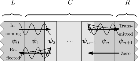
We adopt the many-channel formulation of Landauer and Büttiker to describe electron transport in nano-scale two-probe systems composed of a left and a right electrode attached to a central device, see Fig. 1. In this formulation, the conduction of incident electrons through the device is intuitively given in terms of transmission and reflection matrices, and , that satisfy the unitarity condition in the case of elastic scattering. The matrix element is the probability amplitude of an incident electron in a mode in the left electrode being scattered into a mode in the right electrode, and correspondingly is the probability of it being reflected back into mode in the left electrode. This simple interpretation yields the Landauer-Büttiker formula Büttiker et al. (1985)
| (1) |
which holds in the limit of infinitesimal voltage bias and zero temperature.
To our knowledge, the WFM schemes presented so far in the literature require the evaluation of all the Bloch and evanescent bulk modes of the left and right electrodes in order to obtain the correct coupling between device and electrode regions. The reason for this is that the complete set of bulk modes is needed to be able to represent the proper reflected and transmitted wave functions. In this paper we will describe a modified WFM approach that allows for the exclusion of the vast majority of the evanescent modes in all parts of the calculation. The primary modification can be pictured as a simple extension of the central region with a few principal electrode layers. In this manner, it becomes advantageous to apply iterative techniques for obtaining the relatively few Bloch modes and slowly decaying evanescent modes that are required. We have recently developed such an iterative method in Ref. Sørensen et al., 2008, which allows for an order of magnitude reduction of the computational expense of the WFM method in practice.
In this work, the proper analysis of the modified WFM approach is presented. The accuracy of the method is investigated and appropriate error estimates are developed. As an illustration of the applicability of our WFM scheme we consider a 1440 atom CNTFET device of 14 nm in length. We calculate the zero-bias transmission curves of the device under various gate voltages and reproduce previously established characteristics of band-to-band tunneling.Appenzeller et al. (2004) We compare directly the results of the modified WFM method to those of the standard WFM method for quantitative verification of the calculations.
The rest of the paper is organized as follows. The WFM formalism used to obtain and is introduced in Sect. II. In Sect. III we present our method to effectively exclude the rapidly decaying evanescent modes from the two-probe transport calculations. Numerical results are presented in Sect. IV. and the paper ends with a short summary and outlook.
II Formalism
In this section we give a minimal review of the formalism and notation that is used in the current work in order to determine the transmission and reflection matrices and . This WFM technique has several attractive features compared to the widely used and mathematically equivalent Green’s function approach. Datta (2005); Brandbyge et al. (2002) Most importantly, the transparent Landauer picture of electrons scattering via the central region between Bloch modes of the electrodes is retained throughout the calculation. Moreover, WFM allows one to consider the significance of each available mode individually in order to achieve more efficient numerical procedures to obtain and .
II.1 Wave function matching
The WFM method is based upon direct matching of the bulk modes in the left and right electrode to the scattering wave function of the central region. For the most part this involves two major tasks; obtaining the bulk electrode modes and solving a system of linear equations. The bulk electrode modes can be characterized as either propagating or evanescent (exponentially decaying) modes but only the propagating modes contribute to in Eq. (1). We may write , where
| (2) |
is the total transmission and the sum is limited to propagating modes and in the left and right electrode, respectively. Notice, however, that the evanescent modes are still needed in order to obtain the correct matrix elements . We will discuss this matter in Sect. III.3.
We assume a tight-binding setup for the two-probe systems in which the infinite structure is divided into principal layers numbered and composed of a finite central () region containing the device and two semi-infinite left () and right () electrode regions, see Fig. 2. The wave function is in layer , where denotes localized non-orthogonal atomic orbitals and are the positions of the orbitals in layer . We represent by a column vector of the expansion coefficients, given by , and write the wave function extending over the entire system as . We also assume that the border layers and of the central region are always identical to a layer of the connecting electrodes.
We refer the reader to Refs. Ando, 1991; Khomyakov et al., 2005; Brocks et al., 2007; Sørensen, 2008 for details on how to employ WFM to our setup. Here and in the rest of this paper, we will use the following notation for the key elements: The matrices contain in their columns the full set of left-going () and right-going () bulk modes of the left electrode, and the diagonal matrices hold the corresponding Bloch factors. 111 Bloch’s theoremAshcroft and Mermin (1976) for the ideal electrodes defines the phase factors , where is the complex wave number and is the layer thickness, which are referred to as Bloch factors throughout this paper. If trivial modes with or occur they are simply rejected. We assume that all the evanescent bulk modes are (state-)normalized , while all the Bloch bulk modes are flux-normalized 222 When using the Landauer formula in Eq. (1) it is assumed that the electrode Bloch modes carry unit current in the conduction direction. This can be conveniently accommodated by flux-normalizing the Bloch modes, i.e., , in the case of the left electrode.Fisher and Lee (1981) , where are the group velocitiesAshcroft and Mermin (1976); Khomyakov and Brocks (2004) and is the layer thickness. Similarly for the right electrode the matrices and are formed.
We also introduce the Bloch matricesKhomyakov et al. (2005) and . which propagate the layer wave functions in the bulk electrode
| (3) |
where subscript is implied for the left electrode (), and for the right electrode (). Notice that the first central region layer is defined for layer and not layer , as is the case in Ref. Brocks et al., 2007.
As explicitly shown in Refs. Ando, 1991; Khomyakov et al., 2005; Brocks et al., 2007, by fixing the layer wave functions coming into the region (e.g., in our case and ) and matching the layer wave functions across the region boundaries, the system of linear equations for the central region wavefunction can be written as
| (4) |
where is the energy, the overlap and the Hamiltonian matrix of the central region. In the following we discuss the terms, , , and , which arise from matching the boundary conditions with the electrode modes.
The self-energy matrices, and , arise from matching with the outgoing left and right electrode modes. They only have non-zero terms in the upper left and lower right corner block, respectively, and these elements can be calculated in terms of the Bloch matrices:Ando (1991); Khomyakov et al. (2005)
| (5) |
and
| (6) |
where we have introduced the overline notation and . For the current setup, these matrices are identical to the self-energy matrices introduced in the Green’s function formalism Datta (2005) (to within an infinitesimal imaginary shift of ), and may be evaluated by well-known recursive techniquesGuinea et al. (1983); Lopez Sancho et al. (1985) or constructed directly from the electrode modes using Eq. (6).
The source term arises from the incoming mode. Assuming an incoming mode from the left, we have specified by the expression
| (7) |
where is the incoming wave function.
For notational simplicity in the following sections, we leave out the implied subscripts or , indicating the left or right electrode, whenever the formalism is the same for both (e.g, for symbols , etc.).
II.2 Transmission and reflection coefficients
As a final step we want to determine the and matrices from the boundary wave functions and that have been obtained by solving Eq. (4).
When the incoming wave is specified to be the th right-going mode of the left electrode, then will be the superposition of outgoing right transmitted waves. The th column of the transmission matrix is defined as the corresponding expansion coefficients in right electrode modes and can be evaluated by solving
| (8) |
where is the column matrix holding the right-going bulk modes of the right electrode (and here assumed to be non-singular). Similarly the th column of the reflection matrix is given by
| (9) |
where holds the left-going bulk modes of the left electrode. The flux normalization ensures that .
III Excluding evanescent modes
| System | Atoms | Eq. (4) | Eq. (4)() | dgeev | This work |
|---|---|---|---|---|---|
| Fe–MgO–Fe | 27(6) | 0.8 | 0.9 | 1.3 | 1.1 |
| Al–C7–Al | 74(18) | 0.4 | 0.6 | 3.6 | 1.6 |
| Au–DTB–Au | 102(27) | 8.1 | 13.5 | 91.0 | 28.2 |
| Au–CNT(8,0)1–Au | 140(27) | 11.4 | 16.6 | 77.6 | 17.1 |
| Au–CNT(8,0)5–Au | 268(27) | 45.3 | 50.3 | 83.6 | 17.8 |
| CNT(8,0)–CNT(8,0) | 192(64) | 7.0 | 11.9 | 129.0 | 19.4 |
| CNT(4,4)–CNT(8,0) | 256(6464) | 7.2 | 12.4 | 121.5 | 21.0 |
| CNT(5,0)–CNT(10,0) | 300(4080) | 24.7 | 31.5 | 113.3 | 22.6 |
| CNT(18,0)–CNT(18,0) | 576(144) | 172.2 | 225.5 | 1362.2 | 253.3 |
| CNTFET (see Fig. 6) | 1440(160) | 259.8 | 286.9 | 4633.0 | 372.3 |
The most time consuming task of the WFM method is often to determine the electrode modes, which requires solving a quadratic eigenvalue problem.Ando (1991) As examples, see the profiling results listed in Table 1, where we have used the method to compute and for a selection of two-probe systems. 333 We should point out that the metallic electrodes in the two-probe systems considered in Table 1 can be fully described by much smaller unit cells than indicated (often only a few atoms are needed) and therefore the time spend on computing the bulk modes can be vastly reduced in these specific cases. For a general method, however, which supports CNTs, nano wires, etc. as electrodes, the timings are appropriate for showing the overall trend in the computational costs. The CPU timings show that to determine the electrode modes by employing the state-of-the-art lapack eigensolver dgeev is, in general, much more expensive than to solve the system of linear equations in Eq. (4). We expect this trend to hold for larger systems as well. Therefore, in the attempt to model significantly larger devices (thousands of atoms), it is of essential interest to reduce the numerical cost of the electrode modes calculation. We argue that a computationally reasonable approach is to limit the number of electrode modes taken into account, e.g., by excluding the least important evanescent modes. In this section, a proper technique to do this in a rigorous and systematic fashion is presented.
III.1 Decay of evanescent modes
The procedure to determine the Bloch factors and non-trivial modes of an ideal electrode and subsequently characterize these as right-going () or left-going () is well described in the literature.Ando (1991); Krstić et al. (2002); Khomyakov et al. (2005); Brocks et al. (2007) We note that only the obtained propagating modes with are able to carry charge deeply into the electrodes and thus enter the Landauer expression in Eq. (2). The evanescent modes with , on the other hand, decay exponentially but can still contribute to the current in a two-probe system, as the “tails” may reach across the central region boundaries.
Consider a typical example of an electrode modes evaluation: We look at a gold electrode with 27 atoms in the unit cell represented by 9 () orbitals for each Au-atom. Such a system results in 243 right-going and 243 left-going modes. Fig. 3a shows the positions in the complex plane of the Bloch factors corresponding to the right-going modes (i.e., ) for energy . We see that there are exactly three propagating modes, which have Bloch factors located on the unit circle. The remaining modes are evanescent, of which many have Bloch factors with small magnitude very close to the origin.
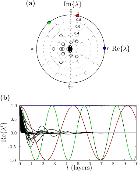
Fig. 3b illustrates how the 243 left-going modes would propagate through 10 successive gold electrode unit cells. The figure shows that the amplitudes of the three propagating modes are unchanged, while the evanescent modes are decaying exponentially. In particular, we note that the evanescent modes with Bloch factors of small magnitude are very rapidly decaying and vanishes in comparison to the propagating modes after only a few layers. In the following, we will exploit this observation and attempt to exclude such evanescent modes from the WFM calculation altogether. Formally this can be accomplished if only the electrode modes with Bloch factors satisfying
| (10) |
are computed and subsequently taken into account, for a reasonable choice of . Eq. (10) is adopted as the key relation to select a particular subset of the available electrode modes (as recently suggested in Ref. Khomyakov et al., 2005).
III.2 Extra electrode layers
We will denote the mode, Bloch and self-energy matrices from which the rapidly decaying evanescent modes are excluded with a tilde, i.e., as , and . The mode matrices holding the excluded modes are denoted by a math-ring accent , so that
| (11) |
is the assumed splitting of the full set. All expressions to evaluate the Bloch and self-energy matrices are unchanged as given in Sect. II (now merely represents the pseudo-inverses of ). However, since the column spaces of are not complete, there is no longer any guaranty that WFM can be performed so that the resulting self-energy matrices and, in turn, the solution of the linear system in Eq. (4), are correct. In addition, it is clear that errors can occur in the calculation of and from Eqs. (8) and (9) because the boundary wave functions and might not be fully represented in the reduced sets and .
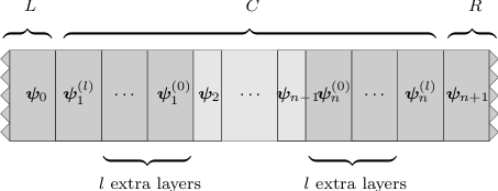
In order to diminish the errors introduced by excluding evanescent modes, we propose to insert additional electrode layers in the central region, see Fig. 4. As illustrated in the previous section, this would quickly reduce the imprint of the rapidly decaying evanescent modes in the boundary layer wave functions and , which means that the critical components outside the column spaces becomes negligible at an exponential rate in terms of the number of additional layers. We emphasize that the inserted layers may be “fictitious” in the sense that they can be accommodated by simple block-Gaussian-eliminations prior to the solving of Eq. (4) for the original system.
The above statements are confirmed by the following analysis. We expand the electrode wave functions in the corresponding complete set of bulk modes
| (12) |
where are vectors that contain the expansion coefficients. In the particular case, where extra electrode layers are inserted and the border layers of the region are identical to the connecting electrode layers, the electrode wavefunctions entering the matching boundary equations will be
| (13) |
and
| (14) |
using the definition . This shows that the critical components outside the column spaces of and are given by coefficients and , respectively. If this set only consists of the most rapidly decaying of the evanescent modes according to Eq. (10), that is, for the diagonal elements of and for the diagonal elements of , where is less than , these coefficients always decrease as a function of .
We conclude that WFM with the reduced set of modes approaches the exact case if additional electrode layers are inserted and the solution obtained from Eq. (4) approaches the correct solution accordingly.
III.3 Accuracy
As pointed out above, the exclusion of some of the evanescent modes from the mode matrices will introduce errors because the column spaces in are incomplete. In this section we will estimate how this will influence the accuracy of the calculated transmission and reflection coefficients in terms of the parameter and the number of extra electrode layers.
Consider first the accuracy of the transmission matrix in the case of the extended two-probe system in Fig. 4. For a specific incoming mode , we compare the correct result obtained with the complete set of modes (cf. Eq. (8)),
| (15) |
with the result obtained with the reduced mode matrix (denoted by a prime),
| (16) |
where represents the zero vector of size and the zero matrix of size .
The important coefficients in and for transmission calculations are the ones representing the Bloch modes which enters the Landauer-Büttiker formula in Eq. (2). Since these are never excluded they will always be located within the first elements, i.e., in and . It then suffices to compare these parts of the transmission matrix which we can do as follows.
From the properties of the pseudo-inverse we are able to write the relation
| (17) |
where is the identity matrix of order equal to the number of included modes . Using the expression in Eq. (14) it then follows that
| (18) |
and
| (19) |
where the expression clearly corresponds to the correct coefficients plus an error term.
We have already established in the previous section that the factor in the error term will decrease as a function of . We now show that the other term, is independent of , and consequently, that the error term in Eq. (19) must decrease as a function of . To this end we look at the 2-norm of , which satisfies
| (20) |
since when all evanescent modes are assumed to be normalized. The norm can be readily evaluated and depends on the set of modes included via the parameter but not on . Thus, we conclude that the only term of Eq. (19) which depend on is , and the error is therefore decreasing as function of .
Writing Eq. (19) as , where holds the errors on the coefficients of the th column, we further obtain that the total transmission can be expressed as
| (21) |
where is the exact result and the summation is over the Bloch modes and in the left and right electrode, respectively.
For a first order estimate of the error term in Eq. (21) we consider the worst case approximation, where all diagonal elements of are equal to the maximum range of Eq. (10). This makes all elements proportional to . and we arrive at the simple relation
| (22) |
which shows that the error decreases exponentially in terms of the number of extra layers .
For a higher order estimate of the error, we directly monitor the error arising on the boundary conditions, in terms of the coefficient vectors and , where and are given by solving Eq. (4). When the boundary conditions are exactly satisfied, we have and . In the case where the boundary conditions are not exactly satisfied, represents the error on the left-going components within the right boundary layer in the same way that represents the error on the right-going (transmitted) components. We would therefore expect the same order of magnitude of and in an actual calculation for a given mode . This suggests the following error estimate from Eq. (21),
| (23) |
where all the vector norms (e.g., ) are assumed to be taken over the elements corresponding to Bloch bulk modes only.
III.4 Example
To end this section, we exemplify the previous discussion quantitatively by looking at the Au(111) electrode described earlier, and assuming a 128 atom (4 unit cells) device of zigzag-(8,0) carbon nano tube (CNT) sandwiched between the gold electrodes, see the configuration in Fig. 1. For energy , we have calculated the deviation between the total transmission obtained when all bulk modes are taken into account () and when some evanescent modes are excluded () as specified with different settings of . Deviations are also determined for the corresponding total reflection coefficients ( and ). Fig. 5 shows the results as a function of , together with the estimate of Eq. (22) and the estimate of Eq. (23) both for the transmission and reflection coefficients, where the higher order terms have been neglected,
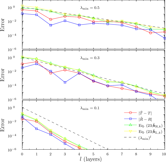
We observe that the absolute error in the obtained transmission coefficients (red curves) and reflection coefficients (blue curves) are generally decreasing as a function of , following the same convergence rate as (dashed line). Looking closer at results for neighbor values, we see that the errors initially exhibit wave-like oscillations. This is directly related to the wave form of the evanescent modes that have been excluded (see the propagation of the slowest decaying black curves in Fig. 3(b)). In other words, although the norm of the errors are decreasing as a function of , the specific error on a given (large) coefficient of or may increase, which means that the overall error term in Eq. (21) can go up. Fortunately this is only a local phenomenon with the global trend being rapidly decreasing errors.
Consider also the quality of the simple accuracy estimate of and the estimates expressed by Eq. (23) for the transmission coefficients (green curves) and reflection coefficients (yellow curves), respectively. For relatively large all estimates are very good. However, for smaller values of , only the latter two retain a high quality while the estimate tends to be overly pessimistic. It is important to remember that these estimates are by no means strict conditions but in practice give very reasonable estimates of the accuracy.
We note in passing, that the results in the top panel of Fig. 5 corresponds to using only the propagating Bloch modes in the transmission calculation. Still we are able to compute and to an absolute accuracy of three digits by inserting extra electrode layers in the two-probe system. This is quite remarkable and shows promise for large-scale systems, e.g., with nano-wire electrodes, for which the total number of evanescent modes available becomes exceedingly great.
IV Application
In this section we will apply the developed method to a nano-device consisting of a CNT stretched between to two metal electrodes and controlled by three gates. The setup is inspired by Appenzeller et al.,Appenzeller et al. (2004) and we expect this particular arrangement to be able to display so-called band-to-band (BTB) tunneling, where one observes gate induced tunneling from the valence band into the conduction band of a semi-conducting CNT and vice versa.
We show the configuration of the two-probe system in Fig. 6. The device configuration contains 10 principal layers of a CNT(8,4), having 112 atoms in each layer. The diameter of the tube and the thickness of the principal layer are 8.3 Å and 11.3 Å, respectively. The electrodes consist of CNT(8,4) resting on a thin surfaces of Li, where the lattice constant of the Li layers is stretched to fit the layer thickness of the CNT. The central region of the two-probe system comprises a total of 1440 atoms. An arrangement of rectangular gates are positioned below the carbon nanotube as indicated on the figure. In the plane of the illustration (length height) the dimensions are as follows: Dielectric 108 Å 5 Å; Gate-A 108 Å 5 Å; Gate-B 20 Å 5 Å. We set for the dielectric constant of the dielectric in order to simulate SiO2 or Al2O3 oxides. All the regions are centered with respect to the electrodes so that the complete setup has mirror symmetry in the length direction. In the direction perpendicular to the illustration the configuration is assumed repeated every 19.5 Å as a super-cell.

We have obtained the density matrix of the BTB device by combining the NEGF formalism with a semi-empirical Extended Hückel model (EHT) using the parameterization of Hoffmann.Hoffmann (1963) From the density matrix we calculate Mulliken populations on each atom, and represent the total density of the system as a superposition of Gaussian distributions on each atom properly weighted by the Mulliken population. The width of the Gaussian is chosen to be consistent with CNDO parameters.Zahid et al. (2005) The electrostatic interaction between the charge distribution and the dielectrics and gates is subsequently calculated. The Hartree-like term is then included in the Hamiltonian and the combined set of equations are solved self-consistently. The resulting self-consistent EHT model is closely related to the work of Ref. Zahid et al., 2005, and a detailed description of the model will be presented elsewhere.Stokbro
In order to adjust the charge transfer between the CNT and the Li electrodes we add the term to the Li parameters. With an appropriate adjusted value of , the carbon nanotube becomes n-type doped. We adjust the value such that the average charge transfer from Li to the nanotube at self-consistency is e per carbon atom in the electrode. The Fermi energy is then located at , which is below the conduction band of the CNT(8,4).
In the following we fix eV and vary the Gate-B potentials in the range . Note that we report the gate potentials as an external potential on the electrons, and to translate the values into a gate potential of unit Volts the values must be divided with .
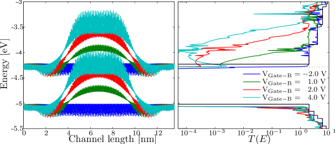
In the left part of Fig. 7 we present the total self-consistent potential induced by the three gates on the carbon atoms in the CNT over the full extension of the device. For each configuration of the gate potentials the electrostatic potential is shown twice, i.e., by two curves with the same color displaced relative to each other with the energy of the valence band and conduction band edge, respectively. In this way the curves not only represent the electrostatic potential of the device, but also the position of the valence and conduction band edges.
Along with this, in the right part of Fig. 7, we show the corresponding transmission spectrum , for four gate potentials eV, 1.0 eV, 2.0 eV, and 4.0 eV. When eV the nanotube is largely unpertubed by the gate and the transmission coefficient is close to an ideal (8,4) CNT. We note that this is in agreement with ab initio calculations by Nardelli et. al.,Nardelli et al. (2001) which found that a two terminal (5,5) CNT device in a similar contact geometry showed a nearly ideal conductance spectrum. In addition, the calculated band gap of the (8,4) nanotube is 0.81 eV, which is in good agreement with the value of 0.96 eV obtained from ab initio density-functional calculations in the generalized gradient approximation.Zhao et al. (2004)
From Fig. 7 we see how the bands are shifted upwards by an increasing amount as the Gate-B potential is turned up. To begin with, e.g., for eV, this results in lower conduction since the conduction band bends away from the Fermi level and the Fermi energy electrons need to tunnel through the central region. When the gate voltage is at eV, the valence band almost reaches the conduction band in which case BTB tunneling becomes possible. By increasing the gate voltage further, more bands become available for BTB tunneling and the effect is visible as a steady increase in the calculated transmission just above the Fermi level.
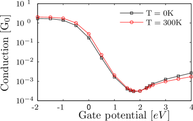
The results for the Fermi level transmission corresponding to the unit conduction , are displayed with the black curve in Fig. 8. It shows an initial conductance for V of the order of one, a subsequent drop by four orders of magnitude around V, and a final increase of one order of magnitude towards V. We also display the results for the room temperature conductance(red curve), which can be obtained from
| (24) |
The two conduction curves are similar, showing that the device is operating in the tunneling regime rather than the thermal emission regime.
We next briefly comment on the comparison of the simulation with the experiment of Appenzeller et al.. Appenzeller et al. (2004) In both cases the conduction curves have two branches, which we denote Field Emission (FE) and Band to Band Tunneling (BTB). Initially, the conduction decreases with applied gate potential due to the formation of a barrier in the central region, this is the FE regime. For larger biases the conduction increases again due to BTB tunneling, this is the BTB regime. The experimental device display thermal emission conduction and shows a corresponding subthreshold slope, , of mV/dec in the FE regime. The theoretical device, on the other hand, display tunneling conduction and has mV/dec in the FE regime. In the BTB regime, the theoretical device has mV/dec, while the experimental device show mV/dec.
The very different behavior is due to the short channel length of the theoretical device. The central barrier has a length of nm, and at this length the electron can still tunnel through the barrier. We see that the short channel length not only affects the subthreshold slope of the FE regime, but also strongly influence the BTB regime. Work are in progress for a parallel implementation of the methodology, which will make it feasible to simulate larger systems, and thereby investigate the transition from the tunnelling to the thermal emission regime.
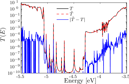
All the above results have been calculated with the modified WFM method using parameters and . Thus, the results presents a non-trivial application of the new method. To verify the transmission results in Fig. 7 we present a comparison with the standard WFM method in Fig. 9. The figure shows that the transmissions curves are identical to about three significant digits. The CPU time required for calculating a complete transmission spectrum for Fig. 7 is ( hours), while the corresponding calculation presented in Fig. 9 with the standard WFM method took ( hours). Thus, the overall time saving achieved with the new method was therefore more than an order of magnitude. The results in Table 1 indicate that similar timesavings can be expected for other systems with non-trivial electrodes.
V Summary
We have developed an efficient approach for calculating quantum transport in nano-scale systems based on the WFM scheme originally proposed by Ando in reference [Ando, 1991]. In the standard implementation of the WFM method for two-probe systems, all bulk modes of the electrodes are required in order to represent the transmitted and reflected waves in a complete basis. By extending the central region of the two-probe system with extra electrode principal layers, we are able to exclude the vast majority of the evanescent bulk modes from the calculation altogether. Our final algorithm is therefore highly efficient, and most importantly, errors and accuracy can be closely monitored.
We have applied the developed WFM algorithm to a CNTFET in order to study the mechanisms of band-to-band tunneling. The setup was inspired by reference [Appenzeller et al., 2004], and the calculation display features also observed in the experiment, however, due to the short channel length the theoretical device operates in the tunneling regime, while the experimental device operates in the thermal emission regime.
By measuring the CPU-times for calculating transmission spectra of the CNTFET two-probe system and comparing to the cost of the standard WFM method we have observed a speed-up by more than a factor of 10. We see similar speed-up for other non-trivial systems. We therefore believe that this is an ideal method to be used with ab-initio transport schemes for large-scale simulations.
Acknowledgements.
This work was supported by the Danish Council for Strategic Research (NABIIT) under grant number 2106–04–0017, “Parallel Algorithms for Computational Nano–Science”.References
- Datta (2005) S. Datta, Quantum Transport: Atom to Transistor (Cambridge University Press, Cambridge, UK, 2005).
- Brandbyge et al. (2002) M. Brandbyge, J.-L. Mozos, P. Ordejón, J. Taylor, and K. Stokbro, Phys. Rev. B 65, 165401 (2002).
- Büttiker et al. (1985) M. Büttiker, Y. Imry, R. Landauer, and S. Pinhas, Phys. Rev. B 31, 6207 (1985).
- Meir and Wingreen (1992) Y. Meir and N. S. Wingreen, Phys. Rev. Lett. 68, 2512 (1992).
- Reed et al. (1997) M. A. Reed, C. Zhou, C. J. Muller, T. P. Burgin, and J. M. Tour, Science 278, 252 (1997).
- Faleev et al. (2005) S. V. Faleev, F. Léonard, D. A. Stewart, and M. van Schilfgaarde, Phys. Rev. B 71, 195422 (2005).
- Pomorski et al. (2004) P. Pomorski, C. Roland, and H. Guo, Phys. Rev. B 70, 115408 (2004).
- Gokturk (2005) H. S. Gokturk, in Nanotechnology, 2005. 5th IEEE Conference on (2005), vol. 2, pp. 677–680.
- Stilling et al. (2006) M. Stilling, K. Stokbro, and K. Flensberg, in NSTI Nanotech 2006 Technical Proceedings (2006), vol. 3, p. 39.
- Nitzan and Ratner (2003) A. Nitzan and M. A. Ratner, Science 300, 1384 (2003).
- Di Ventra et al. (2000) M. Di Ventra, S. T. Pantelides, and N. D. Lang, Phys. Rev. Lett. 84, 979 (2000).
- Stokbro et al. (2003) K. Stokbro, J.-L. Mozos, P. Ordejon, M. Brandbyge, and J. Taylor, Comp. Mat. Sci. 27, 151 (2003).
- Lang and Avouris (2000) N. D. Lang and P. Avouris, Phys. Rev. Lett. 84, 358 (2000).
- Larade et al. (2001) B. Larade, J. Taylor, H. Mehrez, and H. Guo, Phys. Rev. B 64, 075420 (2001).
- Khomyakov and Brocks (2004) P. A. Khomyakov and G. Brocks, Phys. Rev. B 70, 195402 (2004).
- Ando (1991) T. Ando, Phys. Rev. B 44, 8017 (1991).
- Khomyakov et al. (2005) P. A. Khomyakov, G. Brocks, V. Karpan, M. Zwierzycki, and P. J. Kelly, Phys. Rev. B 72, 035450 (pages 13) (2005).
- Brocks et al. (2007) G. Brocks, V. M. Karpan, P. J. Kelly, P. A. Khomyakov, I. Marushchenko, A. Starikov, M. Talanana, I. Turek, K. Xia, P. X. Xu, et al., -Newsletter 80, 144 (2007), URL http://www.psi-k.org/newsletters/News_80/newsletter_80.pdf.
- Sørensen et al. (2008) H. H. B. Sørensen, P. C. Hansen, D. E. Petersen, S. Skelboe, and K. Stokbro, Phys. Rev. B 77, 155301 (2008).
- Appenzeller et al. (2004) J. Appenzeller, Y.-M. Lin, J. Knoch, and P. Avouris, Phys. Rev. Lett. 93, 196805 (2004).
- Sørensen (2008) H. H. B. Sørensen, Ph.D. thesis, Technical University of Denmark, DK-2800, Kgs. Lyngby, Denmark (2008).
- Ashcroft and Mermin (1976) N. W. Ashcroft and D. N. Mermin, Solid State Physics (Brooks Cole, 1976).
- Guinea et al. (1983) F. Guinea, C. Tejedor, F. Flores, and E. Louis, Phys. Rev. B 28, 4397 (1983).
- Lopez Sancho et al. (1985) M. P. Lopez Sancho, J. M. Lopez Sancho, J. M. L. Sancho, and J. Rubio, J. Phys. F. 15, 851 (1985).
- Krstić et al. (2002) P. S. Krstić, X.-G. Zhang, and W. H. Butler, Phys. Rev. B 66, 205319 (2002).
- Hoffmann (1963) R. Hoffmann, The Journal of Chemical Physics 39, 1397 (1963).
- Zahid et al. (2005) F. Zahid, M. Paulsson, E. Polizzi, A. W. Ghosh, L. Siddiqui, and S. Datta, J. of Chem. Phys. 123, 064707 (2005).
- (28) K. Stokbro, unpublished.
- Nardelli et al. (2001) M. B. Nardelli, J.-L. Fattebert, and J. Bernholc, Phys. Rev. B 64, 245423 (2001).
- Zhao et al. (2004) G. L. Zhao, D. Bagayoko, and L. Yang, Phys. Rev. B 69, 245416 (2004).
- Fisher and Lee (1981) D. S. Fisher and P. A. Lee, Phys. Rev. B 23, 6851 (1981).