Tunable hybridization of electronic states of graphene and a metal surface
Abstract
We present an approach to monitor and control the strength of the hybridization between electronic states of graphene and metal surfaces. Inspecting the distribution of the band in a high-quality graphene layer synthesized on Ni(111) by angle-resolved photoemission, we observe a new ”kink” feature which indicates a strong hybridization between and d states of graphene and nickel, respectively. Upon deposition and gradual intercalation of potassium atoms into the graphene/Ni(111) interface, the ”kink” feature becomes less pronounced pointing at potassium mediated attenuation of the interaction between the graphene and the substrate.
Since the discovery of two–dimensional meta–stable graphene sheets geim07-review much research has been devoted to explore its electronic properties because it is most suitable for nanoelectronic devices with high electronic mobilities of (15000 novoselov06-graphite at room temperature) and can be lithographically patterned successfully berger07-graphene . The electronic structure of isolated graphene in the vicinity of the Fermi level (EF) is that of a zero -gap semiconductor, where the bare bands are linear and the density of states at EF equals zero. These exotic properties give rise to a number of fascinating effects such as quasi relativistic Klein tunneling geim06-kleinparadox , an anomalous quantum Hall effect novoselov06-graphite and a node in the optical absorption close to EF n950 . Strong renormalizations of the quasi–particle bands due to electron–electron alex06-correlation , electron–phonon takahashi07-prl and electron–plasmon rotenberg06-graphite interactions were observed by angle–resolved photoemission (ARPES) in pristine graphite and graphene on SiC. ARPES spectra of graphite single crystals are not affected by substrate (sample holder) interactions since they exceed in thickness. With the graphene layer, however, the SiC substrate interacts and transfers electrons to the band of graphene. This charge transfer occurs according to a rigid band shift model since there is no hybridization of the Si and the C orbitals.
The situation is changed dramatically in the case of graphene/metal systems. Strong hybridization of electronic states and charge transfer between graphene and the metal substrate modify the band structure of graphene. In this respect intercalation of foreign atoms into those systems is a key point, which can help to understand and separate these two competing phenomena. It has already been demonstrated that graphene grown epitaxially on Ni(111) shelton74-graphene ; oshima94-graphene has an electronic structure quite different to pristine graphene for two reasons. First, the Ni and C orbitals are elongated along the direction perpendicular to the graphene sheet and have a large overlap. Second, the interplane distance between the graphene layer and the Ni(111) surface is significantly smaller than in bulk graphite. Low energy electron diffraction (LEED) measurements carried out on graphene/Ni(111) system suggest that one atom of the graphene unit cell is located on above the topmost Ni layer and the other carbon atom is located on top of hollow sites oshima97-grapheneposition . This structural assignment is consistent with the observation of a gap opening at the point (or Dirac point) at the Brillouin zone (BZ) corner oshima94-graphene which indicates that the two atoms in the unit cell are situated at nonequivalent positions on the Ni(111) surface. Also, it was found experimentally the K atoms deposited onto the graphene surface penetrate to the graphene/Ni(111) interface already at room temperature oshima94-graphene . This approach offers an appealing possibility to control the degree of hybridization between Ni and C orbitals which is quite important and strongly motivated by requirements of precise control and functionalization of graphene based nanostructures. Although a few works oshima94-graphene ; molo01-graphene have been conducted with the aim to study modifications of the electronic structure of graphene on metallic substrates, the detailed description of the hybridization phenomena in graphene/metal interfaces is still lacking. Exploiting this effect, however allows to explore charge transfer in the crossover regime between hybridization and the simple rigid band model.
In this contribution we present a comprehensive and systematic ARPES study of the evolution of the electronic band structure of graphene layer on Ni(111) under gradual penetration of K atoms to the graphene/Ni(111) interface. We show that due to strong hybridization graphene and Nickel states the band is pushed downwards by the Ni bands, revealing new ”kink” feature. However, upon gradual deposition of K atoms the ”kink”-like structure becomes less pronounced indicating K-mediated attenuation of the hybridization between the graphene and the metallic substrate. In order to describe the changes in the electronic structure quantitatively, we perform calculations on the tight–binding (TB) level. The experiments were performed using a photoemission spectrometer equipped with a Scienta SES-200 hemispherical electron-energy analyzer, a high-flux He-resonance lamp (Gammadata VUV-5010) in combination with a grating monochromator and an X-ray source. All valence PE spectra were acquired at a photon energy of h=40.8 eV (He II) with an angular resolution of 0.3∘ and a total-system energy resolution of 50 meV. The samples were measured at room temperature. X–ray photoelectron spectroscopy (XPS) was applied in order to estimate the K /C intensity ratio (K/C) as well as the quality of the samples. The XPS spectra were obtained at a photon energy of 1486.6 eV (Al K). Cleanliness and high crystalline quality of the prepared structures were cross checked by LEED.
 |
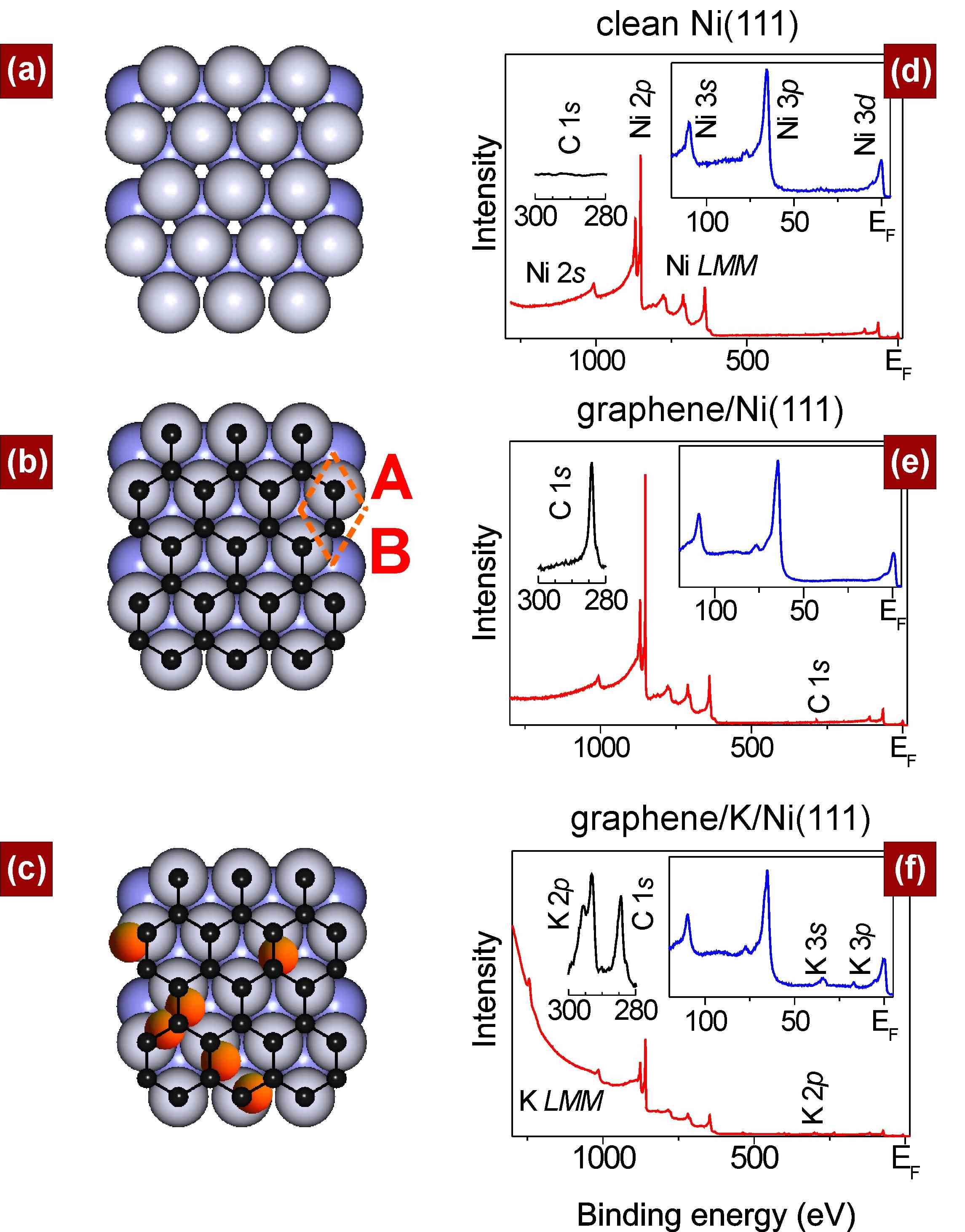
Fig. 1(a)–(c) show the sample preparation schematically. In the beginning the electronic and crystalline structures of the clean Ni(111) surface are inspected. Subsequently, we perform chemical vapour deposition (CVD) of propylene in order to grow the graphene layer catalyzed by Ni(111) oshima94-graphene ; molo01-graphene . After that we evaporate potassium onto the sample. Fig. 1(d)–(f) displays XPS spectra taken at each stage of the experiment. Inspecting these spectra briefly, it is obvious that appearance of the graphene layer is accompanied by a sharp peak at 285 eV BE due to electron emission from the core-level of carbon.
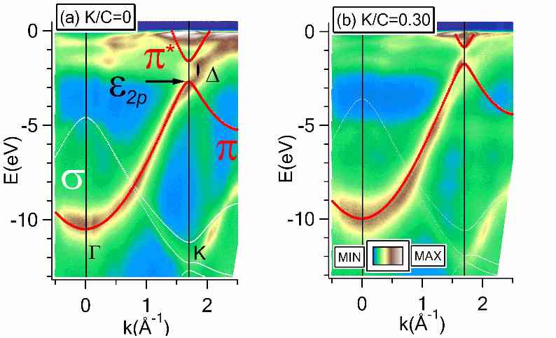
In Fig. 2 the electronic structure of pristine and potassium doped graphene/Ni(111) is shown. Inspecting the topology of the band dispersions one can make the following general observations: (i) for K/C=0 the band structure is shifted down in binding energy by 2.7 eV with respect to what is expected from theory for an isolated graphene monolayer; (ii) for K/C=0.30 the intensity from Ni states with a flat dispersion close to the Fermi level is suppressed and the and bands at point move up in BE. Thus for the K/C=0.30 the observed graphene electronic bands are that of a doped graphene layer with a rather small interaction with the Ni substrate. The first point is explained by a strong covalent bonding between the graphene layer and the Nickel surface. The second point indicates that intercalated potassium atoms gradually extends the interlayer distance without affecting the morphology of the graphene monolayer. This decreases the overlap between wave functions of C and Ni states oriented perpendicular to the surface, decreasing the strong interlayer interaction of graphene and the substrate. The proof for intercalation of potassium to the Nickel/graphene interface comes from the intensity ratio of the photoemission from states of graphene to states of Ni(111). We observe a strong increase of this intensity ratio. This clearly indicates penetration of potassium atoms to the graphene/nickel interface. Since we do not observe an intercalant band from the potassium 4 electrons we conclude that we have complete charge transfer of one electron per potassium atom. The amount of charge transfer is strongly dependent on the carbon material and the intercalant atom and for different systems one might expect a different degree of charge transfer rukola08-kc8lda .
In order to describe the electronic structure of the intercalated graphene monolayer we perform TB calculations of the and bands taking into account nearest neighbor interactions s617 . In order to describe the influence of the Ni(111) surface and intercalated K ions on the electronic structure of the graphene monolayer we adjusted the values of the on–site C energies for the and atoms of the graphene unit cell [see Fig. 1(b)], i.e. we employed the rigid band shift model. The band Hamilton and overlap matrices are given by
| (1) |
and
| (2) |
respectively. Here we use
| (3) |
| K/C ratio | 0 | 0.17 | 0.3 | 0.69 |
|---|---|---|---|---|
| -2.7 | -2.4 | -1.6 | -1.5 | |
| 0.9 | 0.8 | 0.9 | 0.8 | |
| 3.2 | 3.2 | 3.4 | 3.3 |
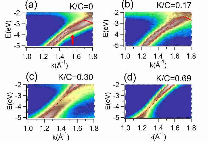
At the point of the two–dimensional Brillouin zone of graphene we obtain and thus the Eigenvalues at are given by the diagonal elements of , i.e. and , respectively. The electronic band structure is given by solving the Schrödinger equation , where and denote the Eigenvalues and wave function coefficients, respectively. We managed to reproduce the topology of the graphene electronic states by fitting , and the overlap () to the experimental data. Other parameters related to the bands such as the on–site energy and overlap need not to be changed since the hybridization of states of graphene with d-states of the Ni(111) surface is rather weak. The values of the parameters used in the TB calculation are summarized in Table 1. Our calculations demonstrate that with proceeding potassium intercalation decreases distinctly by 1.2 eV in direction of EF. At the last stage of the experiment, i.e. for complete intercalation, was found to be at 1.5 eV below EF. The values for and do not reveal significant changes with increasing K/C ratio. Now, let us take a closer look at the shape of the band between and points shown in Fig. 3. Obviously, in the vicinity of the point the dispersion of the experimentally derived band is accurately reproduced by the TB calculation. However, close to the point this agreement is strongly affected by the value of the K/C ratio. For the case of the pristine graphene/Ni(111) structure (K/C=0) the ”kink” shape of this band is clearly visible. The BE of the ”kink” is too high, about 3.5 eV, to attribute it to electron-plasmon or electron-phonon interactions. Accurate consideration of this picture suggests that the band is pushed downwards by the Ni bands. Thus one can suppose that the ”kink” is a product of hybridization between graphene and nickel states.
Details of the dispersion of band close to the point where the ”kink” was monitored for K/C=0 are shown in Fig. 3 as a function of the K/C ratio. Note that with increasing amount of intercalated potassium atoms the strength of the ”kink” is gradually reduced. For the case of K/C=0.3 one can distinguish a second component of the band. This fact may be interpreted as follows: there are certain sample positions where potassium intercalates already underneath the graphene, reducing its interaction with the Ni(111) surface. Thus, at this stage both phases, a strongly hybridized and an intercalated graphene layer with small substrate interaction, coexist. For the case K/C=0.69 the ”kink” disappears and the usual steep slope behavior of the band appears. Further increasing K/C does not reveal significant changes.
 |
 |
We discuss now the present experimental and theoretical results. The derived fit parameters for the bands imply the following physical interpretation: by intercalation of potassium atoms to the graphene/Ni(111) interface, the strong hybridization between C and Ni orbitals is weakened. Furthermore, when the graphene layer is lifted up, it is no longer attached to the Ni(111) surface and the lattice constant of graphene might relax to a slightly lower value. These two effects are expected to decrease and increase . While the increase of is clearly observable, the increase of is in the range of the experimental error. The reason for this is probably that the difference in lattice constants is too small (1.42 for C-C and 1.44 for Ni-Ni) to produce a noticeable change in . The fact that does not change over the whole doping range is quite different to the case of bilayer graphene. In the case of bilayer graphene on SiC the gap is equal to the doping dependent difference in the on–site energy for the two layers rotenberg06-graphite_bilayer . In the case of a monolayer, the gap is given by the difference of the on–site energy for the and atom in the graphene unit cell. Since and atoms occupy non–equivalent sites on the Ni(111) surface [see Fig. 1(b)] this can be easily understood for the case of K/C=0. For higher doping, the absence of a change in the gap might thus be related to a superstructure of the potassium atoms on the Ni(111) surface.
The valence bandwidth is given by and the experimentally derived values for in this work are about 20% larger than the LDA derived ones alex06-correlation . We thus conclude that the increase in the experimental bandwidth is due to electron–electron correlations, similar to the case of graphite alex06-correlation . The valence bandwidth of graphene is not affected by the fact that the graphene monolayer is hybridized with the metal surface since it is identical with the graphite bandwidth. Such a result is surprising since one might expect that the graphene/metal interface enhances the screening of carriers in graphene and thus leads to a better agreement with the LDA. Hopefully, these new findings will stimulate further theoretical considerations.
Concerning other spectroscopic techniques it would be interesting to probe the electronic structure of pristine and functionalized graphene monolayers by optical spectroscopy such as resonance Raman. The (double) resonance Raman process involves transitions c887 and in order to fulfill the resonance condition it is clear that the laser energy h must be larger than . From ARPES experiment we can predict the resonance condition which yields h=4.5 eV for K/C=0 and h=2.2 eV for K/C=1.02 as a lower limit for the laser energy in resonance Raman measurements.
Finally, we would like to add one more point. It is reasonable to anticipate that alkali-metal intercalated high-quality graphene layers on Ni(111) surfaces bring up the opportunity to use them for the preparation of top quality graphene layers on different substrates. Since the intercalation liberates the graphene from strong covalent bonding with Ni(111), it would be feasible to peel off intercalated graphene from the substrate.
In summary, we have investigated modifications of the electronic structure of the graphene layer on the Ni(111) substrate upon gradual intercalation of potassium metal. We found that the hybridization strength between graphene and Ni states can be monitored successfully by the ”hybridization” kink of the band distribution while the charge transfer follows a rigid band shift model in perfect agreement with results of TB calculations. We anticipate that the graphene/Ni(111) structure could be used successfully as a model system capable to provide valuable insight into the mechanisms of electron correlations and many-body interactions in solids.
A.G. acknowledges a Marie Curie Individual Fellowship (COMTRANS) from the European Union. D.V. acknowledges the Deutsche Forschungsgemeinschaft (SFB 463) for projects TP B4 and TP B16. Fruitful discussions with Thomas Pichler, Martin Knupfer, Clemens Laubschat and Serguei Molodtsov are gratefully acknowledged.
References
- (1) A. Geim et al. Nature Mat. 6, 183 (2007).
- (2) K. Novoselov et al. Science 306, 666 (2004).
- (3) C. Berger et al. Surface Science 108, 19912 (2004).
- (4) M. I. Katsnelson et al. Nature Phys. 2, 620 (2006).
- (5) A. Grüneis et al. Phys. Rev. B 67, 165402 (2003).
- (6) A. Grüneis et al. Phys. Rev. Lett. 100, 037601 (2008).
- (7) K. Sugawara et al. Phys. Rev. Lett. 98, 036801 (2007).
- (8) A. Bostwick et al. Nature Phys. 3, 36 (2007).
- (9) J. Shelton et al. Surface Science 43, 433 520 (1974).
- (10) A. Nagashima et al. Phys. Rev. B 50, 17487 (1994).
- (11) Y. Gamo et al. Surface Science 374, 61 (1997).
- (12) Y. Dedkov et al. Phys. Rev. B 64, 35405 (2001).
- (13) K. Rytkönen et al. Phys. Rev. B 75, 075401 (2007).
- (14) R. Saito et al. Physical Properties of Carbon Nanotubes. Imperial College Press, London (1998).
- (15) T. Ohta et al. Science 313, 951 (2006).
- (16) R. Saito et al. Phys. Rev. Lett. 88, 027401 (2002).