Nano-Engineering Defect Structures on Graphene
Abstract
We present a new way of nano-engineering graphene using defect domains. These regions have ring structures that depart from the usual honeycomb lattice, though each carbon atom still has three nearest neighbors. A set of stable domain structures is identified using density functional theory (DFT), including blisters, ridges, ribbons, and metacrystals. All such structures are made solely out of carbon; the smallest encompasses just 16 atoms. Blisters, ridges and metacrystals rise up out of the sheet, while ribbons remain flat. In the vicinity of vacancies, the reaction barriers to formation are sufficiently low that such defects could be synthesized through the thermally activated restructuring of coalesced adatoms.
Carbon is a fundamental material for nano-engineering. Three dimensional graphite, one-dimensional nanotubes, zero-dimensional buckyballs, and now two-dimensional graphene are all being investigated intensely to this end. The latter, recently created experimentally for the first time novoselov2005 ; zhangYB2005 , is the first stable two-dimensional solid state lattice material. Fundamental aspects of graphene include the room-temperature quantum Hall effect and an effective description by a Dirac equation geim2007 . Graphene has significant applications in electronics schedin2006 ; silvestrov2007 ; green2007 , and is even predicted to replace silicon in future solid state devices geim2007 . Many of these applications require cutting sheets of graphene precisely in order to localize charge, among other effects. We propose an alternative method of patterning graphene without cuts of any kind, which can be adapted to many applications. The key to this method is controlled placement of groups of defects, called defect domains.
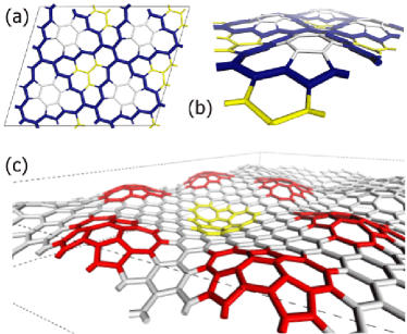
In this Letter, we demonstrate that a complex, stable landscape of defect domains can be monolithically nano-engineered from graphene to make arbitrary structures. An example of a defect domain which stands up out of the graphene plane is shown in Fig. 1(a)-(b). Such defect blisters in graphene can be generated through the coalescence of adatoms in the vicinity of vacancies (Fig. 1(c)). Defect ridges can be constructed as an alignment of blisters and their two-dimensional patterning results in defect metacrystals. Planar, defect ribbons may also be synthesized as shown in Fig. 1(d). These structures, in particular, may be viewed as being spliced-in pieces of a carbon allotrope known as haeckelite terrones2000 . Figure 1(e)-(f) show how haeckelite symmetry considerations may be used to predict energetically favorable defect domain geometries. We use density functional theory (DFT) to study stability, scalability, and other key physical properties of these materials. DFT has been applied successfully to magnetism in graphene nano-islands fernandezJ2007 , the effect of substrates varchonF2007 , and transport in doped graphene nanoribbons martins2007 ; DFT is also used for carbon nanotubes chandrasekera2007 ; borstnika2005 and other carbon structures hamm2007 .
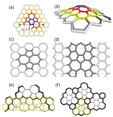
Defects have been observed in graphene geim2007 ; hashimoto_2004 and are expected to play a key role in the functional properties of working materials lu_2004 . Among the simplest and more easily fabricated of these is the Stone-Wales defect, wherein the rotation of a single pair of carbon atoms creates adjacent pairs of pentagonal and heptagonal rings stone_1986 , as shown in Fig. 1(c). Such defects can be introduced intentionally using electron radiation and imaged using Transmission Electron Microscopy (TEM) hashimoto_2004 . Electron radiation also causes the formation of adatom/vacancy pairs which subsequently separate and move across the graphene lattice hashimoto_2004 . DFT analysis krasheninnikov2004 estimates the adatom migration barrier to be 0.45 eV with a jump frequency of , while the barrier to vacancy migration is estimated to be 1.7 eV with a jump frequency on the same order as for adatoms elbarbary2003 . Electron radiation can therefore be used to generate adatoms and vacancies which have been observed to rearrange themselves to form more complex defect structures hashimoto_2004 .
Domains over which similar defect structures are periodically replicated are known as haeckelite terrones2000 , as shown in Fig. 1(f). Tight binding molecular dynamics studies suggest that small regions of these carbon allotropes may be induced within graphene through the coalescence of four single vacancies lee_2006 . In principle, entire sheets and tubes of haeckelite can be synthesized which, even without experimental realization, have already generated potential applications mpourmpakis_2006 . We focus on the simpler notion of localized defect structures which are minimally extended beyond Stone-Wales defects. We initially treat defects composed of ribbons and patches of haeckelite and then consider a new fundamental building block which we term an Inverse Stone-Wales defect.
All calculations were performed with the real-space, numerical atomic orbital, DFT code, DMOL JChemPhys.113.7756 . A norm conserving, spin unrestricted, semi-core pseudopotential approach was employed with electron exchange and correlation accounted for using the Perdew-Wang generalized gradient approximation (GGA) PhysRevB.45.13244 . Periodic boundary conditions were employed and vacuum slabs were used to isolate the replicated graphene layers. As a check on the method, the ground state energy of C60, i.e., a buckyball, was estimated to be 384 meV/atom above that of graphene, consistent with a literature value of 380 meV/atom terrones2004 . Likewise, a single Stone-Wales defect was estimated to have a formation energy of 5.08 eV when embedded within a 144-atom graphene supercell; this compares well with an estimate of 4.8 eV from the literature li:184109 .
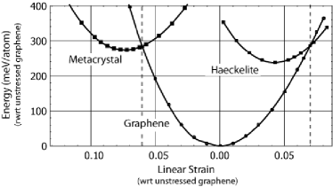
We begin with defect structures constructed from patches of haeckelite terrones2000 . The H5,6,7 variant with hexagonal symmetry was chosen over rectangular and oblique allotropes. This is the most stable of the three variants. We find a ground state energy estimate for H5,6,7 of 229 meV/atom above graphene. This is close to the literature value of 246 meV/atom and notably lower than that of C60 terrones2004 . H5,6,7 is less dense than graphene: it has 0.369 atoms/Å2, compared to 0.380 atoms/Å2 for graphene. Haeckelite can therefore be formed by the removal of carbon atoms or in settings in which the graphene sheet can expand. For instance, a 20-atom periodic cell of this carbon allotrope can be formed through the addition of two carbon atoms to a Stone-Wales defect followed by lateral dilation. The energy barrier is estimated to be 1.8 eV per cell. Such restructuring should be aided by straining the graphene. DFT calculations support this and indicate that the stability exchange occurs at a linear strain of 0.07, as shown in Fig. 2. The analysis also determined uni-axial elastic constants for graphene and haeckelite of 1.13 GPa and 1.20 GPa, respectively. The first number is consistent with experimental measurement of 1.06 GPa PhysRevB.7.4527 , while the second indicates that haeckelite is 6% stiffer than graphene.
Two types of approximately coherent interfaces between graphene and H5,6,7 can be identified by inspection and are shown in Fig. 1(e)-(f). A linear haeckelite strain of gives averaged coherence along the symmetry boundaries shown in Fig. 1(e), while triangular patches of haeckelite are approximately coherent without applying any dilation, as illustrated in Fig. 1(f). With these lines as a guide, haeckelite can be spliced into a graphene sheet and vice-versa. A strip of haeckelite spliced into graphene along adjacent, linear coherency lines has a planar ground state, as shown in Fig. 1(d), where the dashed lines indicate the periodicity of our simulation. On the other hand, splicing a triangular tile from Fig. 1(f) into graphene causes a ground state blister to form, as shown in Fig. 1(a)-(b). The converse, a triangular graphene patch within haeckelite, results in a planar structure.
The concept of a defect blister creates a natural way to extend graphene out of the plane. A formation energy of 6.07 eV was determined for the blister illustrated in Fig. 1(a)-(b), using a 202-atom supercell. This is approximately 1 eV higher than the Stone-Wales defect. A Hessian analysis wilson1955 on a smaller supercell indicates that such haeckelite-based defect blisters are linearly stable. This is consistent with the stability observed in a room temperature quantum molecular dynamics simulation, which we also performed.
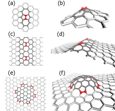
We now turn to an even simpler defect domain structure not based on Haeckelite, and explicitly describe its reaction pathway. While haeckelite-based defect blisters amount to the substitution of a pair of atoms for a hexagonal ring (Fig. 1(f)), a narrower structure can be formed by inserting two atoms on opposing faces of an existing hexagon as shown in Fig. 3(a)-(b). This results in pairs of pentagons and heptagons that we refer to as an Inverse Stone-Wales defect (compare to Fig. 1(c)). A 16-atom blister results with a footprint of Åand a height of 2.1 Å. A formation energy of 6.20 eV was determined using a 200-atom supercell, nearly the same energy as that for the larger haeckelite blister. A series of Inverse Stone-Wales blisters can be aligned to form a corrugated ridge of nearly arbitrary contour (Fig. 3(c)-(d)), a monolithic analog of carbon nanotubes formed from C60 molecules rodriguez2004 . Such structures may hold utility in guiding charge transport on graphene. Further, the creation of closed contours results in extended blisters of pure graphene enclosed by a ring of Inverse Stone-Wales defects. (Fig. 3(e)-(f)).
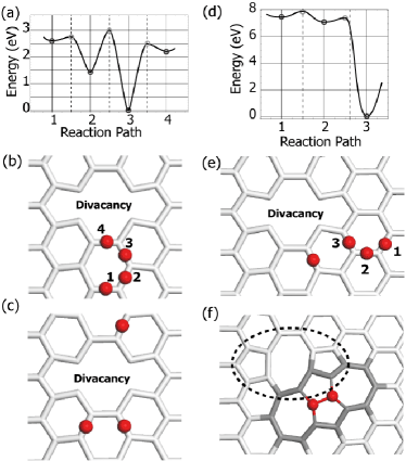
The synthesis of defect structures may be facilitated by electron radiation and the resulting collection of adatoms and vacancies hashimoto_2004 . The formation energy for a single vacancy was calculated to be 7.63 eV, consistent with experimental estimates thrower1978 , and therefore has the potential to provide a large driving force for restructuring events within its horizon. The formation energy of a vacancy/adatom pair, the planar analog of a Frenkel defect, is 14.13 eV. Di-vacancy formation energy was calculated to be 8.08 eV. In addition, re-structuring within such a low dimensional system is more easily carried out than in bulk since vacancies facilitate significant low energy distortions of the local lattice. To explore this, a hybrid linear synchronous transit/quadratic synchronous transit (LST/QST) transition state search algorithm govind2003 was used to construct a reaction pathway for the approach of a single adatom to a di-vacancy (Fig. 4). Adatoms hop between adjacent bridge sites, and a barrier of 0.52 eV was identified for jumps in pure graphene, consistent with an estimate of 0.45 eV obtained elsewhere krasheninnikov2004 . However, the di-vacancy attracts adatoms to positions that are one hop removed from its periphery (position 3 in Fig. 4(b)), and the associated barriers can be overcome by thermal fluctuations at modest temperatures. These are precisely the bridge sites at which adatoms are observed experimentally (Fig. 4(c)) hashimoto_2004 . The reaction energies in Fig. 4(a) are eV, eV, and eV, while the reaction barriers are eV, eV, and eV.
Two adatoms are required to synthesize an Inverse Stone-Wales blister. So a second transition state analysis was carried out wherein one adatom jumped towards another located at a low energy site on the periphery of the di-vacancy, as shown in Fig. 4(e)-(f). As indicated in the figure, the reaction barriers can be overcome by thermal fluctuations at modest temperatures and result in a blister. The reaction energies are eV and eV, while the reaction barriers are eV and eV. Subsequent vacancy migration or elimination would leave the stand-alone blister shown in Fig. 3(a)-(b).
Localized defect domains are of interest in their own right, but patterned arrangements of them may endow graphene sheets with novel metacrystalline properties. Within such a paradigm, blisters represent meta-atoms with either up or down polarity. A mono-sized, mono-polarity, ground state, metacrystal is shown in Fig. 5(a)-(b). The associated mechanical response given in Fig. 2 indicates that it has a density greater than that of graphene. The ground state energy is only 274 meV/atom above that of graphene and is surprisingly close to the ground state energy of pure haeckelite, which is 229 meV/atom above graphene. This suggests that the metacrystals are more energetically stable than C60; the latter has an analogous energy of 384 meV/atom. The elastic stiffness of the metacrystal is 1.08 GPa in uni-axial tension, somewhat less that either graphene or haeckelite. One possibility for the experimental realization of defect metacrystals in graphene is interference patterns of electrons in the near field of a diffraction grating croninAD2006 . Such a system has been demonstrated at the 100 nm scale already and has the potential to be reduced to the 10 nm scale. Metacrystals can also be made with larger blisters or even blisters of alternating size. Thus one can consider a “periodic table” of meta-atoms, creating a variety of 2D metacrystals of arbitrary lattice and crystal structure.
In conclusion, we have described a new method to achieve monolithic nano-engineering of graphene via defect domains. These structures can take the form of blisters, ribbons, and ridges. We showed that such objects are linearly stable and can be arranged in arbitrary patterns, leading to a metacrystal. The smallest defect domain, referred to as an Inverse Stone-Wales defect, consists of only 16 atoms, and the associated energy is approximately 1 eV higher than a simple Stone-Wales defect. Di-vacancies were shown to attract adatoms to their periphery and a thermally activated path was identified for blister synthesis. Defect domains may offer technological applications associated with the confinement and transport of charge, as we will investigate in future work.
We acknowledge useful discussions with James Bernard, David Wood, and David Wu. LDC was supported by the National Science Foundation under Grant PHY-0547845 as part of the NSF Career program.
References
- (1) K. S. Novoselov et al., Nature 438, 197 (2005).
- (2) Y. B. Zhang, Y. W. Tan, H. L. Stormer, and P. Kim, Nature 438, 201 (2005).
- (3) A. K. Geim and K. S. Novoselov, Nature Materials 6, 183 (2007).
- (4) F. Schedin et al., e-print cond-mat/0610809 (2006).
- (5) P. G. Silvestrov and K. B. Efetov, Phys. Rev. Lett. 98, 016802 (2007).
- (6) K. Greene, Technology Review (2007).
- (7) H. Terrones et al., Phys. Rev. Lett. 84, 1716 (2000).
- (8) J. Fernández-Rossier and J. J. Palacios, Phys. Rev. Lett. 99, 177204 (2007).
- (9) F. Varchon et al., Phys. Rev. Lett. 99, 126805 (2007).
- (10) T. B. Martins, R. H. Miwa, A. J. R. da Silva, and A. Fazzio, Phys. Rev. Lett. 98, 196803 (2007).
- (11) K, Chandrasekera and S, Mukherjee, Comp. Mat. Sci. 40, 147 (2007).
- (12) U. Bor tnika, M. Hodo ceka, D. Jane ica and I. Lukovitsb, J. Chem. Phys. 411, 384 (2005).
- (13) M. T. Lusk and N. Hamm, Phys. Rev. B 76, 125422 (2007).
- (14) A. Hashimoto et al., Nature 430, 870 (2004).
- (15) X. Lu, Z. Chen, and P. Schleyer, J. Am. Chem. Soc. 127, 20 (2005).
- (16) A. Stone and D. Wales, Chem. Phys. Lett. 128, 501 (1986).
- (17) A. Krasheninnikov et al., Carbon 42, 1021 (2004).
- (18) A. A. El-Barbary et al., Phys. Rev. B 68, 144107 (2003).
- (19) G.-D. Lee et al., Phys. Rev. B 74, 245411 (2006).
- (20) G. Mpourmpakis, G. E. Froudakis, and E. Tylianakis, App. Phys. Lett. 89, 233125 (2006).
- (21) B. Delley, J. Chem. Phys. 113, 7756 (2000).
- (22) J. P. Perdew and Y. Wang, Phys. Rev. B 45, 13244 (1992).
- (23) X. Rocquefelte et al., Nano Lett. 4, 805 (2004).
- (24) L. Li, S. Reich, and J. Robertson, Phys. Rev. B 72, 184109 (2005).
- (25) A. A. Ahmadieh and H. A. Rafizadeh, Phys. Rev. B 7, 4527 (1973).
- (26) E. Wilson, J. Decius, and P. Cross, Molecular Vibrations (Dover, New York, NY, 1955).
- (27) J. A. Rodríguez-Manzo, F. López-Urias, M. Terrones, and H. Terrones, Nano Lett. 4, 2179 (2004).
- (28) P. A. Thrower and R. M. Mayer, Physica Status Solidi A 47, 11 (1978).
- (29) N. Govind et al., Comp. Mat. Sci. 28, 250 (2003).
- (30) A. D. Cronin and B. McMorran, Phys. Rev. A 74, 061602(R) (2006).