Subwavelength imaging of light by arrays of metal-coated semiconductor nanoparticles: a theoretical study
Abstract
Rigourous calculations of the imaging properties of metamaterials consisting of metal-coated semiconductor nanoparticles are presented. In particular, it is shown that under proper choice of geometric and materials parameters, arrays of such particles exhibit negative refractive index within the region of the excitonic resonance of the semiconductor. The occurrence of negative refractive index is predicted by the extended Maxwell-Garnett theory and confirmed by a layer-multiple scattering method for electromagnetic waves. By using the same method it is shown that within the negative refractive-index band, arrays of such nanoparticles amplify the transmitted near-field emitted while simultaneously narrow down its spatial profile leading to subwavelength resolution. The effect of material losses to the imaging properties of the arrays is also addressed.
pacs:
42.70.Qs, 42.25.Bs, 78.67.Pt, 78.67.Bf, 73.20.Mf1 Introduction
According to a recent definition [1], metamaterials are artificial materials which exhibit response characteristics that are not observed in the individual responses of its constituent materials. The most fascinating class of metamaterials are those exhibiting simultaneously negative permittivity and permeability , i.e., a negative refractive index (NRI) [2, 3]. The usual approach of designing a NRI metamaterial is to combine a ’magnetic’ sublattice (one which exhibits negative ) of miniaturized RLC circuits, e.g. split-ring resonators, with an ’electric’ one (exhibiting negative ) of thin metallic wires [4]. However, an alternative route has been recently suggested where the electric and magnetic sublattices are occupied by units of less elaborate geometry such as cylinders or spheres made from resonant materials (ionic, semiconducting or plasmonic materials) displaying high-refractive index within a specific frequency window [5, 6, 7, 8, 9, 10, 11, 12, 13, 14, 15, 16]. The magnetic activity of the cylinders/ spheres lies within the region of Mie resonances resulting from the enhancement of the displacement current inside each sphere which, in turn, gives rise to a macroscopic magnetisation of the whole structure. The electric activity is attributed to the large polarization induced to the sphere due to the giant dielectric permittivity around the resonance frequency of a given dielectric function, e.g. polariton, plasmon or exciton resonance. The above theoretical suggestions have been recently verified experimentally for arrays of dielectric particles of millimeter [17] and micrometer [18] size. Such arrays can be miniaturized to the nanometre scale in the form of nanoparticle superlattices [19].
Perhaps, the most paramount application of NRI metamaterials is their imaging property; as has been pioneered by Pendry [3] and verified experimentally, a planar slab of metamaterial with NRI can overcome the standard diffraction limit in imaging by focusing the far-field via negative refraction [20, 21] and by amplifying the near-field [22, 23, 24] by surface-plasmon excitation, a possibility which promises the realization of a perfect lens. Near-field amplification is also feasible separately for S-polarized waves in the magnetostatic limit using solely RLC circuits such as split-ring resonators and Swiss rolls [25, 26] and for P-polarized waves in the electrostatic limit using periodic structures with metallic components such as rods [27], wires [28], and spheres [29].
In this work we study the imaging properties of three-dimensional (3D) NRI metamaterials consisting of metal-coated semiconductor spheres. As has been recently shown, arrays of semiconductor spheres with strong excitonic oscillation strength (CuCl, ) can exhibit negative permeability in the visible region, around the exciton resonance [14]. In order to realize an NRI structure in the regime of negative , the array of semiconductor spheres can be (a) either combined with an array of metallic spheres (negative ) in a way that a binary NRI structure is created [8], or (b) by coating the semiconductor spheres with a metallic shell [11, 30]. The above structures have been studied by employing both effective-medium treatments [6, 12, 13] and more rigorous electromagnetic approaches [8, 11]. By exploiting the occurrence of NRI in the case of arrays of metal-coated semiconductor nanoparticles, we will show that near-field amplification along with subwavelength resolution of an image can be achieved in such structures, for both polarization modes. We will also elucidate the role of absorption which is intrinsic in the materials constituting the NRI metamaterial under study. The paper is organized as follows. In section 2 the basic theoretical tools for studying the imaging properties of arrays of spherical inclusions is presented. Section 3 applies the theory to the case of metal-coated semiconductor spheres and section 4 concludes the paper.
2 Theory
In this work, we are dealing with finite slabs of metamaterials consisting of a number of planes of spheres with the same 2D periodicity. In order to probe the imaging properties of these structures, we consider the electric field emitted by a localized source, namely, that radiated by a small, linear, infinitely thin, center-fed antenna. The antenna lies along the -axis from with current . We expand the electric field radiated by the antenna as a series of spherical waves [31]
| (1) |
are the so-called vector spherical harmonics [31] and are the spherical Hankel functions of order . , where is the velocity of light in the medium surrounding the antenna. The magnetic multipole coefficients are zero whilst the electric ones are given by [32]
| (2) |
provided that is odd and . in equation (2) denote the spherical Bessel functions. Note that the above formula is valid in the case where the antenna is much smaller than the wavelength [32], i.e., .
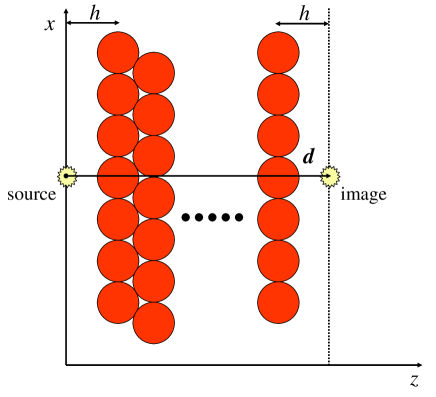
Since we wish to study the transmission of the above field through a slab of a number of periodic planes of spheres, it is advantageous to transform the field of equation (1) to a basis of plane waves consistent with the 2D periodicity of the planes of spheres. If the linear antenna is placed to the left of the slab (see the calculation setup in figure 1), then the field radiated to the right and is incident on the slab is written as (assuming the center of coordinates be located at the localized source)[33]
| (3) |
with
| (4) |
where are the two independent polarizations (polar and azimuthal) which are normal to the wavevector [34, 35, 36]
| (5) |
The vectors denote the reciprocal-lattice vectors corresponding to the 2D periodic lattice of the plane of spheres and is the reduced wavevector which lies within the Surface Brillouin Zone (SBZ) associated with the reciprocal lattice [34, 35, 36]. When , the wavevector of equation (5) defines an evanescent wave. The coefficients are given by
| (6) | |||||
where , denote the angular variables of and is the area of the unit cell of the 2D lattice occupied by the spheres. denotes a spherical harmonic as usual, , are the polar and azimuthal unit vectors, respectively, which are perpendicular to . are given by . The incident field of equation (3) will be partly transmitted through the slab under study. The transmitted field will be given by
| (7) |
with
| (8) |
is a vector joining the source to the image (see figure 1). The transmission matrix appearing in equation (8) is calculated within the framework of the layer-multiple-scattering method which is an efficient computational method for the study of the EM response of three-dimensional photonic structures consisting of nonoverlapping spheres [34, 35, 36] and axisymmetric non-spherical particles [37]. The layer-multiple-scattering method is ideally suited for the calculation of the transmission, reflection and absorption coefficients of an electromagnetic (EM) wave incident on a composite slab consisting of a number of layers which can be either planes of non-overlapping particles with the same 2D periodicity or homogeneous plates. For each plane of particles, the method calculates the full multipole expansion of the total multiply scattered wave field and deduces the corresponding transmission and reflection matrices in the plane-wave basis. The transmission and reflection matrices of the composite slab are evaluated from those of the constituent layers. By imposing periodic boundary conditions one can also obtain the (complex) frequency band structure of an infinite periodic crystal. The method applies equally well to non-absorbing systems and to absorbing ones. Its chief advantage over the other existing numerical methods lies in its efficient and reliable treatment of systems containing strongly dispersive materials such as Drude-like and polaritonic materials.
The calculation of the incident [equation (3)] as well as the transmitted field [equation (7)], requires a numerical integration over the entire SBZ. In the example examined in the next section, the spheres in all planes occupy the sites of a square lattice and, therefore, the SBZ is also a square. The SBZ integration of equations (3) and (7) is performed by subdividing progressively the SBZ into smaller and smaller squares, within which a nine-point integration formula [38] is very efficient. Using this formula we managed excellent convergence with a total of 73728 points in the SBZ. Also, the inclusion of 13 reciprocal-lattice -vectors along with an angular-momentum cutoff provided converged results.
3 Results
We consider a 3D array of closed-packed CuCl nanoparticles of radius nm; CuCl exhibits a exciton line at 386.93 nm [39]. Around the exciton frequencies, the dielectric function of the above semiconductors is given by
| (9) |
The constant is proportional to the exciton oscillator strength and for CuCl, . The rest of the parameters for CuCl are [39]: , eV, and eV. The small value of the loss factor implies a very narrow exciton linewidth. The magnetic permeability of CuCl is unity. Arrays of CuCl NPs can be fabricated by colloidal crystallization [40] and ion implantation techniques [41]. The CuCl NPs are coated with a metal of nanometre thickness, nm (nanoshell). Such hybrid metal-semiconductor nanoparticles have already been synthesized in the laboratory (for a recent review see Ref. [42]). The dielectric function of the metal is assumed to be described by the Drude model, i.e.,
| (10) |
In order to achieve NRI, is taken to be . For the loss factor we have taken a typical value of [8].
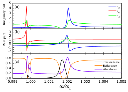
The effective permittivity and permeability of such a structure can be calculated by the extended Maxwell-Garnett theory [43, 44] which encompasses elements of the Mie theory within the formulae of the , . As such, the extended Maxwell-Garnett theory agrees very well with more rigorous approaches [8, 10, 11, 14, 15]. Figure 2a shows the real and imaginary parts of , , and for the above described system of metal-coated CuCl nanoparticles. One clearly observes a region of negative for . One can also identify a narrow frequency region around , where which is entirely within the region of negative . Within this region, and a NRI band occurs. Note that for the calculation of the the imaginary parts of , have been also taken into account by choosing the value of which possesses positive imaginary part (the structures under study are made from passive materials).
In order to verify the validity of the effective medium parameters depicted in figure 2a,b we have also employed the layer-multiple scattering method [34, 35, 36] (briefly outlined in section 2) in order to calculate the transmittance of light incident normally on a finite slab of an fcc crystal of the above nanospheres. We have chosen the fcc lattice since this type of lattice can satisfy a close-packed arrangement of spheres. The slab consists of 4 (001) fcc planes of nanospheres and the respective transmittance is shown in figure 2c. It is evident that within the NRI of figure 2b, the transmittance shows a maximum which is what one expects from a slab of NRI [3]. As light propagates through the slab, it is also attenuated due to the intrinsic losses of the constituent materials (CuCl and Drude-metal) as it is evident from the corresponding maximum of the absorbance curve of figure 2c within the NRI band. It is also evident that there is also a wider transmittance peak from to 1.002 which, however, corresponds to a region of refractive index with positive real part (the matching of these two frequency regions is not perfect as figure 2a is based on an effective medium approximation whilst figure 2b to an exact theory). In between these peaks as well as above the second peak, the transmittance is suppressed as only one of and becomes negative giving rise to a practically imaginary refractive index (see figures 2a,b).
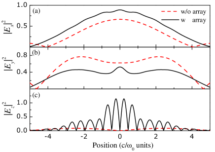
In order to probe the imaging properties of the above systems, we have applied the formalism developed in section 2 for the case of a single plane of metal-coated CuCl nanospheres. As a localized source of light we have considered a linear, infinitely thin, center-fed antenna of width , lying along the -axis. It is placed at a distance from the center of a single plane of spheres (see figure 1). Figure 3 shows the distribution of all three electric-field components along the line in the image plane (see figure 1), for frequency which corresponds to the low-frequency maximum of the transmittance curve of figure 2b. For comparison, we also show the corresponding curves in the absence of the plane of spheres. We note that the field distributions of all figures that follow contain both the far-field [ in equation (5)] and near-field [ in equation (5)] components. Since the chosen frequency () lies within the NRI band of the array of spheres (see above) we expect that the near-field components which are transmitted through the plane will be amplified. And this is indeed what we observe in figure 3. We observe that all three components components of the electric field are amplified with respect to the case where the plane of spheres is absent. This can occur only in the case of NRI where, as predicted by Pendry [3], both polarization modes are amplified when transmitted through a planar NRI slab. We remember that when only one of or occurs, the near-field amplification affects one of the polarization modes [25, 26, 27, 28, 29]. In addition to the near-field amplification of the electric field, we observe that the FWHM for the () and components () is considerably smaller than the free-space case suggesting a subwavelength imaging operation of the structure (see below). The -component (figure 3c) is much more amplified than the other two; however, the field distribution looks much more complicated, possibly, due to interference effects (the far-field is also included in the calculation) and the peculiarity of the source (the -component emitted by a center-fed antenna possesses a nodal line along the direction of the antenna axis).
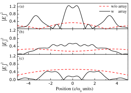
In order to confirm the fact that the near-field amplification shown in figure 3 is attributed to the occurrence of NRI, in figure 4 we show the same quantities, for the same calculation setup as in figure 3, but for frequency corresponding to the high-frequency transmission peak of figure 2b which lies out of the NRI band. We observe that only the -component (figure 4c) shows a similar trend as that of figure 3c. The -component is suppressed compared to the free-space case whilst the -component is barely amplified from the plane of nanospheres. Also, the subwavelength profile of the field distributions is lost as the maxima are almost as wide as those of the free-space case. So, judging from figure 4, we can infer that the field amplification for all polarizations and the subwavelength extension of the electric field of figure 3 are in accordance with the occurrence of NRI.
Next, in figure 5, we probe the imaging properties of thicker slabs, i.e., slabs containing more than one planes of nanospheres. We have chosen to depict the -component but similar effects are observed for the other two components. For the case of two planes of nanospheres (figure 5a), the field amplification is still evident although somewhat distorted at the center. There are also two satellite peaks evident which may influence a potential lensing application of the structure. For a 3-planes-thick slab (figure 5b) the amplification of the transmitted field is not as dramatic as for thinner slabs (Figs. 3a and 5a) whilst for the 4-planes-thick slab the amplification is evidently lost. At first glance, this seems to be an unexpected result: the extended Maxwell-Garnett theory [43, 44] which was employed for the calculation of in figure 2a refers to 3D collections of scatterers and it is is supposed to be more applicable to thick enough slabs. However, as both constituent materials of the nanospheres (metal and semiconductor) suffer from losses (especially the metal) we expect that thicker slabs mean longer optical paths for the transmitted field, and, therefore, higher losses which counterbalance the near-field amplification effect. This is also manifested in figure 2c where almost 90% of the incident power is absorbed within the slab (of 4 planes of spheres). Similar effects have been also measured experimentally for NRI metamaterials in the microwave regime [24].
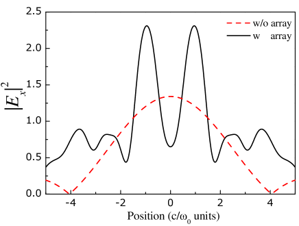
Finally, in order to study the image-resolution properties of the array of nanospheres, in figure 6, we have considered the case of two localized sources (small center-fed antennas) separated by a vertical subwavelength distance of . The array consists of a single plane of nanospheres since absorption is expected to deteriorate the image resolution for thicker slabs. The sources are placed symmetrically with respect to the center of a sphere, at a distance from the plane. As it is evident from the dashed curve of figure 6, the distance between the sources is too small to be resolved in free-space (a single peak appears). However, in the presence of the plane of nanospheres, the occurrence of NRI is accompanied by a dramatic increase in the image resolution which allows for distinguishing the two sources in space by use of visible light. We note that the image resolution can be further improved by using smaller nanospheres, down to radius of 15 nm. However, for CuCl spheres smaller than that, is no longer negative [45] around the exciton resonance and a NRI band is not expected to occur.
4 Conclusion
It has been shown that arrays of metal-coated semiconductor nanospheres can exhibit NRI around the exciton resonance (if such exists) of the semiconductor. The existence of NRI has been studied by use of the extended Maxwell-Garnett theory and confirmed by rigorous EM calculations of light transmittance. Within the NRI band, an array of such spheres can amplify the near-field for both polarization modes, in accordance with Pendry’s theory [3]. The near-field amplification is accompanied by subwavelength image resolution that is only limited by the inherent losses of the metal and the semiconductor. The systems studied in this work are strong candidates for NRI metamaterials in the optical regime due to their fabrication with existing methods of colloidal chemistry [40, 41, 42, 46].
References
References
- [1] Lakhtakia A and Mackay T G 2007 Opt. Photonics News 18 32
- [2] Veselago V G 1968 Sov. Phys.-Usp. 10 509
- [3] Pendry J B 2000 Phys. Rev. Lett. 85 3966
- [4] Negative-Refraction Metamaterials, edited by G. V. Eleftheriades and K. G. Balmain (Wiley, New Jersey, 2005).
- [5] O’Brien S and Pendry J B 2002 J. Phys.: Condens. Matter14 4035
- [6] Holloway C L, Kuester E F, Baker-Jarvis J and P. Kabos 2003 IEEE Trans. Antennas Propag. 51 2596
- [7] Huang K C, Povinelli M L and Joannopoulos J D 2004 Appl. Phys. Lett. 85 543
- [8] Yannopapas V and Moroz A 2005 J. Phys.: Condens. Matter17 3717
- [9] Felbacq D and Bouchittè G 2005 New J. Phys.7 159
- [10] Wheeler M S, Aitchison J S and Mojahedi M 2005 Phys. Rev.B 72 193103
- [11] Wheeler M S, Aitchison J S and Mojahedi M 2005 Phys. Rev.B 73 045105
- [12] Jylhä L, Kolmakov I, Maslovski S and Tretyakov S 2006 J. Appl. Phys. 99 043102
- [13] MacKay T G and Lakhtakia A 2006 J. Appl. Phys.100 063533
- [14] Yannopapas V and Vitanov N V 2006 Phys. Rev.B 74 193304
- [15] Yannopapas V 2007 Phys. Rev.B 75 035112
- [16] Rockstuhl C, Lederer F, Etrich C, Pertsch T and Scharf T 2007 Phys. Rev. Lett. 99 017401
- [17] Peng L, Ran L, Chen H, Zhang H, Kong J A and Grzegorczyk T M 2007 Phys. Rev. Lett. 98 157403
- [18] Schuller J A, Zia R, Taubner T and Brongersma M L 2007 Phys. Rev. Lett. 99 107401
- [19] Redl F X, Cho K- S, Murray C B and O’Brien S 2003 Nature (London) 423 968; Saunders A E and Korgel B A 2005 ChemPhysChem 6 61; Shevchenko E V, Talapin D V, Kotov N A, O’Brien S and Murray C B 2006 Nature (London) 439 55; Kalsin A M, Fialkowski M, Paszewski M, Smoukov S K, Bishop K J M and Grzybowski B A 2006 Science 312 420
- [20] Parazzoli C G, Greegor R B, Li K, Koltenbah B E C and Tanielian M 2003 Phys. Rev. Lett. 90 107401
- [21] Houck A A, Brock J B and Chuang I L 2003 Phys. Rev. Lett. 90 137401
- [22] Lagarkov A N and Kissel V N 2004 Phys. Rev. Lett. 92 077401
- [23] Grbic A and Eleftheriades G 2004 Phys. Rev. Lett. 92 117403
- [24] Aydin K, Bulu I and Ozbay E 2007 Appl. Phys. Lett. 90 254102; Ozbay E and Aydin K 2007 Photon. Nanostruct.- Fundam. Applic., doi:10.1016/j.photonics.2007.09.003
- [25] Wiltshire M C K, Pendry J B, Young I R, Larkman D J, Gilderdale D J and Hajnal J V 2001 Science 291 849
- [26] Wiltshire M C K, Pendry J B, and Hajnal J V 2006 J. Phys.: Condens. Matter18 L315
- [27] Ono A, Kato J and Kawata S 2005 Phys. Rev. Lett. 95 267407
- [28] Fedorov G, Maslovski S I, Dorofeenko A V, Vinogradov A P, Ryzhikov I A and Tretyakov S A 2006 Phys. Rev.B 73 035409
- [29] Alitalo P, Simovski C, Viitanen A and Tretyakov S 2006 Phys. Rev.B 74 235425
- [30] Yannopapas V 2007 Phys. Stat. Sol. (RRL) 1 208
- [31] Jackson J D 1975 Classical Electrodynamics (Wiley: New York)
- [32] Naus H W L 2007 Phys. Rev.E 76 026602
- [33] Modinos A, Yannopapas V and Stefanou N 2000 Phys. Rev.B 61 8099
- [34] Stefanou N, Karathanos V and Modinos A 1992 J. Phys.: Condens. Matter4 7389
- [35] Stefanou N, Yannopapas V and Modinos A 1998 Comput. Phys. Commun. 113 49
- [36] Stefanou N, Yannopapas V and Modinos A 2000 Comput. Phys. Commun. 132 189
- [37] Gantzounis G and Stefanou N Phys. Rev.B 73 035115
- [38] Abramowitz M and Stegun I A 1965 Handbook of Mathematical Functions (Dover: New York)
- [39] Artoni M, La Rocca G and Bassani F 2005 Phys. Rev.E 72 046604
- [40] Orel Z C, Matijević E and Goia D V 2003 Colloid. Polym. Sci. 281 754
- [41] Fukumi K, Chayahara A, Kageyama H, Kadono K, Akai T, Kitamura N, Mizoguchi H, Horino Y, Makihara M, Fujii K, Hayakawa J 1999 J. Non-Cryst. Sol. 259 93
- [42] Cozzoli P D, Pellegrino T and Manna L 2006 Chem. Soc. Rev. 35 1195
- [43] Doyle W T 1989 Phys. Rev.B 39 9852
- [44] Ruppin R 2000 Opt. Commun. 182 273
- [45] Yannopapas V 2007 Appl. Phys. A 87 259
- [46] Gaponenko S V, Germanenko I N, Gribkovskii V P, Zimin L G, Lebed V Y and Malinovskii I E 1993 Physica B 185 588
