Tunable Plasmon Molecules in Overlapping Nanovoids
Abstract
Coupled and shape-tailored metallic nanoparticles are known to exhibit hybridized plasmon resonances. This Letter discuss the optical properties of a complementary system formed by overlapped nanovoid dimers buried in gold and filled with silica. This is an alternative route for plasmon engineering that benefits from vanishing radiation losses. Our analysis demonstrates the possibility of designing artificial plasmon molecules on the basis of void plasmon hybridization, which allows fine mode tuning by varying the overlap between voids. The proposed structures could find application to both signal processing through buried optical elements and tunable-plasmon biosensing.
pacs:
73.20.Mf,78.67.-n,84.40.AzPlasmons in metallic particles have recently attracted considerable attention as promising candidates to realize photonic devices, enabling manipulation of light over sub-micron distances. The frequency of plasmon resonances can be tuned at will by nanoengineering the particle environment and playing with different geometries Prodan et al. (2003); Teperik et al. (2004); Aizpurua et al. (2003); Teperik et al. (2005); Nordlander et al. (2004); Burda et al. (2005); Romero et al. (2006); Sánchez-Iglesias et al. (2006). The suite of available nontrivial structures includes nanoshells Prodan et al. (2003); Teperik et al. (2004), nanorings Aizpurua et al. (2003), nanovoids Teperik et al. (2005), nanorods Burda et al. (2005), and exotic polyhedral crystallites Sánchez-Iglesias et al. (2006). Plasmon hybridization originating in intra- Prodan et al. (2003) and inter-particle Nordlander et al. (2004) interactions adds up an extra handle to fine tuning resonant mode energies, particularly in dimers near the touching limit Romero et al. (2006); Danckwerts and Novotny (2007).
In this context, the guiding properties of nanoparticle linear arrays have been thoroughly investigated with a view to designing optical interconnects based upon plasmon hopping between particles Weeber et al. (2001); Maier et al. (2003). However, plasmon propagation in these systems is found to be severely damaged by both dissipation in the metal and radiative losses. The latter are minimized by relying on small particles ( nm), but there is a tradeoff between both types of losses. Ultimately, absorption limits propagation to sub-micron distances in small particles Maier et al. (2003). This problem can be solved by using instead larger voids or dielectric inclusions buried in metal. Actually, the radiative damping of hybridized void-like plasmons in nanoshells decreases extremely rapidly with increasing shell thickness Teperik et al. (2004). The basic unit of such void arrays is the void dimer, to which we devote this work.
In the electrostatic limit, the mode frequencies of the particle array and its complementary void array are interconnected through the general, exact relation García de Abajo and Aizpurua (1997), where and are the permittivities of the material inside and outside the spherical boundaries, respectively, and are eigenvalues that depend exclusively on geometry and not on the actual dielectric properties of the materials involved. When the media under consideration are air and a Drude metal described by
| (1) |
one obtains the sum rule Apell et al. (1996). Therefore, the analysis of electrostatic void arrays is fully contained in the electrostatic particle array. We will however consider relatively large voids yielding longer propagation distances. Then, retardation effects become dominant for sizes above the skin depth ( nm at visible and NIR frequencies), and therefore a separate analysis becomes necessary.
In this work, we describe the optical properties of plasmon molecules formed in overlapping nanovoids buried in metal. Similar to particle dimers Nordlander et al. (2004), large shifts of hybridized modes are observed, controlled by varying the degree of overlap, while significant field enhancement takes place near the junction region. But unlike particle dimers, void dimers do not present a singular transition near touching conditions. More precisely, the unphysical mode observed in the separate particle dimer Romero et al. (2006), characterized by a net induced charge sitting in each particle, becomes now physical for the voids, although the inter-void interaction is drastically reduced in non-overlapping systems due to the skin-depth effect.
We rigorously solve Maxwell’s equations in the frequency domain for overlapping void dimers filled with silica using the boundary element method (BEM) García de Abajo and Howie (1998), in which surface charges and currents are introduced to match the fields across dielectric boundaries, thus resulting in a set of surface-integral equations that is transformed in turn into a linear-algebra problem upon discretization of the integrals. The NIR permittivity of gold is modeled for simplicity through Eq. (1) with parameters eV and eV Kreiter et al. (2002), while we take for silica.
Fully buried voids are unaccessible to external radiation, so light scattering cannot be employed to characterize them. Instead, we investigate the photonic local density of states (LDOS) in the silica region, defined as the combined local intensity of all eigenmodes of the system under consideration Fussell et al. (2004). With this definition, the LDOS projected along the direction of an atomic-decay transition-dipole is related to the decay rate as . In practical terms, the LDOS can be calculated from the field scattered by the void boundaries, projected along the dipole, according to
where the first term on the right hand side is the silica LDOS. Here, we consider projection directions parallel and perpendicular to the dimer axis and give the LDOS normalized to its value in silica.


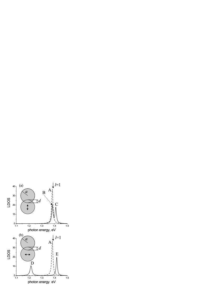
We show in Fig. 1 the LDOS at the center of one of the silica-filled voids of a dimer formed by spheres of radius nm with d=60 nm overlap (solid curves). For comparison, the isolated-void LDOS is also represented (dashed curves), exhibiting a prominent feature corresponding to the electric Mie resonance in agreement with the analytical expression (see arrows) Weinstein (1969)
| (2) |
where , and are spherical Bessel and Hankel functions, and is the orbital momentum number. The small mismatch between BEM calculations and the analytical mode frequency originates in non-resonant contributions to the dipole-induced field of the former.
The -plasmon mode of the single void is degenerate, and one can expect partial lifting of this degeneracy due to void overlap. This is clearly observed in Fig. 1. The resulting modes have and azimuthal symmetry in Figs. 1(a) and (b), corresponding to transition dipoles oriented parallel and perpendicular to the dimer axis, respectively. The latter is doubly degenerate, so that the overall number of 6 modes is preserved after inter-void interaction is switched on. The dimer modes are hybridized and energy split, but the splitting is significantly larger for the transverse low-energy feature D. The origin of this can be traced back to strong interaction within the inter-void opening, which is made possible for co-directional transverse orientations of the exciting dipoles and has similar nature as gap modes in particle dimers Nordlander et al. (2004). In a related context, this gives rise to rim modes localized at the opening of voids partly buried in flat metal surfaces Cole et al. (2007).
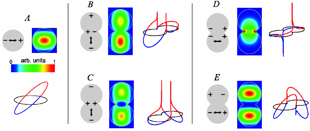
This intuition is supported by the induced-field distributions shown in Fig. 2 for features A-E of Fig. 1. See for instance the large increase in field intensity near the void junction region associated to peak D. This is accompanied by significant piling up of induced charge, as shown in the graph to the right of the contour plot. However, peak E has vanishing intensity in the voids opening due its quadrupolar symmetry, and therefore it suffers a rather moderate shift.
These results suggest the possibility to design plasmon molecules of tailored frequency and symmetry. For example, a quadrupole plasmon mode can be obtained in the dimer near the single-void dipole mode frequency (E in Figs. 1 and 2). More sophisticated plasmon modes should also be possible by combining several voids, with the dimer acting as a building block.
In contrast to metallic-particle dimers, in which plasmons interact through a dielectric environment Romero et al. (2006), our void plasmons are coupled only through the region of overlap. Therefore, plasmon mixing critically depends on the overlap distance and can be significantly reduced in buried geometries, thus simplifying the understanding of the resulting plasmon molecule. In particular, modes B, C, and E are reliably described in terms of dipole-dipole interaction, whereas mode D, which lies further away from the single-void dipole resonance, is dominated by the rim-like mode, involving a large degree of mixing of higher-order modes.
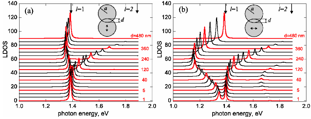
The full dependence of the void dimers is presented in Fig. 3. Several characteristic features are clearly resolved in the evolution of the plasmon modes:
(i) Mode splitting is consistently larger for the transverse orientation of the dipole, in good agreement with the conclusions extracted from Figs. 1 and 2.
(ii) As anticipated above, the interaction between voids switches on smoothly between non-touching and overlapping configurations, in contrast to the singular transition observed for particle dimers Romero et al. (2006).
(iii) The low-energy dipole modes evolve smoothly towards the single-void dipole when the overlap is complete (). An initial red shift after touching is followed by a blue shift as increases. In the rim-like mode [see D in Figs. 1 and 2, and low-frequency features in Fig. 3(c)], a maximum red shift is produced at an optimum distance resulting from the compromise between increasing mode volume as becomes smaller (this lowers the kinetic energy of the mode) and increasing inter-void interaction as increases (this lowers the mode energy due to inter-mode attraction).
(iv) The high-energy quadrupolar modes march towards the single-void quadrupole as increases and the quadrupole-mode LDOS becomes zero at the center of a single-void.
(v) A weak transition resonance is observed in the vicinity of 1.7 eV [Fig. 3(b)], originating in higher-order void multipoles that are the counterpart of the left-most rim-like mode.
The plasmon widths determine how well the modes are defined. In this sense, the 1.7 eV resonance just noted is a well-defined one. In fact, the width of all our reported plasmons arise from metal absorption, so that modes associated to fields mainly contained in the silica and characterized by minimum overlap with the metal will have longer lifetimes. This is clear when comparing modes D and E in Figs. 1(b) and 2: D is broader because it has larger intensity in the metal (see region near the void junction). However, much of the field intensity lies in the silica, and that is why the mode widths are considerably smaller than in Eq. (1).
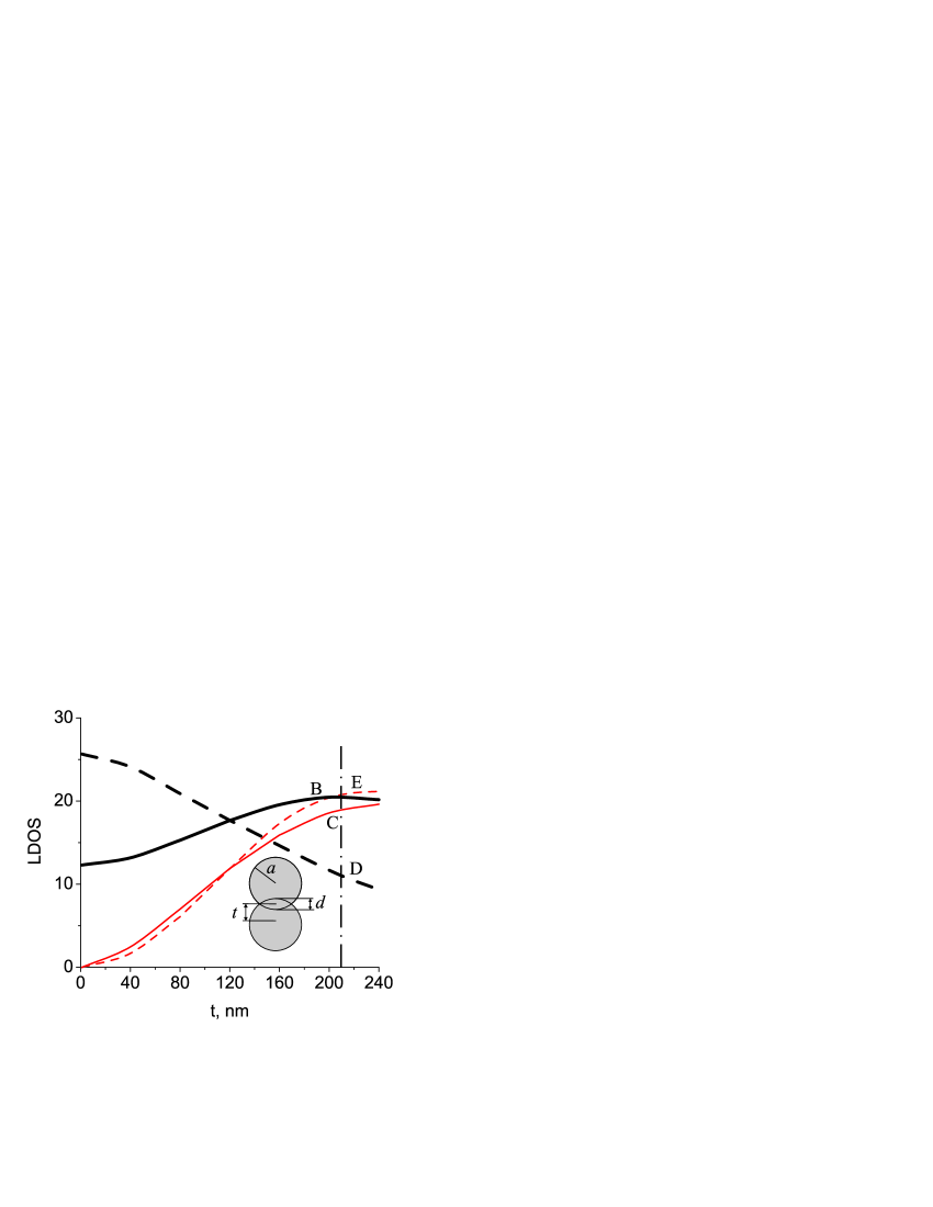
Finally, the location of the probing dipole determines the actual degree of coupling to the plasmons. This is illustrated in Fig. 4, which shows the evolution of the plasmon LDOS along the dimer axis for features B-E of Fig. 1. Interestingly, only the low-energy hybrid plasmons (B and D), which have the original dipole symmetry, contribute to the LDOS at the dimer center (thick curves). The high-energy modes have an overall quadrupolar character and can only be excited by dipoles displaced with respect to the dimer central region.
In summary, we have investigated the optical properties of two overlapping silica inclusions embedded in gold and found hybridized plasmon modes, the mixing of which can be effectively controlled by changing the degree of geometrical overlap. This opens up the possibility to realize radiative-free plasmon molecules through dielectric inclusions buried in metal. Large field enhancements are observed on resonance near the overlap region, which can find application to surface-enhanced Raman spectroscopy and other forms of biosensing. The void dimer constitutes the basic building block of buried optical circuits for future on-chip interconnects and switching elements. In contrast to particle arrays, void arrays will benefit from minimum cross-talk across the metal and vanishing radiative losses, thus allowing a step forward in nanoscale integration.
This work has been supported in part by the Spanish MEC (NAN2004-08843-C05-05) and by the EU (NMP3-CT-2004-500252 and STRP-016881-SPANS). T.V.T. acknowledges support from the Russian Academy of Sciences, Russian Foundation for Basic Research (Grants 05-02-17513, 07-02-91011, and 06-02-81007).
References
- Prodan et al. (2003) E. Prodan, C. Radloff, N. J. Halas, and P. Nordlander, Science 302, 419 (2003).
- Teperik et al. (2004) T. V. Teperik, V. V. Popov, and F. J. García de Abajo, Phys. Rev. B 69, 155402 (2004).
- Aizpurua et al. (2003) J. Aizpurua, P. Hanarp, D. S. Sutherland, M. Käll, G. W. Bryant, and F. J. García de Abajo, Phys. Rev. Lett. 90, 057401 (2003).
- Teperik et al. (2005) T. V. Teperik, V. V. Popov, and F. J. García de Abajo, Phys. Rev. B 71, 085408 (2005).
- Nordlander et al. (2004) P. Nordlander, C. Oubre, E. Prodan, K. Li, and M. I. Stockman, Nano Lett. 4, 899 (2004).
- Burda et al. (2005) C. Burda, X. Chen, R. Narayanan, and M. A. El-Sayed, Chem. Rev. 105, 1025 (2005).
- Romero et al. (2006) I. Romero, J. Aizpurua, G. W. Bryant, and F. J. García de Abajo, Opt. Express 14, 9988 (2006).
- Sánchez-Iglesias et al. (2006) A. Sánchez-Iglesias, I. Pastoriza-Santos, J. Pérez-Juste, B. Rodríguez-González, F. J. García de Abajo, and L. Liz-Marzán, Adv. Mater. 18, 2529 (2006).
- Danckwerts and Novotny (2007) M. Danckwerts and L. Novotny, Phys. Rev. Lett. 98, 026104 (2007).
- Weeber et al. (2001) J. C. Weeber, J. R. Krenn, A. Dereux, B. Lamprecht, Y. Lacroute, and J. P. Goudonnet, Phys. Rev. B 64, 045411 (2001).
- Maier et al. (2003) S. A. Maier, P. G. Kik, H. A. Atwater, S. Meltzer, E. Harel, B. E. Koel, and A. A. G. Requicha, Nat. Mater. 2, 229 (2003).
- García de Abajo and Aizpurua (1997) F. J. García de Abajo and J. Aizpurua, Phys. Rev. B 56, 15873 (1997).
- Apell et al. (1996) S. P. Apell, P. M. Echenique, and R. H. Ritchie, Ultramicroscopy 65, 53 (1996).
- García de Abajo and Howie (1998) F. J. García de Abajo and A. Howie, Phys. Rev. Lett. 80, 5180 (1998); Phys. Rev. B 65, 115418 (2002).
- Kreiter et al. (2002) M. Kreiter, S. Mittler, W. Knoll, and J. R. Sambles, Phys. Rev. B 65, 125415 (2002).
- Fussell et al. (2004) D. P. Fussell, R. C. McPhedran, and C. Martijn de Sterke, Phys. Rev. E 70, 066608 (2004).
- Weinstein (1969) L. A. Weinstein, Open Resonators and Open Waveguides (Golem, New York, 1969).
- Cole et al. (2007) R. M. Cole, J. J. Baumberg, F. J. García de Abajo, S. Mahajan, M. Abdelsalam, and P. N. Barlett, Nano Lett. 7, 2094 (2007).