l
Fabry-Perot interference, Kondo effect and Coulomb blockade in carbon nanotubes
Abstract
High quality single wall carbon nanotube quantum dots have been made showing both metallic and semiconducting behavior. Some of the devices are identified as small band gap semiconducting nanotubes with relatively high broad conductance oscillations for hole transport through the valence band and low conductance Coulomb blockade oscillations for electron transport through the conduction band. The transition between these regimes illustrates that transport evolves from being wave-like transmission known as Fabry-Perot interference to single particle-like tunneling of electrons or holes. In the intermediate regime four Coulomb blockade peaks appear in each Fabry-Perot resonance, which is interpreted as entering the SU(4) Kondo regime. A bias shift of opposite polarity for the Kondo resonances for one electron and one hole in a shell is in some cases observed.
I Introduction
Single wall carbon nanotubes (SWCNT) are interesting objects for the study of low dimensional mesoscopic systems, where the observed phenomena crucially depends on the coupling to the contacts. For good contact, the SWCNT acts as an electron wave guide creating resonances at certain energies. Such systems are regarded as open quantum dots with the resonances corresponding to the broad energy levels of the quantum dot Liang et al. (2001). In the opposite limit of very low transparency, the electrons are forced to tunnel one by one due to Coulomb blockade and the energy levels sharpens due to their longer life time Tans et al. (1998a); Bockrath et al. (1997). In this so-called closed quantum dot regime the electron number on the SWCNT is well-defined except at charge-degeneracy points where single electron tunneling occurs. An intermediate regime also exists in which the electron number on the dot is still fixed but significant cotunneling is allowed. This leads to different kinds of Kondo effects related to the total excess spin Goldhaber-Gordon et al. (1998); Nygård et al. (2000); Paaske et al. (2006) and/or the orbital degree of freedom on the SWCNT quantum dot Jarillo-Herrero et al. (2005); Makarovski et al. (2006). We will in this paper examine the transition between these regimes in small band gap semiconducting nanotubes, where the coupling to the SWCNT is different for transport through the valence and conduction band Cao et al. (2005a). High quality measurement is presented from each transparency regime showing that each Fabry-Perot oscillation develops into four Coulomb blockade resonances with finite conductance in the valleys for intermediate transparency (Kondo effect) and well known Coulomb diamond patterns with four-fold degenerate shell structure at lowest transparency Sapmaz et al. (2005).
II Experimental methods
SWCNTs are grown from predefined catalyst islands by chemical vapor deposition on a highly doped silicon substrate capped by a 500 nm silicon dioxide layer. After growth, pairs of electrodes are defined by electron beam lithography some microns away from the catalyst islands in hope that one SWCNT bridges the gap between the two electrodes. In the case of the small band gap semiconducting SWCNT the electrodes consist of Au/Pd bilayers (40 nm/10 nm). Finally bonding pads of Au/Cr are made by optical lithography connecting the electron beam lithography defined electrodes. The devices are electrically probed at room temperature with typical resistances in the range of 20-200 k. These are cooled to low temperatures where device characteristics clearly reveals if only one SWCNT is in the gap. More details on device fabrication can be found in Refs. Grove-Rasmussen et al. (2007); Jørgensen et al. (2006). The measurements presented in this article are mostly made at 4 K in a DC-setup.
III Metallic and Semiconducting nanotubes
SWCNTs have the remarkable property that depending on the exact arrangement of the carbon atoms they can either be metals or semiconductors. Figure 1 shows the gate (and temperature) dependence of the linear conductance for two different types of SWCNTs, which defines whether the nanotube is semiconducting or metallic. Figure 1(a) displays the behavior of a metallic SWCNT characterized by its relatively constant linear conductance as a function of gate voltage close to room temperature. On the contrary the behavior shown in Fig. 1(b) corresponds to a semiconducting SWCNT due to its strongly gate dependent linear conductance Tans et al. (1998b). The semiconducting SWCNT has clearly high conductance for negative gate voltages, which is due to hole transport through the valence band as indicated in the inset showing the band structure (p-type). In the range of 4 V V the chemical potential of the leads is aligned with the band gap, i.e., no conduction occurs. At higher temperatures signs of electron transport through the conduction band is seen at high positive gate voltages due to thermal excitation of electrons into the conduction band. The SWCNT shown in Fig. 1(b) has a relative large band gap, while conduction for small band gap semiconductors reappears for positive gate voltage in the gate range shown due to electron transport through the conduction band (see below). Note, that the resistance between the two devices differ by an order of magnitude due to different coupling to the leads. In general the coupling can to some extent be controlled by choice of electrode material Babić et al. (2004a).
Figure 1(a-b) also shows the temperature dependence, where the gate dependence of the linear conductance for both devices evolves into regular oscillations at low temperature. These oscillations are a manifestation of Coulomb blockade, which as mentioned above happens for SWCNT weakly coupled to the leads. The regularity of the Coulomb oscillations indicates whether good quality of the SWCNT has been obtained or if more than one SWCNT is bridging the gap between the electrodes. For high quality SWCNTs regular oscillations should persist through a gate region of typically V as shown in (a). On the contrary if the SWCNT has defects only small regions of gate voltage might have well behaved oscillations.

IV Small band gap semiconducting nanotubes
We will now focus on small band gap semiconducting SWCNTs, where the band gap is so small that transport can be tuned from hole transport through the valence band to electron transport through the conduction band by the back gate Jarillo-Herrero et al. (2004); Cao et al. (2005b, 2004, a).

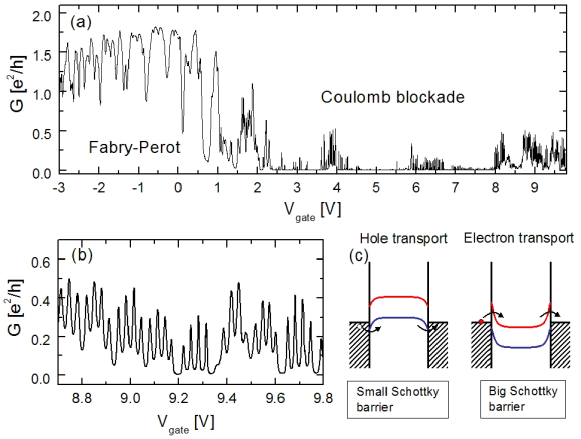
Figure 2(a) shows the linear conductance versus gate voltage at source-drain voltages mV for a small band gap SWCNT at K (device 1). The nature of the SWCNT is identified by the relatively high conductance region for negative gate voltages (hole transport) in contrast to the low conductance region for positive gate voltages (electron transport). The broad oscillations for hole transport for gate voltages between V and 0.5 V are a manifestation of the Fabry-Perot interference pattern, i.e., an open quantum dot Liang et al. (2001). In contrast for positive gate voltages regular low conductance oscillations are observed due to Coulomb blockade. Figure 2(b) shows the high positive gate region for electron transport where relatively high conductance Coulomb blockade resonances are seen. They are spaced into four reflecting the spin and orbital degree of freedom. When this device is cooled to lower temperature (50 mK) Kondo resonances are seen within the four-fold shell structure (not shown) in contrast to the lower conducting region, e.g., gate voltages from 5 V to 8 V, where only single electron tunneling is possible.
The different transparency of the n- and p-type regions can be understood from Fig. 2(c). For negative gate-voltages (left figure) the bands are bending in such a way that holes can tunnel from source into the valence band and out to drain. The Schottky barrier for hole transport is relatively small because the workfunction of the Pd contacts is close to the valence band edge leading to a relatively high conductance Cao et al. (2005a). Transport can be changed to electron transport through the conduction band (right figure) by applying positive voltage to the gate. The Schottky barrier is in this case significantly larger leading to a low coupling of the SWCNT to the electrodes. Between these two transport regions no transport is allowed because the chemical potential in the leads is within the band gap of the semiconducting SWCNT.

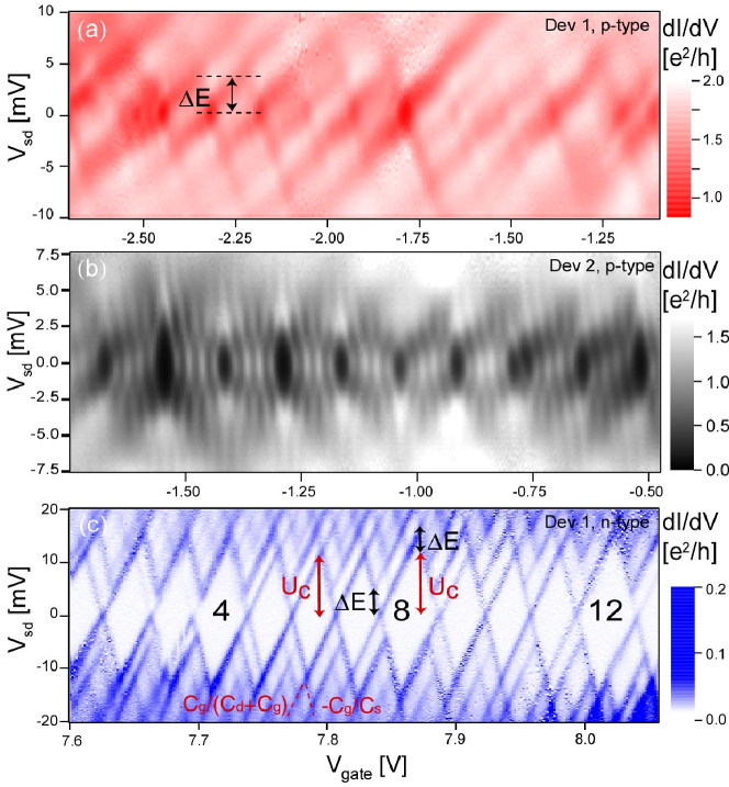
More information on the transport properties can be revealed by bias spectroscopy, where the differential conductance is measured as a function of gate and bias voltages. A bias spectroscopy plot of part of the Fabry-Perot region is shown in Fig. 3(a). The low conductance regions (red areas) form a mesh due to interference of the hole waves reflected back and forth. Regarding the device as a quantum dot the white regions at zero bias correspond to being in resonance, while a red regions are off resonance. The level spacing can be extracted as indicated in Fig. 3(b) by the black arrow mV consistent with the device being around nm. Here we have used a linear dispersion since we are far from the band gap. Furthermore, a four-fold degeneracy of the level is assumed, which is clearly revealed in the n-type region of the device (see below). The device has a high asymmetric resistive coupling, because the conductance at resonance is lower than . The asymmetry can be found from , where is the conductance at resonance yielding . The capacitive couplings to the source and the drain electrodes are also slightly different or/and the capacitive coupling to the gate is comparable to the source and drain capacitance because of the different slopes of the low conductance lines (red). The capacitances will be examined more closely in the Coulomb blockade case below.
Figure 3(b) shows a bias spectroscopy plot in the p-type region for another small band gap semiconducting SWCNT with lower transparency (device 2). Signs of Fabry-Perot oscillations are still observed, but each Fabry-Perot resonance is split into four smaller peaks Cao et al. (2005a). These peaks are due to Coulomb blockade and single hole tunneling, i.e., the four-fold degenerate level becomes visible due to quantization of the charge. The finite conductance in the valleys between the peaks are indication of SU(4) Kondo effect, which will be treated in more detail below Jarillo-Herrero et al. (2005).
Figure 3(c) shows a bias spectroscopy plot in the n-type region of device 1, where the transparency is reduced even further. Clear Coulomb blockade diamonds and excited states are observed. The numbers indicate the relative electron filling of the SWCNT quantum dot and a number dividable by four corresponds to a filled shell identified as three small diamonds followed by a bigger diamond. A shell thus consists of a four-fold degenerate level as expected due to orbital and spin degrees of freedom. The charging energy can be extracted from the three small diamonds as half the source-drain height mV (left red arrow). The orbital splitting and exchange energy are very small since the three consecutive small diamonds in one shell are almost equal in height, e.g., diamonds 5, 6 and 7. Every fourth diamond is bigger (filled shell) since the addition of the first electron in a new shell requires both a charging energy and a level spacing energy. The additional diamond height of the larger diamonds thus yields the level spacing mV (right black arrow). This is consistent with the level spacing identified from the excited state lines shown for electron filling 7 (left black arrow). The asymmetry of the diamonds are due to the capacitive coupling of the source , drain and gate electrodes to the SWCNT. Estimating the slopes and of the two lines constituting the diamond (dashed red lines) as well as the gate voltage distance mV between two Coulomb diamonds (diamond 7) the capacitances can be found. We find aF, aF and aF by , and , where is the total capacitance to the surroundings, corresponds to aligning the electrochemical potentials of the dot with the source/drain and an asymmetric biasing with the drain on ground is used Hanson et al. (2006). The equal magnitude of the gate and source/drain capacitive coupling thus makes the diamond asymmetric.

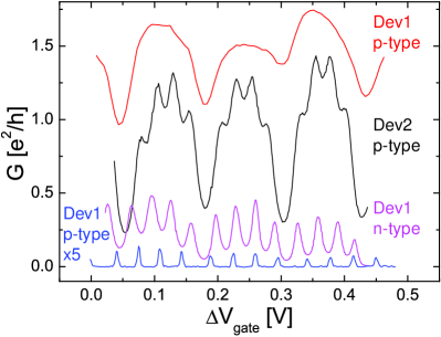
The transition between the different transparency regimes is even more clearly revealed in the linear conductance versus gate voltage shown in Fig. 4. All curves are extracted at zero bias from bias spectroscopy plots in the p- or n-type region of the two small band gap semiconducting SWCNTs presented above (device 1 and 2). The most conducting device (red curve) shows broad Fabry-Perot oscillations with no sign of single hole transport consistent with holes added continuously to the SWCNT due to the relatively good coupling. When the coupling to the SWCNT weakens, the holes become more localized on the SWCNT and single hole transport is observed (black curve). Four Coulomb blockade resonances emerge in each broad Fabry-Perot resonance consistent with each resonance (level) being four-fold degenerate. For even weaker coupling a closed quantum dot is formed (magenta and blue curves), where the measurement stems from the n-type region of device 1. The curves are not scaled but only shifted along the gate axis. Similar observations have been made by Cao et al. on very clean suspended small band gap semiconducting SWCNTs and also in our measurement the Coulomb energy seem to diminish as the transparency increases Cao et al. (2005a). This is seen by the distance between the peaks within one shell for the magenta curve is smaller than in the case of the black curve.
IV.1 Intermediate regime
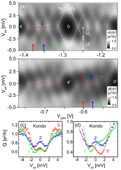
We now want to examine the transport behavior in the regime of intermediate transparency in more detail. Figure 5(a) shows a bias spectroscopy plot taken from Fig. 3(b) with the filling of only two shells each containing a four-fold degenerate level, i.e., addition of 8 holes as the gate voltage becomes more negative. The numbers 0,..,4 show the number of holes in one of the shells. The Coulomb diamonds are still faintly visible despite the relative high transparency, where the big diamond(s) correspond to filled shells. The charging energy and level spacing can be estimated as above yielding meV (see arrows). Similarly, to the case of the closed quantum dot we deduce the capacitances of the device from the slopes of the diamond sides () and the voltage distance between two consecutive Coulomb blockade resonances ( mV) in the shell giving aF, aF and aF. In the case of the closed quantum dot of device 1, the gate capacitance is almost identical ( aF) consistent with the two devices having the same geometry. In contrast to the more closed dot (device 1), the source and drain capacitances are increased. We speculate that increasing the transparency to the source and drain contacts leads to an increase of the source and drain capacitances because the wave function extends below the contact. Such behavior is also consistent with the charging energy diminishing with increasing transparency as noted above. Figure 5(c) shows the bias cuts in the center of the diamonds for filling 1, 2 and 3 (see colored arrows), where clear zero bias peaks are present. These zero bias peak are manifestation of the SU(4) Kondo effect due to the four-fold degeneracy of the shell Jarillo-Herrero et al. (2005); Choi et al. (2005). The FWHM of the Kondo peak for filling of 2 holes yields 1.5 mV by a Lorentzian fit corresponding to a Kondo temperature of 5.1 K higher than the measurement temperature of 4K. The center positions of the Kondo and Coulomb blockade resonances within a shell are at zero bias as expected indicated by the red dashed line.
Figure 5(b) shows another gate region from Fig. 3(b) with SU(4) Kondo effect showing a different behavior of the Coulomb blockade and Kondo resonance positions. The Coulomb blockade resonances are clearly shifted to more negative source-drain voltage as the holes are added to the shell with a slope of (red dashed line). Furthermore, the Coulomb blockade resonances for the hole transitions 0’-1’ (1’-2’) and 3’-4’ (2’-3’) are shifted equally in bias but with different polarity. Similarly, the Kondo peak for holes fillings 1’ and 3’ (i.e., one electron) are shifted oppositely in bias ( meV) as shown in Fig. 5(d), while the Kondo peak for hole filling 2’ is centered at zero bias. We note that an opposite slope is also found in Fig. 3(b) ( V). This behavior has previously been observed in carbon nanotubes showing four-fold shell structure Makarovski et al. (2006); Babić et al. (2004b) and also for spin half Kondo effect in a GaAs based quantum dot Simmel et al. (1999). In Ref. Makarovski et al. (2006) the authors speculate that it is related to SU(4) Kondo effect, because SU(4) theory predicts a shifted density of states compared to the spin half Kondo effect for electron filling 1 in equilibrium Lim et al. (2006). However, in Ref. Babić et al. (2004b); Simmel et al. (1999) and theoretical work on spin half Kondo effect Krawiec and Wysokiński (2002) the behavior was attributed to the asymmetry of the coupling to the leads, which shifts the Kondo peaks to finite biases. The asymmetry can be extract from the linear conductance of the Kondo resonance in the unitary limit or from current plateau corresponding to the total current through one level Babić et al. (2004b). However, at this temperature the Kondo resonances are not saturated and the current plateaus are too smeared to extract the couplings. More experimental work at lower temperature as well as precise theoretical predictions of these shifts are needed to elaborate more on this effect.

V Conclusion
In conclusion measurements on very clean single wall carbon nanotube quantum dots have been presented. We focused on small band gap semiconducting SWCNTs and the transition from an open to a closed quantum dot (Fabry-Perot interference to Coulomb blockade). The appearance of four peaks is observed in each Fabry-Perot resonance as the transparency is decreased, which is interpreted as entering the SU(4) Kondo regime. The Kondo resonances for one hole and one electron in a shell are in some cases shifted to opposite biases. At even lower transparency clear Coulomb blockade shell structure with a four-fold degeneracy due to orbital and spin degrees of freedom is observed.
VI Acknowlegdement
We would like to thank Jens Paaske for discussions and the support of the EU-STREP Ultra-1D program.
References
- Liang et al. (2001) W. Liang, M. Bockrath, D. Bozovic, J. H. Hafner, M. Tinkham, and H. Park, Nature 411, 665 (2001).
- Tans et al. (1998a) S. J. Tans, M. H. Devoret, R. J. A. Groeneveld, and C. Dekker, Nature 394, 761 (1998a).
- Bockrath et al. (1997) M. Bockrath, D. Cobden, P. McEuen, N. Chopra, A. Zettl, A. Thess, and R. Smalley, Science 275, 1922 (1997).
- Goldhaber-Gordon et al. (1998) D. Goldhaber-Gordon, H. Shtrikman, D. Mahalu, D. Abusch-Magder, U. Meirav, and M. A. Kastner, Nature 391, 156 (1998).
- Nygård et al. (2000) J. Nygård, D. H. Cobden, and P. E. Lindelof, Nature 408, 342 (2000).
- Paaske et al. (2006) J. Paaske, A. Rosch, P. Wolfle, N. Mason, C. M. Marcus, and J. Nygård, Nature Physics 2, 460 (2006).
- Jarillo-Herrero et al. (2005) P. Jarillo-Herrero, J. Kong, H. S. J. van der Zant, C. Dekker, L. P. Kouwenhoven, and S. De Franceschi, Nature 434, 484 (2005).
- Makarovski et al. (2006) A. Makarovski, J. Liu, and G. Finkelstein (2006), eprint cond-mat/0608573.
- Cao et al. (2005a) J. Cao, Q. Wang, and H. Dai, Nature Materials 4, 746 (2005a).
- Sapmaz et al. (2005) S. Sapmaz, P. Jarillo-Herrero, J. Kong, C. Dekker, L. P. Kouwenhoven, and H. S. van der Zant, Phys. Rev. B 71, 153402 (2005).
- Grove-Rasmussen et al. (2007) K. Grove-Rasmussen, H. I. Jørgensen, and P. E. Lindelof, in Proceedings of the International Symposium on Mesoscopic Superconductivity and Spintronics 2006 (World Scientific Publishing, 2007), eprint cond-mat/0703338.
- Jørgensen et al. (2006) H. I. Jørgensen, K. Grove-Rasmussen, T. Novotný, K. Flensberg, and P. E. Lindelof, Phys. Rev. Lett. 96, 207003 (2006).
- Tans et al. (1998b) S. J. Tans, A. R. Verschueren, and C. Dekker, Nature 393, 49 (1998b).
- Babić et al. (2004a) B. Babić, J. Furer, M. Iqbal, and C. Schönenberger, in American Institute of Physics Conference Series, edited by H. Kuzmany, S. Roth, M. Mehring, and J. Fink (2004a), pp. 574–582.
- Jarillo-Herrero et al. (2004) P. Jarillo-Herrero, S. Sapmaz, C. Dekker, L. P. Kouwenhoven, and H. S. J. van der Zant, Nature 429, 389 (2004).
- Cao et al. (2005b) J. Cao, Q. Wang, D. Wang, and H. Dai, Small 1, 138 (2005b).
- Cao et al. (2004) J. Cao, Q. Wang, M. Rolandi, and H. Dai, Phys. Rev. Lett. 93, 216803 (2004).
- Hanson et al. (2006) R. Hanson, L. P. Kouwenhoven, J. R. Petta, S. Tarucha, and L. M. K. van der Zypen, cond-mat/ 0610433 (2006).
- Choi et al. (2005) M.-S. Choi, R. López, and R. Aguado, Phys. Rev. Lett. 95, 067204 (2005).
- Babić et al. (2004b) B. Babić, T. Kontos, and C. Schönenberger, Phys. Rev. B 70, 235419 (2004b).
- Simmel et al. (1999) F. Simmel, R. H. Blick, J. P. Kotthaus, W. Wegscheider, and M. Bichler, Physical Review Letters 83, 804 (1999), eprint cond-mat/9812153.
- Lim et al. (2006) J. S. Lim, M.-S. Choi, M. Y. Choi, R. López, and R. Aguado, Phys. Rev. B 74, 205119 (2006).
- Krawiec and Wysokiński (2002) M. Krawiec and K. I. Wysokiński, Phys. Rev. B 66, 165408 (2002).