Impurity effects on the band structure of one-dimensional photonic crystals: Experiment and theory
Abstract
We study the effects of single impurities on the transmission in microwave realizations of the photonic Kronig-Penney model, consisting of arrays of Teflon pieces alternating with air spacings in a microwave guide. As only the first propagating mode is considered, the system is essentially one dimensional obeying the Helmholtz equation. We derive analytical closed form expressions from which the band structure, frequency of defect modes, and band profiles can be determined. These agree very well with experimental data for all types of single defects considered (e. g. interstitial, substitutional) and shows that our experimental set-up serves to explore some of the phenomena occurring in more sophisticated experiments. Conversely, based on the understanding provided by our formulas, information about the unknown impurity can be determined by simply observing certain features in the experimental data for the transmission. Further, our results are directly applicable to the closely related quantum 1D Kronig-Penney model.
pacs:
46.20.Jb,12.25.Bs1 Introduction
Research on photonic crystals, theoretical and experimental, has been sustained at a high intensity for several years, ever since the publications of Yablonovitch [1] and John [2] in 1987. One interest for this research is the potentially very high number of applications in optoelectronics (see, e. g., Chapter VII of [3]). A substantial part of these studies concerns the study of impurities or defects in one, two, or three dimensional (1D, 2D or 3D) photonic crystals.
Impurities or defects in photonic crystals may sometimes be unwanted but may also be extremely useful. For example, impurity states lying in a complete photonic band gap can be used for a waveguide and thus be an essential part of optical devices [4]. By introducing defects periodically in a perfect photonic array, coupled cavity waveguides are formed. The coupling of the cavity modes create impurity bands which have potential applications for the design of high-efficiency waveguides and waveguide bends [5, 6]. It is important to mention that defects can be introduced in a controlled manner in photonic array experiments, see, e. g. [7]. There are promising theoretical results [8] that point defects, in particular a substitutional defect in 3D crystals formed by a lattice of air spheres on a silicon background, may be used as micro-cavity for localizing light at a given point. Whence we appreciate the technological, as well as academic, importance of understanding the effects of various types of defects or impurities.
There are several calculational methods for the treatment of impurities in photonic crystals. These are based on plane wave expansion of the fields [9]; finite-difference time-domain algorithms [10, 7]; variational methods [8]; R-matrix methods [11]; transfer-matrix methods [12], combined, if necessary, with finite element methods; super-cell [13], Green-function, and tight-binding methods (see, e. g. Ref. [5]). Eigenfrequencies and eigenfunctions of defects can also be calculated via the method of Sakoda et al. [14] based on the numerical simulation of the excitation process of the defect mode by a virtual oscillation dipole moment, in conjunction with the finite-time domain algorithm.
On the other hand, for electronic periodic systems the calculation of impurity states dates back to the mid 50’s with the introduction of effective mass theory [15, 16]. Useful modern methods for the calculation of impurity levels are the super-cell tight-binding methods [17], which are applicable to shallow, deep and intermediate impurity levels [18].
In this work we investigate experimentally and theoretically the effect of single defects or impurities in the transmission of the electromagnetic field through arrays formed by Teflon pieces alternating with air spacings. A closely related system to ours has been studied by Pradhan et al. [19] who looked for effects of isolated impurities in a system formed by an array of coaxial connectors.
It is well known that point defects can produce localized states in the gaps [3, 14]. The first experimental observation in photonics was made by McCall et. al. [20]. Can we observe these in our experiment? How else do impurities manifest themselves in the transmission curves? In this paper we investigate these questions for various types of single defects. We compare experimental results with those obtained by the transfer matrix calculations, equation (13), and point out the most prominent and typical transport features.
One purpose of this paper is to show that our experimental set up can be used as a test-bed to study some of the phenomena occurring in more sophisticated (and expensive) photonic or electronic experimental arrangements. The second purpose is to show that our analytical expressions, derived in Section IV for the photonic Kronig-Penney model with single defects, are very helpful in elucidating the various features in the band structure; in particular, the frequencies of the defect modes and band profiles observed in the experiments.
We remark that since our system is described by the one dimensional Helmholtz equation our results are directly applicable also to one-dimensional semiconductor (electronic) crystals formed, e. g., by sequences of quantum dots. Effects of irregularities such as an additional scatterer or a displaced quantum dot from its regular position have been the focus of many investigations, especially since these were observed experimentally by Kouwenhoven et al. [21] in the case of electronic transport in heterostructures and by McCall [20] in the case of photonic crystals.
2 Experimental set-up and the model
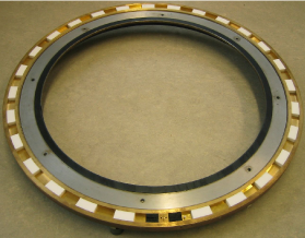
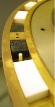
The experimental set-up is shown in figure 1. It consists of a brass ring where a microwave guide is cut out, in which several Teflon pieces, two carbon absorbers, and an antenna are inserted. Another antenna is fixed on the top plate (not shown in the figure) covering the waveguide. The antennas are connected to a network analyzer that allows the measurement of all matrix elements of the scattering matrix. The absorbers are used to eliminate reflection at the ends of the array and hence mimic a 1D scattering system with open ends. This circular wave guide has been used, with metallic screws instead of Teflon pieces, to study the microwave realization of the Hofstadter butterfly [22] and transport properties of 1D on-site correlated disorder potentials [23].
In our experiment, the cut-off frequency for the lowest mode is GHz and the second mode opens at GHz. All results presented in this paper are restricted to the regime of the first propagating mode. Thus the system is effectively one-dimensional. Since the perimeter of the ring ( cm) is much larger than the maximum wavelength used in our experiments ( cm), our theoretical model assumes, as an approximation, a linear set-up (see figure 2).
For the lowest TE mode () at GHz the component of the electric field is also zero and the component is
The wave function obeys the Helmholtz equation
| (1) |
where
| (2) |
and is the position-dependent index of refraction. In the case the Teflon pieces are periodically spaced our system is the electromagnetic counterpart of the quantum 1D Kronig-Penney model.
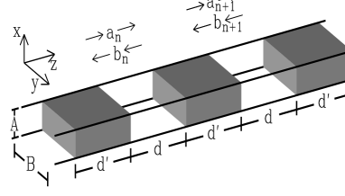
We use the transfer matrix approach to calculate the transmission. Since both antennas are placed in the air, our transfer matrix should connect the wave functions amplitudes from air to air. Referring to figure 2, the transfer matrix for a single cell connects the amplitudes and :
| (3) |
and () denotes the wave vector in air (Teflon pieces) (c. f. equation (2)). The transfer matrix for a single cell are
| (4) | |||||
| (5) |
where
| (6) |
Due to preservation of flow and time reversibility it yields , and . The elements are the same as in the quantum 1D model of a square potential well, but with , and . From (2) ; thus, the Teflon piece acts as a well () in quantum mechanics, except that in the photonic array the “depth” increases with frequency.
The microwave vector network analyzers measure the full scattering matrix defined by
| (7) |
In terms of the matrix elements, the matrix reads
| (8) |
The transmission through a single cell is given by
| (9) |
with and given by Eqs. (4) and (5) for a single cell.
Expression (9) together with equation (5) shows immediately that a single Teflon piece becomes completely transparent at frequencies obeying the relation
| (10) |
We shall refer to these frequencies as 1-Teflon resonances.
For an array of N equally spaced cells without any impurities or defects, we need to evaluate to the power; a numerical process that can be easily performed. However, it is more illustrative to use the Cayley-Hamilton theorem of linear algebra to get [24, 25, 26]
| (11) |
where is the Bloch phase corresponding to the infinitely periodic array:
| (12) |
Note that not only when (i. e., at the 1-Teflon resonances) but also whenever . The latter one gives rise to peaks with in each transmission band since shifts through [24, 25, 26, 27]. According to the above condition, the system of Teflon pieces separated by air becomes transparent when , which in turn implies . We call these the 2-cells resonances emphasizing that it is not just two Teflon pieces next to each other but separated by an air spacing. A little thought reveals that the oscillations are centered around the 2-cells resonance frequency (see also [26]).
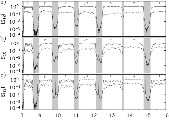
Luna-Acosta et al[25] treat the case of the regular Kronig-Penney model (i. e., periodic and no defects) where it is shown that equation (11) reproduces most details of the experimental transmission data as a function of frequency for all kinds of periodic arrays considered. Since we are concerned here with the effects of the impurities, we show for comparison the theoretical and experimental results for the transmission amplitude for an array 16 equally spaced cells, with Teflon pieces of width =4.0 cm and air spacing of width = 4.0 cm, see figure 3(a).
For the experimental and theoretical curves to agree as well, it was necessary to define some effective length for the length of the Teflon pieces and the air spacings. That is, since the actual waveguide is circular, the Teflon pieces and air spacings are not rectangular pieces but slightly curved with the larger side being exactly 5 percent larger than the shorter side. (The 4 cm Teflon pieces and the air spacings referred to above actually mean that the shorter side is 4 cm whereas the larger one is 4.2 cm.) It turned out that the best fit could be obtained with an effective length of 4.08 cm, i.e, a 2 percent larger than its shorter side. We emphasize that this is the only fitting parameter in our calculations and moreover it is the same for all calculations presented here. Throughout the paper, whenever we quote the width of a Teflon piece or an air spacing we mean the shorter side of it and in the numerical calculations we use their corresponding effective length.
We remark that our model does not consider the absorption of the signal. However, comparison of the experimental and theoretical data shows that the band structure (gaps and band profiles) is not affected by the absorption except for the attenuation of the transmission, which is about constant throughout the frequency range (the experimental transmission is about five times weaker). Thus, absorption in our experiment, does not destroy coherent phenomena like the band structure (see also [23]).
In figure 3 and all subsequent transmission plots the frequency values of the 1-Teflon and 2-cells resonances are marked by crosses and circles, respectively. Different types of bands are formed depending on the position of the Teflon resonances relative to the 2-cells resonances [25]. In these and all forthcoming transmission plots we mark with shaded strips the gap regions, defined by the condition that the eigenvalues of the transfer matrix are real. Since , where , forbidden gaps occur whenever .
Given the good agreement between experimental transmission data and the photonic Kronig-Penney model, implied by equation (11), we proceed to discuss the effects of impurities in the photonic Kronig-Penney model.
3 Impurity effects in the transmission
Different types of defects or impurities can be realized in our experimental set-up with just air and Teflon segments and can be represented by one of the two general sketches shown in figure 4. The upper sketch illustrates a general interstitial impurity: an extra piece of Teflon of width placed somewhere in the air spacing between two pieces of Teflon. The rest of the arrangement remains unaltered; the perpendicular dotted lines mark the boundaries of the unit cell along the pure crystal. By definition of point defect, the interstitial impurity breaks the periodicity only locally. Hence, the length of the extra piece of Teflon should be less than or equal to the air spacing. If the width is larger than this, then the boundaries of the regular cells would be displaced from their original position and consequently periodicity would be globally broken (it becomes an extended defect, e. g., a topological defect [28, 29]). In this paper we do not consider topological defects.


As shown in the upper sketch there are unit cells periodically arranged to the left of point , each described by the matrix , then periodicity is interrupted by the impurity at point and again recovered at point . To the right of point there are cells periodically arranged. The total transfer matrix going from left end of the array to right end of the arrays can be written as
| (13) |
where is the transfer matrix connecting the amplitudes of the wave function at with those at point . Specifically,
| (14) |
where (, and ), is the transfer matrix corresponding to an air spacing, of length . is the transfer matrix for the regular size Teflon piece and that of the Teflon piece of length .Note that , where is the total number of unit cells (and Teflon pieces) of the perfect crystal.
The general case of a single substitutional impurity is shown in the lower sketch of figure 4. The substitutional impurity has a length , shown here longer than the regular size Teflon piece, but it could be of any length and/or of a different dielectric material. Quick inspection shows that the form of the impurity matrix is the same, but the values of the lengths , , and are different and now .
Thus, we have a straight-forward numerical scheme to calculate the transmission amplitude in the presence of an impurity: for a given impurity arrangement we compute equation (13).
In figure 3(b) we show the case when an extra Teflon piece of smaller length (than the length of the default Teflon piece) is inserted in the center of the air spacing between the 3rd and 4th regular Teflon pieces, thus . Figure 3(c) shows the case of the same type of impurity but located in the air spacing between the 8th and 9th regular Teflon pieces, thus . Notice that the good agreement between the transfer matrix calculations and main features of the experimental data.
Inspection of the plots of figure 3 reveals that the impurity affects the transmission in two ways: i) The bands develop different profiles (compared to the pure array, figure 3(a)). ii) Peaks appear in most of the gaps in figure 3(b) coinciding in frequency with those of figure 3(c). Such a coincidence is expected since the impurity in both arrays occupies the same relative position within the cell (in the center of the air spacing) but in a different cell.
In figure 3(b) the band profiles look like a superposition of slow and fast oscillations. In figure 3(c) the oscillations are larger and only of one type. In both, figure 3(b) and (c), bands containing 1-Teflon resonances (see the 2nd, 4th, and 6th bands) are less affected by the impurity. Note also that the intensity of the peaks is greater when the impurity is placed near the center of the array, figure 3(c), than when it is placed near the end of the array, figure 3(b). This feature was invariably found in all our experiments.
Figure 5 shows the experimental and theoretical curves for three types of substitutional impurities. Figure 5(a) pertains to the case when a Teflon is removed from the array, i. e., a vacancy. Specifically, the 8th Teflon is removed. In figure 5(b) the 8th regular size Teflon piece is substituted by a smaller, whereas in (c) it is substituted by a larger one. Note that while the defect is in the same number of cell within the array, the band profiles, the frequencies and intensities of the peaks are different for each case since the defects are different.
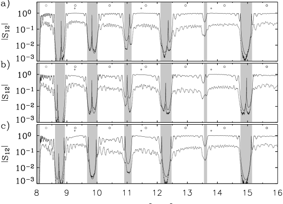
A single point defect can produce multiple impurity levels within a band, as has been observed, e. g. by Yablonovitch et al. [30] in an three dimensional photonic array with a donor-like impurity. Note that the figure 5(c) shows also two spikes in most of the gaps.
Shallow impurities in semiconductors, associated with long-range binding, typically show up as spikes near the band edges, whereas deep impurities typically lie near the center of the gap [18]. However, figure 5 shows that a single impurity may produce spikes near the center of the gap or near the band edges. Thus we see that the above characterization of the impurity as either deep or shallow is not always applicable.
Although our numerical procedure is seen to reproduce quite well the main features of the experimental data, it does not serve to explain their origin. For this purpose we develop a scheme in the next section which provides us with a general understanding of the direct relation between the number of slow and large or fast and small oscillations and the position of the impurities in the array. We will also show how to determine the frequency position of the impurities.
4 Analysis of the effects of the impurities.
We express the transfer matrix in terms of its diagonal representation . Inserting into equation (14) to get
| (15) |
where
| (16) |
with , , and
Note that is the impurity matrix in the representation of the diagonal basis of . This “rotated impurity matrix” contains information about the coupling of the impurity to the host material through the elements of the transformation matrix .
From the definition of and using the representation of given above we get after some algebra useful expressions for the matrix elements of :
| (17) |
where ,
| (18) |
and
| (19) |
The terms and are obtained from and , respectively, by exchanging with everywhere. As in the case of a single scatterer, it is also true that the complex conjugate of () is (). This property is not obeyed by the elements of the rotated impurity matrix. On the other hand, because equation (16) is a unitary transformation, and .
Setting , and in equation (16) and using we recover equation (11) that is valid only for the pure array.
4.0.1 Band oscillations
To analyze the effects of the impurity on the band profiles it is convenient, since , to study in detail the element given by equation (17). In the bands the eigenvalues are complex, and of modulus one, so we can (when considering the absolute value of ) ignore from our analysis the factor in front of expression (17). We now discuss the quantities and . The functions do not contain any information on the impurity: they depend only on and , characterizing the periodic array. are real and smooth ( almost flat) functions within the bands, diverging as at the band edges 111In the bands: with real, and can be written as . It follows from the definition of that and . Given that and are smooth functions everywhere and goes to zero at the band edges (where ) then are very smooth functions within the bands, diverging as at the band edges.. More important for our analysis is to note that and take alternate roles in consecutive bands. Namely, is larger than in the first and all odd-numbered bands, while the opposite is true in the second and all even-numbered bands.
The quantities are also typically very smooth functions within the bands, diverging like at the band edges, and are all roughly of the same magnitude, except for which diverges at the Teflon resonance (but note that at Teflon resonances).
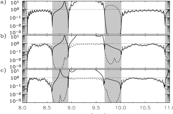
With this information about the and it is expected that in the odd-numbered bands, where terms containing can be ignored to first order, the first two terms in equation (17) give the main contribution to . Specifically, should yield oscillations (recall that shifts through in each band). Figure 6(a) shows this term and also as a function of frequency for the case of an interstitial impurity centered between the third and fourth Teflon piece (the case corresponding to figure 3(b)). For the moment let us concentrate on the first and third transmission band. The term (dashed curve in (a)) gives the zero order approximation to the transmission band. According to the notation of figure 4 it follows that and . The 12 oscillations can be counted in figure 4(a) in the plot of . Moreover, since gives the dominant contribution in the odd-numbered bands, the oscillations should also be observed in the total transmission. Indeed this is the case, as it is shown by the dashed curve in figure 6(b). This plot also shows that the total transmission curve oscillates about a slowly oscillating curve (thick solid line) with two maxima. This slowly oscillating curve is in fact given by with as pointed out above. Finally the last term in equation (17) gives additional oscillations of smaller amplitude, which provide small corrections (not readily visible in the plot).
As figure 6(b) shows, the term does not agree at all with the average curve of the transmission in the gaps nor in the even numbered bands. This is because our discussion has been limited to the bands, where the eigenvalues are complex, and of modulus one, whereas in the gaps the eigenvalues are real, and hence the factor in (17) cannot be ignored (in the next section we shall consider in detail the gap regions). There is no agreement in the even-numbered bands either because there the dominant terms are those containing the form factor , namely, the sum . This can be readily seen by factoring in equation (17) the term to get . Written in this form, it is clear that the same arguments used for the odd-numbered bands work for the even numbered bands but with and interchanged. Explicitly, the dominant term in the even-numbered bands is , giving rise again to oscillations. The second order term, producing the oscillations, is .
Thus, the number of slow and fast oscillations appearing in the profiles of the transmission bands can be read off directly from equation (17). Assuming for the moment that , the band profiles should show fast oscillations about a curve with slow oscillations. This is exactly what we have noticed in our experimental and numerical transmission curves, see, e. g., figure 3(b), corresponding to an interstitial impurity with , respectively.
On the other hand, if , then the profile should show only oscillations of larger amplitude than in the case above (). The experiments confirm this, as it is illustrated in figure 3(c), where . Finally, if is close but not exactly equal to then the oscillation pattern becomes more complicated, with irregular (incomplete) oscillations and with no distinctive modulation pattern, as exemplified by the plots of figure 5, where =6 and =8.
Thus, given some experimental curves for the transmission, one can determine where along the array there is a single impurity by simply observing the pattern and number of oscillations. Note, however, that due to time reversal symmetry it is not possible to deduce on which side of the array to count the cells. At the very least, the form of the profile indicates the presence of impurity or defect, and whether it is located near the ends or near the center of the array.
It is important to remark that the above conclusions hold as long as the elements do not have oscillations of their own as it is the case of the interstitial impurities discussed above. For certain other types of defects the elements do have some structure and consequently the type of profiles discussed above become somewhat distorted. An extreme example occurs when a smaller Teflon piece is placed off-center between two regular size Teflon pieces, that is, a displaced interstitial impurity. Specifically, show a strong frequency dependence (e. g., and have each three extrema in their real and imaginary parts in each band). For example, figure 6(c) shows the total transmission and for an interstitial impurity placed off-center between the 3rd and 4th regular size Teflon. This defect is described by the upper sketch of figure 4 with and with . Note that the term correctly gives the average curve of the band profile but now there are three slow oscillations and 14 fast oscillations, instead of 2 and 12 oscillations, respectively.
4.0.2 Impurity states
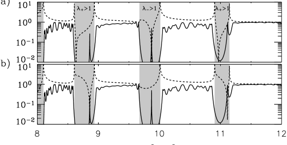
We now analyze the appearance of the peaks in the gaps, the well known signal for the presence of an impurity. Without limiting in any way the conclusions to be drawn here, let us consider the 4 cm array, the example we have been using, and let us label the gaps. Gap one is in the frequency range [7.7, 8.1] GHz, see, e. g., figure 7; gap two in the range GHz, and so on.
Recall that in the gaps the eigenvalues are real, therefore, we rewrite equation (17) as
| (20) |
where . Now, for the transmission to produce a sharp peak in the gaps, must be small in a very narrow range of frequencies. Note that , with and alternatingly being the larger one in each gap. In the even-numbered gaps (where ) the dominant term in is the first term in equation (20), and it will be large (corresponding to a negligible transmission) unless it happens that is very small or zero. Similarly, in the odd-numbered gaps (where ), the dominant term is the last one and it will also be a large number unless happens to be very small. To illustrate this general observation, in figure 7 we consider the case of an interstitial impurity placed in the air spacing of the 8th cell in a 16-cell array (thus, ). In figure 7(a) we show the transmission amplitude and also the term . In contrast, in (b) the term is shown, together with . Observe in figure 7(a) that whenever goes sharply to zero in the odd-numbered gaps (), there is an impurity state at the same frequency. also goes to zero sharply in the even-numbered gaps() but here there is no coincidence with the impurity states, in agreement with our argument of the previous paragraph. Similarly, figure 7(b) shows that there is an impurity state in the even-numbered gaps at the frequency values where goes to zero. Thus, our simple argument above really works in determining the position of the impurity states: an impurity state occurs in odd-numbered gaps at the frequencies where is zero and in the even-numbered gaps where is zero. A similar case was already shown in figure 3(c) except there ( and thus band profiles are different but peak positions are the same), where we see an excellent agreement with experiment concerning the location of the peaks.
Single impurity states are known to decay exponentially away from the site of the impurity. One then may expect that the intensity of the peak should be stronger the closer the impurity is from any of the ends of the array. However close inspection of formula indicates that this is not the case. That is, exactly at the impurity state frequency, say when is zero in an even-numbered band, the first term in (20) is zero and the leading terms are . The inverse of its absolute value gives to a good approximation the intensity of the peak. For simplicity, let us consider first the case which is valid only for “symmetric impurities”, i. e., when the distance equals the distance (see figure 4). Note that as a function of is symmetric about its minimum . Thus, recalling that the transmission is the reciprocal of , we conclude that the intensity of the impurity state should be stronger the closer the impurity is to the center of the array. It is strongest when , i. e., when the impurity or defect is at the center of the array.
The above argument assumed that the impurity is symmetric. If it is not the case, then it can be shown that the minimum of does not occur when the impurity is at the center () but at a distance that is proportional to the logarithm of . Since this ratio is not large, the highest intensity peak occurs still when the impurity is close to the center of the array. This was verified in all our experiments and can be seen clearly by comparing figure 3(b) and figure 3(c). We emphasize that this effect is independent of the type of the periodic potential and type of impurity in a 1D periodic array. In fact, the same behavior was noted in an experiment with a coaxial connector photonic crystal [19] where, however, no explanation was given.
As we have seen, the intensity of the peaks always decreases as the number of cells increases. However, an important conclusion, drawn from a detailed examination of equation (20) as a function of , for fixed , is the following: the decrement in the peak intensity as increases is weaker the farther the impurity state is from the center of the transmission band. This was confirmed by our experimental and theoretical results and it is in agreement with the generally accepted idea that shallow states near the band edges are the shallow levels, associated with long range potentials, in contrast with the deep levels lying near the center of the band (see, e.g.,[18]).
5 Conclusions
We analyzed the effects on the transmission of single impurities in an array of regularly spaced pieces of Teflon in a microwave guide, described by a 1D photonic Kronig-Penney Model. We performed a series of experiments with point defects of various types; namely, interstitial, substitutional, and vacancies and showed that single impurity affects the transmission in two ways. One is the well known appearance of localized states in the gaps; the second, to our knowledge not discussed so far in the literature, is the appearance of fast and slow oscillations in the band profiles. Our transfer matrix calculations correctly predicted these features. Experiments with other types of single impurities, e. g., displaced interstitial and displaced substitutional impurities, not reported here, were also found to be equally well described by our model. The transfer matrix calculations (being purely numerical) agree very well with the experimental data, but they provide no insight for the understanding of the various features observed. Thus, as an important contribution, we derived an exact closed form expression for the transmission amplitude that is useful in elucidating the effects of a single impurity on the band profiles, the impurity levels, and their intensity. This expression involves elements of the transfer matrix of the regular cells in the array and of the transfer matrix of the impurity. Since this matrix is written in the representation that diagonalize the transfer matrix of the regular cells, contains information about the impurity and its coupling with the host environment. We found that the set of impurity levels is given by the zeroes of the diagonal elements of . Further it was shown that the intensity of the impurity states in the gaps depends on two factors, namely, the off-diagonal elements of and the distance of the impurity from the center of the array. The closer the impurity is to any of the ends of the array, the lower the intensity of its level, and vice versa. It was also shown that the number of fast and slow oscillations in the bands give direct information about the position of the impurity, relative to the center of the array.
We note that the agreement between the experimental results and analytical calculations gives us confidence to treat the inverse problem. That is, we can extract information about the unknown defect from the inspection of the band profiles and the localized defect modes. Our method is an alternative approach to the tight-binding and Green’s functions methods, for 1D systems, with the advantage that it is simpler and elucidating. Although the experimental realization here is in the microwave regime, the model and the results are equally valid for higher scales of frequency corresponding to light experiments. We remark that we can apply our formalism in a straight-forward manner to any kind of regular array with single defects once we have determined the particular transfer matrices for the regular cell and for the impurity.
We emphasize that the formulas (17-20) and the procedure for determining the position and intensity of impurity states and features of the band profiles for the photonic Kronig-Penney model are exactly the same as for the electronic Kronig-Penney model (with square barriers) for energies above the barrier. This is so since their transfer matrix elements are identical and the difference is only in the definition of the longitudinal wave vector. Hence our procedure is useful for analyzing the effects of impurities either, in the transport of charged particles in 1D periodic arrays of electronic potentials (e. g., heterostructures) or the transmission of electromagnetic waves in 1D photonic arrays.
Finally, the fact that our experimental and theoretical results agree very well give us confidence to treat various other types of specific arrangements with the goal of realizing them in other experimental set-ups as photonic devices. We would like to stress that this is by no means self evident. The observed transmission patterns are the result of a complicated interplay of interferences from all structures within the waveguide, and it is well known that interferences are extremely sensitive to perturbations, in particular in the presence of absorption. The present work has shown that we can rely on the experiment in this respect. Thus our experimental set-up can be used as a preliminary — and low cost — study of a particular Kronig-Penney model to be implemented later in more sophisticated and expensive microscopic photonic realizations, which might have real applications.
Acknowledgments
One of the authors (G.A.L-A) is grateful to the DFG, Germany, for the economic support via the Mercator Professorship and to Prof. Stöckmann and his group for their hospitality. The experiments were supported by the DFG. G. A. L-A also acknowledges partial support from SEP-CONACYT Convenio P51458.
References
- [1] E. Yablonovitch. Inhibited spontaneous emission in solid-state physics and electronics. Phys. Rev. Lett., 58:2059, 1987.
- [2] S. John. Strong localization of photons in certain disordered dielectric superlattices. Phys. Rev. Lett., 58:2486, 1987.
- [3] J. D. Joannopoulos, R. D. Meade, and J. N. Winn. Photonic Crystals: Molding the flow of light. Princeton Univ. Press, Princeton, New Jersey, 1995.
- [4] S. G. Johnson and J. D. Joannopoulos. Photonic Crystals: The Road from Theory to Practice. Kluwer, Dordrech, 2002.
- [5] M. Bayindir, B. Temelkuran, and E. Ozbay. Propagation of photons by hopping: A waveguiding mechanism through localized coupled cavities in three-dimensional photonic crystals. Phys. Rev. B, 61:R11855, 2000.
- [6] L. Xu-Sheng, H. Chong, O. Yan-Dong, and L. Sheng. Tolerance of photonic crystal impurity bands to disorder of defects in coupled cavity waveguides. Chin. Phys. Lett, 21:863, 2004.
- [7] M. Qi, E. Lidorikis, P. T. Rakich, S. G. Johnson, J. D. Joannopoulos, E. P. Ippen, and H. I. Smith. A three-dimensional optical photonic crystal with designed point defects. Nature, 429:538, 2004.
- [8] D. L. C. Chan, E. Lidorikis, and J. D. Joannopolous. Point defect geometries in inverted opal photonic crystals. Phys. Rev. E, 71:056602, 2005.
- [9] S. G. Johnson and J. D. Joannopoulos. Block-iterative frequency-domain methods for Maxwell’s equations in a planewave basis. Optics Express, 8:173, 2001.
- [10] K. S. Kunz and R. J. Luebbers. The Finite Difference Time Domain Method for Electromagnetics. CRC Press, Boca Raton, Florida, 1993.
- [11] J. M. Elson and P. Tran. Coupled-mode calculation with the -matrix propagator for the dispersion of surface waves on a truncated photonic crystal. Phys. Rev. B, 54:1711, 1996.
- [12] J. B. Pendry and A. MacKinnon. Calculation of photon dispersion relations. Phys. Rev. Lett., 69:2772, 1992.
- [13] M. G. Khazhinsky and A. R. McGurn. Green’s function method for waveguide and single impurity modes in 2d photonic crystals: H-polarization. Phys. Lett. A, 237:175, 1998.
- [14] K. Sakoda. Optical Properties of Photonic Crystals. Springer-Verlag, New York, 2001.
- [15] C. Kittel and A. H. Mitchell. Theory of donor and acceptor states in silicon and germanium. Phys. Rev., 96:1488, 1954.
- [16] J. M. Luttinger and W. Kohn. Motions of electrons and holes in perturbed periodic fields. Phys. Rev., 97:869, 1955.
- [17] H. Nozaki and S. Itoh. Energy correction for isolated impurities under periodic boundary conditions. Phys. Rev. E, 62:1390, 2000.
- [18] J. G. Menchero, R. B. Capaz, B. Koiler, and H. Chacham. Tight-binding scheme for impurity states in semiconductors. Phys. Rev. B, 59:2722, 1999.
- [19] R. D. Pradhan and G. H. Watson. Impurity effects in coaxial-connector photonic crystals: A quasi-one-dimensional periodic system. Phys. Rev. B, 60:2410, 1999.
- [20] S. L. McCall, P. M. Platzman, R. Dalichaouch, D. R. Smith, and S. Schultz. Microwave propagation in two-dimensional dielectric lattices. Phys. Rev. Lett., 67:2017, 1991.
- [21] L. P. Kouwenhoven, F. W. J. Hekking, B. J. van Wees, C. J. P. M. Harmans, C. E. Timmering, and C. T. Foxon. Transport through a finite one-dimensional crystal. Phys. Rev. Lett., 65:361, 1990.
- [22] U. Kuhl and H.-J. Stöckmann. Microwave realization of the Hofstadter butterfly. Phys. Rev. Lett., 80:3232, 1998.
- [23] U. Kuhl, F. M. Izrailev, A. A. Krokhin, and H.-J. Stöckmann. Experimental observation of the mobility edge in a waveguide with correlated disorder. Appl. Phys. Lett., 77:633, 2000.
- [24] D. J. Griffiths and C. A. Steinke. Waves in locally periodic media. Am. J. Phys., 69:137, 2001.
- [25] G. A. Luna-Acosta, H. Schanze, U. Kuhl, and H.-J. Stöckmann. Preprint. to be published.
- [26] D. W. L. Sprung, H. Wu, and J. Martorell. Scattering by a finite periodic potential. Am. J. Phys., 61:1118, 1993.
- [27] F. Barra and P. Gaspard. Scattering in periodic systems: from resonances to band structure. J. Phys. A, 32:3357, 1999.
- [28] L. Gumen, E. Feldman, V. Yurchenko, A. Krokhin, and P. Pereyra. Topological defects in 1D potential and superlattices. Physica E, 17:264, 2003.
- [29] A. Morales, R. A. Méndez-Sánchez, and J. Flores. Topological defects in 1D elastic waves. Physica E, 19:289, 2003.
- [30] E. Yablonovitch, T. J. Gmitter, R. D. Meade, A. M. Rappe, K. D. Brommer, and J. D. Joannopoulos. Donor and acceptor modes in photonic band structure. Phys. Rev. Lett., 67:3380, 1991.