Geometry dependence of the charge transfer at YBa2Cu3O7-metal interfaces
Abstract
Transport in electronic devices based on high-Tc superconductors depends critically on the charge redistribution at interfaces, since the band structure is modified on a local scale. Using the density functional theory approach for relaxed YBa2Cu3O7-metal contacts, the charge transfer into the superconductor has been studied in Appl. Phys. Lett. 90, 192502 (2007). In the present paper we discuss the systematics inherent in the local electronic structure of the near-contact YBa2Cu3O7 sites, in particular the dependence on the contact geometry.
pacs:
73.40.Jn, 74.25.Jb, 74.72.BkI Introduction
Due to large dielectric constants and small carrier samara90 densities, electronic transport in wires and tapes from high-Tc materials is seriously affected by structural defects and interfaces mannhart98 ; hilgenkamp02 . Moreover, the specific contact resistivity of YBa2Cu3O7(YBCO)-metal thin films is determined by details of the contact geometry hahn94 and the transport in micron-sized YBCO-metal heterojunctions depends on the orientation of the YBCO crystallographic axes with respect to the direction of the current flow komissinskii01 . Unexpected high specific resistivities of YBCO-Au interfaces, to at low temperatures xu04 , presumably result from local distortions at the interface. While theoretical attempts to describe the charge distribution at such interfaces are rare, the linear background and asymmetry in the differential conductance of a tunnel junction between a high-Tc superconductor and a metal can be explained by inelastic scattering grajar97 . In addition, the charge imbalance at the boundary of a short coherence length superconductor and a normal metal is accessible to a self-consistent microscopic approach nikolic02 .
II Technical details
Taking into account the details of the crystal structure, the electronic properties of YBCO-metal interfaces can be addressed by means of first principles band structure calculations us07c . In this paper we investigate the dependence of the local electronic structure in the YBCO domain on the contact geometry. As YBa2Cu3O7 belongs to the overdoped regime, our interfaces are metallic. The calculations are based on density functional theory and the generalized gradient approximation, as implemented in the WIEN program package wien2k , which is suitable for dealing with structural relaxation and charge redistribution at surfaces and interfaces us07a ; us07b . Because band-bending is proposed to take place on the length scale of the YBCO lattice constant, the electronic structure of YBCO-metal interfaces becomes accessible to a supercell approach with periodic boundary conditions. Due to a minimal lattice mismatch of %, it is convenient to choose fcc Pd as metallic substituent.


We study interfaces oriented parallel and perpendicular to the CuO2 planes. The parallel interface is modelled by means of a supercell consisting of two YBCO unit cells along the crystallographical -axis, terminated by the CuO-chain layer xin89 ; derro02 , and four metallic unit cells stacked in [001] direction. However, the results are closely related to those for BaO terminated YBCO. The perpendicular interface consists of three YBCO unit cells and a metallic supercell stacked in [010] direction. In total, the supercell therefore contains 9 metallic unit cells. We again choose a CuO/Pd interface to prepare for comparison with the parallel configuration. In contrast to the latter, oxygen atoms from the BaO planes and copper atoms from the CuO2 planes here likewise touch the metal layer. Giving rise to the main difference between the two configurations, in the parallel configuration the CuO2 planes are well separated from the metal by an almost insulating BaO layer, whereas they are in contact in the perpendicular configuration. The Y atoms are in touch with the metal layer only in the latter case. Relative shifts between the YBCO and metal domain parallel to the interface have minor effects. We start from the experimental bulk YBCO lattice constants Å and Å siegrist87 , and optimize the atomic coordinates in a first step kouba99 . Parallel to the interface, the YBCO lattice constants are used for the palladium domain, too. In the perpendicular direction, we apply the fcc Pd lattice constant Å. In a second step, the structural relaxation of the supercells is carried out, see us07d for details of the structure optimization.
III Results
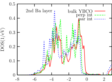
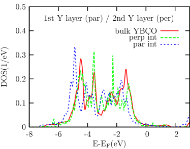
In the following discussion, we compare the electronic structures of our YBCO-metal interfaces with results of a bulk YBCO calculation (which agree perfectly with previous findings pickett89 ). In addition, we will concentrate on atomic sites slightly off the YBCO-metal contact, in order to determine a common behaviour. These sites are less affected by the structural optimization, whereas the electronic properties of atoms right at the interface depend strongly on structural subtleties and therefore are not of interest here. We first study the partial density of states (DOS) associated with the Ba and Y electron donor sites, see the DOS curves in fig. 1. For both geometries, the 2nd Ba layer off the interface is well separated from the metal domain. As a consequence, the gross features of the DOS curves agree well with each other as well as with the bulk YBCO DOS, when an adequate energetical shift of about eV is applied. In contrast, the Y DOS curves hardly coincide, which traces back to large differences in the local atomic environments of the Y sites in the parallel and perpendicular interface configuration. The 1st Y layer off the parallel interface is well separated from the metal by four atomic layers. The energetical shift of the Y states therefore can be attributed to strong down-bending of the electronic bands due to a modified Fermi level. At the perpendicular interface, Y-Pd orbital overlap suppresses band-bending effects. While the Y DOS reveals a finite number of states at the Fermi level, the Ba DOS almost vanishes. Electronic screening thus is less efficient at the Ba sites and the band-bending amplitude increases.


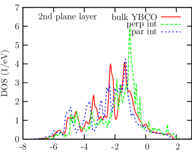
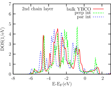
Turning to the copper sites, the gross structure of the Cu DOS is hardly affected by the interface, see fig. 2. The second layer Cu atoms largely resemble the bulk DOS and therefore allow us to study the band-bending. Concerning the CuO-chain sites, results for the parallel and perpendicular interface configuration agree quite well. Similar to the discussion of the Y DOS, the smaller energy shift in the perpendicular case can be explained by direct Cu-Pd orbital overlap. Understanding the DOS shape of the CuO2-plane sites is less intuitive. For the parallel interface, we observe almost perfect agreement of the DOS curves, whereas some effects of the structural relaxation are left for the perpendicular interface. However, in both cases the bulk DOS has to be shifted to lower energies in order to reconcile the curves, which we again interpret in terms of down-bending of the electronic bands. The necessary shifts amount to 0.20 eV and 0.15 eV in the parallel and perpendicular case, respectively. As a consequence, the hole count at the Cu sites in the CuO2-planes is altered, where the 0.20 eV shift corresponds to a reduction of 0.13 holes and the 0.15 eV shift comes along with a reduction of 0.09 holes. Since the charge transfer depends only little on the orientation of the YBCO-metal interface with respect to the high-Tc unit cell, an intrinsic doping close to 0.1 eV seems to be characteristical for YBCO-metal contacts. As a consequence, the system is shifted into the underdoped regime of the YBCO phase diagram, which is expected to be reflected by transport properties, like the current in tunneling experiments.
IV Conclusion
In conclusion, we have discussed electronic structure calculations for prototypical interfaces between the short coherence length superconductor YBa2Cu3O7 and a normal metal. We find that the charge redistribution induced by the metal contact can be interpreted in terms of an intrinsic doping of the superconductor on a nanometer length scale. This fact corresponds well with the experimental observation of charge carrier depletion. The net charge transfer in favour of the copper sites in the CuO2-planes amounts to some 0.1 electrons, with only a weak dependence on the orientation of the interface. We expect that the reported charge transfer amplitude applies to any contact geometry as long as the YBCO domain terminates with a copper/oxygen layer.
Acknowledgements.
We acknowledge valuable discussions with U. Eckern, V. Eyert, J. Mannhart, and T. Kopp, and financial support by the Deutsche Forschungsgemeinschaft (SFB 484).References
- (1) G.A. Samara, W.F. Hammetter, and E.L. Venturini, Phys. Rev. B 41, 8974 (1990).
- (2) J. Mannhart and H. Hilgenkamp, Mater. Sci. Eng. B 56, 77 (1998).
- (3) H. Hilgenkamp and J. Mannhart, Rev. Mod. Phys. 74, 485 (2003).
- (4) R. Hahn, J. Klockau, and G. Fotheringham, Supercond. Sci. Technol. 7, 290 (1994).
- (5) F.V. Komissinskii, G.A. Ovsyannikov, and Z.G. Ivanov, Phys. Solid State 43, 801 (2001)
- (6) Y. Xu and J.W. Ekin, Phys. Rev. B 69, 104515 (2004).
- (7) M. Grajcar, A. Plecenik, P. Seidel, V. Vojtanik, and K.U. Barholz, Phys. Rev. B 55, 11738 (1997).
- (8) B.K. Nikolić, J.K. Freericks, and P. Miller, Phys. Rev. B 65, 064529 (2002).
- (9) U. Schwingenschlögl and C. Schuster, Appl. Phys. Lett. 90, 192502 (2007).
- (10) P. Blaha, K. Schwarz, G. Madsen, D. Kvasicka, and J. Luitz, WIEN2k, An augmented plane wave + local orbitals program for calculating crystal properties (TU Wien, 2001).
- (11) U. Schwingenschlögl and C. Schuster, Chem. Phys. Lett. 435, 100 (2007); ibid. 439, 143 (2007).
- (12) U. Schwingenschlögl and C. Schuster, submitted for publication.
- (13) G. Xin-Gao and Z. Qing-Qi, J. Phys.: Condens. Matter 1, 593 (1989).
- (14) D.J. Derro, E.W. Hudson, K.M. Lang, S.H. Pan, J.C. Davis, J.T. Markert, and A.L. de Lozanne, Phys. Rev. Lett. 88, 097002 (2002).
- (15) T. Siegrist, S. Sunshine, D.W. Murphy, R.J. Cava, and S.M. Zahurak, Phys. Rev. B 35, 7137 (1987).
- (16) R. Kouba, C. Ambrosch-Draxl, and B. Zangger, Phys. Rev. B 60, 9321 (1999).
- (17) U. Schwingenschlögl and C. Schuster, Europhys. Lett. 77, 37007 (2007).
- (18) W.E. Pickett, Rev. Mod. Phys. 61, 433 (1989).