Theory of shot noise in single-walled metallic carbon nanotubes weakly coupled to nonmagnetic and ferromagnetic leads
Abstract
We present theoretical study of shot noise in single wall metallic carbon nanotubes weakly coupled to either nonmagnetic or ferromagnetic leads. Using the real-time diagrammatic technique, we calculate the current, Fano factor and tunnel magnetoresistance in the sequential tunneling regime. It is shown that the differential conductance displays characteristic four-fold periodicity, indicating single-electron charging. Such a periodicity is also visible in tunnel magnetoresistance of the system as well as in the Fano factor. The present studies elucidate the impact of ferromagnetic (vs. nonmagnetic) contacts on the transport characteristics under consideration.
pacs:
72.25.Mk, 73.63.Kv, 85.75.-d, 73.23.HkI Introduction
In connection with more and more demanding miniaturization requirements of the modern electronics, there has recently been much interest in electric transport in low-dimensional nanostructured materials like quantum dots and quantum wires (both conventional kouwenhoven01 ; harrison99 and magnetic wolf01 ; loss02 ; maekawa02 ; zutic04 ; maekawa06 ; sanvito06 ). Similarly, carbon nanotubes (CNTs) have been attracting wide attention for more than one and a half decade due to their exceptional transport and mechanical properties.saito98 In particular, depending on how a graphite monolayer (graphene) is rolled up into a cylinder, the resulting nanotube may be either metallic or semiconducting. CNTs may be used as interconnects as well as switching and nonvolatile memory devices in nanoelectronics. anantram06 ; hoenlein Furthermore, there is no doubt that CNTs are also quite promising for spintronic applications, because when placed between ferromagnetic electrodes they show a considerable giant (tunnel) magnetoresistance, GMR (TMR), ranging from a few, up to several tens percent. tsukagoshi99 ; zhao02 ; kimPRB02 ; sahoo05 ; jensenPRB05 ; manPRB06 ; liuPRB06 ; nagabhiravaAPL06 ; krompiewski05 ; krompiewski06 ; cottetPRB06 ; cottet06 ; schonenberger06 Moreover, recent experiments on single wall CNTs with moderate coupling to external leads sahoo05 have shown that TMR in nanotubes can become negative. This behavior was accounted for theoretically in terms of spin-dependent phase shifts at interfaces. cottetPRB06 Therefore our theoretical analysis of CNTs is extended so as to include, on the one hand detailed intrinsic energy-level structure of the given CNT (singlet vs. triplet energy level occupancies, etc.), and on the other hand the effect of magnetic electrodes on transport properties. It is now well-known that at low temperature the Coulomb blockade regime may manifest itself even when the so-called addition energy is less than energy-level spacings. As shown in Refs. [liangPRL02, ; sapmazPRB05, ], the conductance spectra of CNTs in that case reveal a characteristic four-fold structure with relatively high peaks (of the order of ).
In this paper we analyze theoretically the charge and spin transport in single wall CNTs weakly coupled to metallic leads – either nonmagnetic or ferromagnetic. We consider Coulomb blockade transport regime, where the mean-field model of Oreg et al. oregPRL00 is applicable. That is the case when the charging energy-to-mean level spacing ratio is small enough (and consequently the Luttinger parameter in not drastically less than 1) - otherwise, the Luttinger-liquid model would be more appropriate. egger ; kane ; bockrath Our considerations are based on the real-time diagrammatic technique. Assuming realistic parameters of the system, liangPRL02 ; sapmazPRB05 we calculate the basic transport characteristics, i.e. the current, conductance, and TMR in the case of ferromagnetic contacts. Apart from this, we also calculate the shot noise (associated with discrete nature of charge) and show that the corresponding Fano factor is suppressed below the Schottky value, , beyond the Coulomb blockade regime. More specifically, in the transport regions where sequential contribution to the current is dominant, the shot noise is sub-Poissonian with slightly above 0.5. Since our considerations are limited to the first-order transport with respect to the coupling parameter, the above conclusion does not apply to regions where sequential tunneling processes are exponentially suppressed. It is noteworthy that the linear and nonlinear transport across carbon nanotubes has been recently addressed by Mayrhofer and Grifoni. mayrhoferPRB06 ; mayrhoferEPJB07 These considerations however deal with the case of (i) nonmagnetic leads, and (ii) basically large diameter nanotubes, for which both the exchange effects and back scattering processes can be neglected. Spin-polarized transport for collinear and noncollinear alignments of the leads’ magnetic moments was discussed in Refs. [cottet06, ; koller07, ]. However, the considerations presented in Ref. [koller07, ] are again subjected to the constraints (ii), whereas Ref. [cottet06, ] concerns only the linear response regime (zero bias limit). In the present paper we focus mainly on the shot noise, using a nonequilibrium approach applicable, in principle, to carbon nanotubes of arbitrary diameter. It seems that, at present, theoretical studies on the shot noise in CNTs lag behind recent experimental ones (e.g. [onac06, ; wu07, ; tsuneta07, ]). On the other hand, we are not aware of any investigations (either theoretical or experimental) on the shot noise in ferromagnetically contacted CNTs. Therefore, the main objective of this study is to fill, at least partially, these gaps. In addition, we also believe that our considerations will stimulate experimental research on CNTs weakly coupled to ferromagnetic leads, and will be helpful in understanding future experiments.
The paper is organized as follows: In Sec. II the model and computational method are shortly described. Sections III and IV present results on electronic transport (including the shot noise) in the sequential tunneling approximation for nonmagnetic and ferromagnetic contacts, respectively. Finally, Sec. V provides a short summary and conclusions.
II Model and method
The system considered in this paper consists of a single wall metallic CNT and two electron reservoirs (electrodes) which are weakly coupled to the CNT. The electrodes can be either nonmagnetic or ferromagnetic. In the latter case, the net spin moments (and magnetizations) of the leads are assumed to be collinear, i.e., they can form either parallel or antiparallel magnetic configuration. The Hamiltonian of the system takes the general form
| (1) |
The first two terms describe noninteracting itinerant electrons in the leads,
| (2) |
for the left () and right () lead, with being the energy of an electron with the wave vector and spin in the lead , and () denoting the respective creation (annihilation) operator.
The third term, , in the Hamiltonian, Eq. (1), describes the CNT and is assumed in the form introduced by Oreg et al. oregPRL00
| (3) | |||||
where , and () is the creation (annihilation) operator of an electron with spin on the th level in the subband (). The discrete structure of the energy levels results from the quantization of electron motion along the CNT, which is an appropriate starting point in the limit of weak coupling between the nanotube and the leads. The corresponding energy of the th discrete level in the subband is given by , where is the mean level spacing and describes the energy mismatch between the discrete levels corresponding to the two subbands. The second term in Eq. (3) stands for the electrostatic energy of a charged CNT, with denoting the charging energy and being the charge on the nanotube induced by gate voltages. The next term corresponds to the on-level Coulomb interaction with being the relevant on-site Coulomb parameter. Finally, the last term in Eq. (3) describes the exchange energy, with being the relevant exchange parameter. Furthermore, the system is symmetrically biased and we assume equal capacitive couplings to the left and right leads, so the dependence of the nanotube energy levels on the bias voltage may be neglected. The exchange effects described by play an important role for small diameter nanotubes (up to 2 nm or so), whereas for nanotubes of larger diameters these effects become negligible. Thus in the latter case transport properties can be qualitatively described without taking into account the exchange interaction. mayrhoferPRB06 ; mayrhoferEPJB07 Incidentally we show in the following that happens to be rather small in the present model, too. We also notice that the mean-field model of Oreg et al. oregPRL00 , Eq. (3), can be used to analyze the ground state properties and particle-hole excitations of single wall carbon nanotubes, however it fails to describe collective excitations such as spin and charge density waves, spin-charge separation, etc. (Luttinger liquid behavior). egger ; kane ; bockrath
The last term of Hamiltonian, , takes into account tunneling processes between the CNT and electrodes, and is assumed in the form,
| (4) |
where denotes the tunnel matrix elements between the lead and the th level (assumed to be spin-independent also for ferromagnetic leads). The th level coupling to external leads can be described by , with being the density of states in the lead for spin . The role of ferromagnetic leads is taken into account just via the spin-dependent density of states . By introducing the spin polarization of the lead , , the coupling parameters can be expressed as , with . Here, and describe the coupling of the th level to the spin-majority and spin-minority electron bands of the th lead, respectively. When the leads are nonmagnetic, then . In the following we assume for all values of the indices and .
We analyze electronic transport through the single wall metallic CNT described by the Hamiltonian (3), and the considerations are limited to the sequential (first order in tunneling processes) tunneling regime. The first-order tunneling gives the dominant contribution to the charge and spin currents for voltages above a certain threshold voltage, and is exponentially suppressed in the Coulomb blockade regime. The effects due to higher-order tunneling processes, e.g. cotunneling, cotunneling ; weymannPRB07 ; weymannPRB05 are not taken into account. When the bias voltage exceeds the threshold voltage, the current flows due to tunneling of electrons one by one through the discrete energy levels of the nanotube. In order to make the analysis most realistic, in numerical calculations we have taken into account up to six different orbital levels, three in each subband, which results in many-body nanotube states .
Transport is calculated with the aid of the real-time diagrammatic technique. diagrams ; thielmann ; weymannPRB05 This technique consists in a systematic perturbation expansion of the reduced density matrix and current operator in the couplings . To determine the stationary occupation probabilities, charge current, and shot noise in the sequential tunneling regime, we employ the matrix approach developed in Ref. [thielmann, ], and introduce the respective self-energy matrices: , , . The matrix contains self-energies with one arbitrary row replaced by , which is due to the normalization of the probabilities, . The elements of the matrix describe the first-order tunneling transitions between the and many-body states. They are given by, thielmann , where
for and , with and being the electrochemical potential of the lead . The second matrix, , denotes the full self-energy matrix with one internal vertex, associated with the expansion of the tunneling Hamiltonian, replaced by the current operator. Finally, the third matrix, , consists of self-energies with two internal vertices replaced by the current operator. The current operator is defined as , with being the current flowing from the nanotube into the lead . The elements of the matrices and can be expressed in terms of as, thielmann and , respectively, where and is the step function.
Having calculated the respective matrices, the stationary probabilities can be determined from the following equation, thielmann
| (5) |
where is the vector containing the occupation probabilities. In turn, the sequential current flowing through the CNT can be calculated from
| (6) |
with denoting the trace of the matrix . On the other hand, the zero-frequency shot noise, , is given by
| (7) |
where is determined from the equation , with . thielmann
Having found the current and the zero-frequency shot noise , one can determine the Fano factor , . The Fano factor describes the deviation of from the Poissonian shot noise given by . Now we proceed to numerical results based on the formalism described briefly above, and we start with the case of nonmagnetic leads.
III Carbon nanotubes coupled to nonmagnetic leads

In this section we present numerical results on electronic transport through CNTs contacted to nonmagnetic leads. The parameters assumed to model electronic structure of the CNT-based quantum dot weakly coupled to the leads are as follows: meV, , , , , and meV. These parameters are comparable to those derived from experimental observations. liangPRL02 ; sapmazPRB05 Apart from this, we assume , which also corresponds to the temperature of the above mentioned experiments. In addition, to fit our numerical data to the experimental ones presented in Refs. [liangPRL02, ; sapmazPRB05, ], we assume equal capacitive couplings of the CNT to the left and right leads, , while for the gate capacitance we assume, , with .
By applying a gate voltage one can continuously shift position of the discrete energy levels up or down, which leads to peaks in the linear conductance each time the discrete level of the CNT crosses the Fermi level of the leads. This can be seen in Fig. 1 which displays the linear conductance vs the gate voltage. First of all, one can see that the conductance spectrum exactly reproduces the four-peak periodicity observed experimentally in the weak coupling regime. liangPRL02 ; sapmazPRB05 For the parameters assumed here the dominant energy scale is set by the level separation within individual electron subbands. The other important energy parameters are the charging energy associated with an extra electron on the nanotube and the mismatch between the two subbands . The remaining parameters, i.e. the exchange coupling and on-level Coulomb correlation , are smaller and their influence on the spectra is less pronounced, although still remarkable.
Each peak in the conductance spectrum corresponds to the addition of a new electron to the system, which fills in a subsequent empty energy level of the nanotube. Since there are two electron subbands in CNTs, shifted in energy by , and the nanotube levels are spin degenerate, four electrons can be added to the system before another discrete level in the same electron subband (separated by ) can be occupied, and a new four-peak sequence in the linear conductance can emerge. Conductance between the peaks is strongly suppressed, which is particularly well pronounced for the regions between successive four-peak patterns. The first peak in each four-peak sequence corresponds to the situation when a new energy level becomes occupied by a single electron. The second peak, in turn, corresponds to the case when this level becomes occupied by another electron of opposite spin orientation. The next two peaks appear when the energy level in the second subband (slightly higher in energy due to a nonzero mismatch parameter) becomes occupied first by a single electron and then by two electrons of opposite spins. Such scenario holds for the assumed parameters, i.e. for . When, however, the exchange parameter becomes larger, , the triplet state may be formed and a new scenario of the level filing may appear. liangPRL02 ; sapmazPRB05
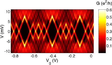
Differential conductance in both the linear and nonlinear response regimes is shown in Fig. 2, which clearly reveals the blockade regions (the black diamonds) and discrete electronic structure. Figure 1 can be thus considered as a cross-section of Fig. 2 along the line corresponding to . The three large diamonds in Fig. 2 correspond to the plateaus between the successive four-peak patterns from Fig. 1. The smaller diamonds, in turn, correspond to the blockade regions between the peaks inside the corresponding four-peak sequence.
The Fano factor, calculated as a function of the gate voltage and for the same parameters as in Fig. 1, is shown in Fig. 3 for several values of the bias voltage, . The latter condition ensures that the shot noise dominates over the thermal Nyquist-Johnson noise. blanterPR00 When , the contribution to the noise due to thermal fluctuations is significant, and in the strictly linear response regime, , the corresponding Fano factor diverges due to nonzero thermal noise and vanishing of the average current density. Let us look first at the gate voltage dependence of the Fano factor for the lowest bias voltage shown in Fig. 3, mV. The Fano factor fluctuates then between values corresponding to the sub- and super-Poissonian noise. The super-Poissonian shot noise () occurs in the blockade regions, whereas the sub-Poissonian shot noise () is observed outside the blockade regions, where the sequential transport is energetically allowed. The minima in Fig. 3 correspond then to positions of the peaks in Fig. 1, and vice versa the maxima in Fig. 3 correspond to the regions between the peaks in Fig. 1. It is noteworthy that this type of correlation strongly resembles that reported for a zero-dimensional conventional (InAs) quantum dots. nauen
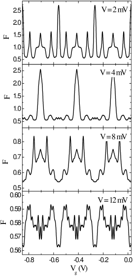
When the bias voltage increases (see Fig. 3 for mV), the shot noise becomes sub-Poissonian, except for those gate voltage regions, where sequential transport is still suppressed. This takes place only for gate voltages around the centers of the large diamonds from Fig. 2. When the bias voltage increases further (see the curves for mV and mV in Fig. 3), the system is beyond the blockade regime independently of the gate voltage. The corresponding Fano factor is always smaller than unity, although it fluctuates with increasing the gate voltage. The suppression of the Fano factor below in the sequential transport regime is a consequence of the Coulomb and exchange correlations in electronic transport. This behavior is different from that observed in the blockade regime, where . onac06 However, one should bear in mind that the sequential transport is negligible in the blockade regions and the current is dominated there by higher-order (e.g. cotunneling) contributions. Thus, the Fano factor in the blockade regions may be significantly modified (in particular reduced) by the cotunneling current. This, however, is beyond the scope of this paper, in which the considerations are limited to the first-order tunneling processes.
The bias dependence of the Fano factor is explicitly shown in Fig. 4 for two different values of the gate voltage. The first value (left column in Fig. 4), V, corresponds to the center of the small diamond shown in Fig. 2, whereas the second value (right column in Fig. 4), V, corresponds to the center of the large diamond. In order to see a clear correlation with transport properties, the current and differential conductance are also shown there. Firstly, the regions where the current is suppressed are clearly visible, while for voltages above the threshold voltage electrons tunnel one by one through the system giving rise to the current, see Figs. 4a and d. Secondly, by increasing the bias voltage, one increases the number of nanotube charge states participating in transport. This leads to a number of peaks in the differential conductance, which can be seen in Figs. 4b and e. On the other hand, the corresponding Fano factor is displayed in Figs. 4c and f. As already mentioned above, the Fano factor diverges in the limit of zero bias due to thermal noise. When , the shot noise becomes dominant, and the Fano factor is then significantly reduced. However, it is still super-Poissonian in the regions, where the current is exponentially suppressed (blocked either by the charging energy or by the absence of discrete levels available for tunneling in the tunneling window). The factor becomes significantly reduced below the Schottky value, , for the bias voltages large enough to set the system beyond the blockade regions. The corresponding Fano factor is then slightly above 0.5, which clearly shows suppression of the shot noise in comparison to the Poissonian transport processes, and also indicates the important role of Coulomb correlations in transport.


The super-Poissonian shot noise in the Coulomb blockade regime is particularly pronounced close to the threshold voltage above which the sequential transport is allowed, see Fig. 4c and f. This enhancement can be accounted for as follows. Assume that the voltage is slightly below the threshold one (close to the maximum of the peak in the Fano factor). The system is then in the blockade regime, where the current is exponentially suppressed. A nonzero small current can flow due to thermal excitations. There is an exponentially small probability that one electron leaves the CNT (reducing its charge state) and then another electron tunnels to the CNT, either to the same energy level or to a level of higher energy. If it tunnels to the level of higher energy, transport through this level is allowed and the electron can easily leave the nanotube, while another one can jump to the same level or to the level of lower energy. If it tunnels to the same level, further tunneling processes are allowed. If it tunnels to the low energy level, the system becomes blocked again. Similar scenario also holds when an electron tunnels first to the CNT (increasing its charge state) and then leaves the CNT. All this leads to large fluctuations in the current, and consequently to super-Poissonian shot noise. However, as we have already mentioned above, the sequential transport is negligible in the blockade regions and the current is dominated there by higher-order (e.g. cotunneling) contributions (not considered here). Thus, the Fano factor in the blockade regions may be significantly modified (reduced) by the cotunneling current.

We also notice that experimentally one usually measures the excess noise, . The corresponding Fano factor is then defined as, . In Fig. 5 we show the bias voltage dependence of the Fano factor for V, calculated using the total shot noise, , and calculated using the excess noise, . One can see that in the sequential tunneling regime the two definitions yield equal Fano factors, . This is due to the fact that the noise due to sequential tunneling in the Coulomb blockade regime is negligible as compared to the noise above the threshold voltage, . Interestingly, the super-Poissonian behavior observed in the Coulomb blockade is also present irrespective of the definition of the Fano factor. The only difference between and can be seen in the low bias voltage regime where and , as , see Fig. 5. Therefore, in this paper we only show and discuss the Fano factor calculated from the total shot noise, , while we notice that the behavior of exactly reflects the behavior of , except for .
IV Carbon nanotubes coupled to ferromagnetic leads
Carbon nanotubes connected to ferromagnetic leads are of particular importance for modern magnetoelectronics. cottet06 ; schonenberger06 It is worth noting that the magneto-electronics based on all-metal multilayers has been making impressive progress over the last two decades. Owing to the discovery of the giant and tunnel magnetoresistance effects, the multilayer-based devices are now wide-spread in the modern electronics (nonvolatile memory elements, angular meters, read/write heads, etc.). Intensive studies have also been carried out on all-semiconductor magnetic systems, since the discovery of ferromagnetic semiconductors. ohno The hybrid systems consisting of ferromagnetic metals or semiconductors and moleculessanvito06 ; naber open a new area in modern magnetoelectronics, and therefore draw attention of physicists, engineers and technologists. A very promising example of magnetic metal/molecule junctions are ferromagnetically contacted CNTs, studied in this section.
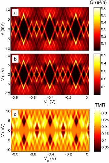
We consider thus electronic transport in the situation when the CNT is weakly coupled to two ferromagnetic leads. The charge current depends then on magnetic configuration of the system, i.e. on the relative alignment of the leads’ magnetic moments. Differential conductance in the parallel and antiparallel magnetic configurations as a function of the bias and gate voltages is shown in Fig. 6a and b. As one can note from the corresponding scales, the conductance is smaller in the antiparallel configuration. This is a general behavior, characteristic of the so-called normal spin valves (normal spin valve effect), and results from the spin asymmetry in tunneling processes. Apart from this difference, the general behavior of differential conductance with transport and gate voltages in both configurations is qualitatively similar, with characteristic diamonds corresponding to blockade regions and four-fold periodicity in the linear response regime (similar to those found in CNTs contacted to nonmagnetic leads, see Fig. 2).
A quantity which takes into account the difference between Fig. 6a and b, and which is of practical importance, is the so-called tunnel magnetoresistance (TMR). The TMR phenomenon consists in a change of the tunneling current when magnetic configuration varies from antiparallel to parallel alignment, and is quantitatively defined as julliere75 ; barnas98
| (8) |
where () is the current flowing through the biased system in the parallel (antiparallel) magnetic configuration. The dependence of TMR on the transport and gate voltages is shown in Fig. 6c. From this plot one can conclude that TMR in the strictly linear response regime () is constant, i.e. independent of the gate voltage. More precisely, it is equal to a half of the Julliere value julliere75 for the corresponding planar junction, i.e. . This behavior is rather general for electronic transport through quantum dots when only first-order transport processes are taken into account, and holds no longer when higher-order processes are included – especially in the blockade regions. weymannPRB05 We note again, that including higher-order contributions may significantly change the TMR in the blockade regions, i.e. in the areas of Fig. 6c corresponding to the black diamonds in Fig. 6a and b. Generally, one may expect some enhancement of TMR in these regions, similarly to the enhancement of TMR due to cotunneling processes, observed in other magnetic tunnel junctions including also granular structures.
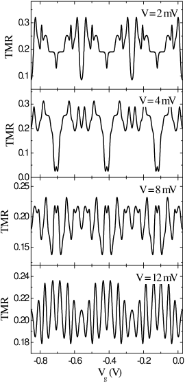
As follows from Fig. 6c, TMR is no longer constant in the nonlinear transport regime. This is shown explicitly in Fig. 7, where the gate voltage dependence of TMR is presented for several values of the bias voltage. The TMR is always positive for the assumed values of the parameters, and oscillates with the gate voltage (contrary to the linear response regime, where TMR is constant). The amplitude of the oscillations, however, decreases with increasing the bias voltage.
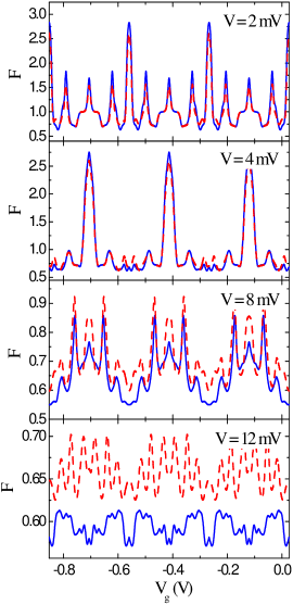
The gate voltage dependence of the Fano factor in the parallel and antiparallel magnetic configurations is shown in Fig. 8 for a few values of the bias voltage. The general features of the Fano factor with increasing bias and gate voltages are similar to those observed in the case of CNTs contacted to nonmagnetic electrodes. As before, the noise is super-Poissonian in the blockade regions, and sub-Poissonian outside the blockade regions. However, the Fano factor in the antiparallel configuration is different from that in the parallel one, and may be either larger or smaller than the latter. This difference is particularly pronounced for larger values of the bias voltage, where the system is out of the blockade regions. We note that for the value of the spin polarization of the leads assumed in calculations, the Fano factor in the antiparallel configuration, , is larger than the Fano factor in the parallel configuration, . The ratio of however depends on the spin polarization of the leads, and for half-metallic electrodes becomes super-Poissonian, while approaches unity. This behavior is similar to that observed in quantum dots. bulkaPRB00 ; cottetPRB04 ; weymannJPCM07
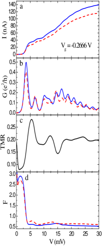
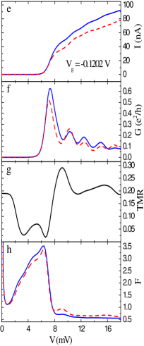
The bias voltage dependence of the Fano factor is shown explicitly in Fig. 9 for two different values of the gate voltage chosen so that the first (second) value corresponds to the middle of the small (large) diamond in Fig. 6. Figure 9 clearly shows that the shot noise is sub-Poissonian, except for the blockade regions, where the noise is enhanced above the Schottky value. This behavior is similar to that observed in CNTs contacted to nonmagnetic leads, and its physical origin is the same as it does not result from magnetism of the electrodes. The effect is only quantitatively modified by ferromagnetism of the electrodes – the magnitude of the super-Poissonian shot noise is different in parallel and antiparallel configurations, as shown in Figs. 8 and 9. In addition, in Figs. 9a and e we also show the current flowing through the system in both magnetic configurations. The difference in currents, resulting from spin asymmetry in tunneling processes in the antiparallel configuration, leads to nonzero TMR displayed in Figs. 9c and g. On the other hand, the bias dependence of the differential conductance displays characteristic peaks, indicating the different charge states of the nanotube being active in transport, see Figs. 9b and f.
V Summary and conclusions
Using the real-time diagrammatic approach we have analyzed transport through CNTs contacted to nonmagnetic and also ferromagnetic electrodes in the weak coupling regime, where the effects due to charging of CNT with individual electrons are clearly seen in transport characteristics. Numerical results on the conductance in linear response regime reproduce quite well the experimentally observed four-peak patterns. Generally, conductance in both the linear and nonlinear transport regimes reveals features of the discrete electronic structure of the CNT-based quantum dots. When the CNT is contacted to ferromagnetic leads, the difference in conductance in the parallel and antiparallel configurations leads to TMR, which also reveals characteristic features of the discrete charging with single electrons and discrete intrinsic electronic structure of the CNTs.
We have also found that in the sequential tunneling regime the shot noise of the single wall metallic carbon nanotubes is generally suppressed below the Schottky value, except for the blockade regions, where it is larger than the Schottky value. For voltages above the threshold for sequential tunneling the corresponding Fano factor has been found to be slightly above 0.5, while in the blockade regions it is larger than 1. However, we expect that the shot noise in the blockade regions will be strongly modified by higher-order contributions to the current. It has also been shown that for the assumed parameters the Fano factor in the antiparallel configuration is typically larger than the Fano factor in the parallel configuration.
Acknowledgements.
This work was supported by: the EU grant CARDEQ under contract IST-021285-2, and the Polish Ministry of Science and Higher Education as a research project in years 2006-2009. I.W. also acknowledges support from the Foundation for Polish Science.References
- (1) L. P. Kouwenhoven, D. G. Austing and S. Tarucha, Rep. Prog. Phys. 64, 701 (2001).
- (2) P. Harrison, Quantum Wells, Wires, and Dots: Theoretical and Computational Physics (Wiley, Chichester, 1999).
- (3) S. A. Wolf, D. D. Awschalom, R. A. Buhrman, J. M. Daughton, S. von Molnar, M. L. Roukes, A. Y. Chtchelka, and D. M. Treger, Science 294, 1488 (2001).
- (4) Semiconductor Spintronics and Quantum Computation, ed. by D. D. Awschalom, D. Loss, and N. Samarth (Springer, Berlin 2002).
- (5) S. Maekawa and T. Shinjo, Spin Dependent Transport in Magnetic Nanostructures (Taylor & Francis 2002).
- (6) I. Zutic, J. Fabian, S. Das Sarma, Rev. Mod. Phys. 76, 323 (2004).
- (7) S. Sanvito and A. R. Rocha, J. Comput. Theor. Nanos. 3, 624 (2006).
- (8) S. Maekawa, Concepts in Spin Electronics (Oxford 2006).
- (9) R. Saito, M. S. Dresselhaus, and G. Dresselhaus, Physical Properties of Carbon Nanotubes (London, UK: Imperial College Press, 1998).
- (10) M. P. Anantram and F. Leonard, Rep. Prog. Phys 69, 507 (2006).
- (11) W. Hoenlein, G. S. Duesberg, A. P. Graham, F. Kreupl, M. Liebau, W. Pamler, R. Seidel, and E. Unger, Microelectron. Eng. 83, 619 (2006).
- (12) K. Tsukagoshi, B. W. Alphenaar, and H. Ago, Nature 401, 572 (1999).
- (13) B. Zhao, I. Mönch, H. Vinzelberg, T. Mühl, and C. M. Schneider, Appl. Phys. Lett. 80, 3144 (2002); J. Appl. Phys. 91, 7026 (2002).
- (14) Jae-Ryoung Kim, Hye Mi So, Ju-Jin Kim, Jinhee Kim, Phys. Rev. B 66, 233401 (2002).
- (15) S. Sahoo, T. Kontos, J. Furer, C. Hoffmann, M. Gräber, A. Cottet, and C. Schönenberger, Nature Physics 1, 102 (2005).
- (16) A. Jensen, J. R. Hauptmann, J. Nygard, and P. E. Lindelof, Phys. Rev. B 72, 035419 (2005).
- (17) H. T. Man, I. J. W. Wever, and A. F. Morpurgo, Phys. Rev. B 73, 241401(R) (2006)
- (18) L. W. Liu, J. H. Fang, L. Lu, H. F. Yang, A. Z. Jin, and C. Z. Gu Phys. Rev. B 74, 245429 (2006).
- (19) B. Nagabhirava, T. Bansal, G. U. Sumanasekera, and B. W. Alphenaara, L. Liu, Appl. Phys. Lett. 88, 023503 (2006)
- (20) S. Krompiewski, phys. stat. sol. (b) 242, 226 (2005).
- (21) S. Krompiewski, Semicond. Sci. Technol. 21, S96 (2006).
- (22) A. Cottet and M-S. Choi, Phys. Rev. B 74, 235316 (2006).
- (23) A. Cottet, T. Kontos, S. Sahoo, H. T. Man, M.-S. Choi, W. Belzig, C. Bruder, A. F. Morpurgo, and C. Sch nenberger, Semicond. Sci. Technol. 21, S78 (2006).
- (24) C. Schönenberger, Semicond. Sci. Technol. 21, S1 (2006).
- (25) W. Liang, M. Bockrath, and H. Park, Phys. Rev. Lett. 88, 126801 (2002).
- (26) S. Sapmaz, P. Jarillo-Herrero, J. Kong, C. Dekker, L. P. Kouwenhoven, and H. S. J. van der Zant, Phys. Rev. B 71, 153402 (2005).
- (27) Y. Oreg, K. Byczuk, and B. I. Halperin, Phys. Rev. Lett. 85, 365 (2000).
- (28) R. Egger and A. O. Gogolin, Phys. Rev. Lett. 79, 5082 (1997); Eur. Phys. J. B 3, 281 (1998).
- (29) C. Kane, L. Balents and M. P. A. Fisher, Phys. Rev. Lett. 79, 5086 (1997).
- (30) M. Bockrath, D. H. Cobden, J. Lu, A. G. Rinzler, R. E. Smalley, L. Balents and P. L. McEuen, Nature 397, 598 (1999).
- (31) L. Mayrhofer and M. Grifoni, Phys. Rev. B 74, 121403 (2006).
- (32) L. Mayrhofer and M. Grifoni, Eur. Phys. J. B 56, 107 (2007).
- (33) S. Koller, L. Mayrhofer, M. Grifoni, W. Wetzels, cond-mat/0703756 (unpublished).
- (34) E. Onac, F. Balestro, B. Trauzettel, C. F. J. Lodewijk, and L. P. Kouwenhoven, Phys. Rev. Lett. 96, 026803 (2006).
- (35) F. Wu, P. Queipo, T. Tsuneta, T. H. Wang, E. Kauppinen, and P. J. Hakonen, cond-mat/0702332 (unpublished).
- (36) T. Tsuneta, P. Virtanen, F. Wu, T. Wang, T. T. Heikkilä, and P. J. Hakonen, cond-mat/0706.2658 (unpublished).
- (37) D. V. Averin and A. A. Odintsov, Phys. Lett. A 140, 251 (1989); D. V. Averin and Yu. V. Nazarov, Phys. Rev. Lett. 65, 2446 (1990); K. Kang and B. I. Min, Phys. Rev. B 55, 15412 (1997).
- (38) I. Weymann and J. Barnaś, Phys. Rev. B 75, 155308 (2007).
- (39) I. Weymann, J. König, J. Martinek, J. Barnaś, and G. Schön, Phys. Rev. B 72, 115334 (2005).
- (40) H. Schoeller and G. Schön, Phys. Rev. B 50, 18436 (1994); J. König, J. Schmid, H. Schoeller, and G. Schön, Phys. Rev. B 54, 16820 (1996).
- (41) A. Thielmann, M. H. Hettler, J. König, and G. Schön, Phys. Rev. B 68, 115105 (2003); Phys. Rev. B 71 045341 (2005).
- (42) Ya. M. Blanter and M. Büttiker, Phys. Rep. 336, 1 (2000).
- (43) A. Nauen, F. Hohls, N. Maire, K. Pierz, and R. J. Haug , Phys. Rev. B 70, 033305 (2004).
- (44) H. Ohno, D. Chiba, F. Matsukura, T. Omiya, E. Abe, T. Dietl, Y. Ohno, and K. Ohtani, Nature 408, 946 (2000).
- (45) W. J. M. Naber, S. Faez and W. G. van der Wiel, cond-mat/0703455 (unpublished).
- (46) M. Julliere, Phys. Lett. A 54, 225 (1975).
- (47) J. Barnaś and A. Fert, Phys. Rev. Lett. 80, 1058 (1998).
- (48) B. R. Bułka, Phys. Rev. B 62, 1186 (2000).
- (49) A. Cottet, W. Belzig and C. Bruder, Phys. Rev. B 70, 115315 (2004).
- (50) I. Weymann and J. Barnaś, J. Phys.: Condens. Matter 19, 096208 (2007).