Terahertz conductivity of localized photoinduced carriers in Mott insulator YTiO3 at low excitation density, contrasted with metallic nature in band semiconductor Si
Abstract
We performed optical-pump terahertz-probe measurements of a Mott insulator YTiO3 and a band semiconductor Si using a laser diode (1.47 eV) and a femtosecond pulse laser (1.55 eV). Both samples possess long energy-relaxation times (1.5 ms for YTiO3 and 15 s for Si); therefore, it is possible to extract terahertz complex conductivities of photoinduced carriers under equilibrium. We observed highly contrasting behavior - Drude conductivity in Si and localized conductivity possibly obeying the Jonscher law in YTiO3. The carrier number at the highest carrier-concentration layer in YTiO3 is estimated to be 0.015 per Ti site. Anisotropic conductivity of YTiO3 is determined. Our study indicates that localized carriers might play an important role in the incipient formation of photoinduced metallic phases in Mott insulators. In addition, this study shows that the transfer-matrix method is effective for extracting an optical constant of a sample with a spatially inhomogeneous carrier distribution.
pacs:
78.47.+p, 72.80.Ga, 71.30.+h1 Introduction
Recent discoveries of photoinduced metallic phases in several Mott insulators[1, 2, 3, 4, 5, 6] made us consider the strongly correlated electron physics from a new point of view. However, the optical properties of photoinduced carriers in Mott insulators are not well understood even at low excitation densities. Understanding these optical properties is a prerequisite to understanding the incipient creation of metallic phases. Drude response by itinerant carriers is observed in the case of band semiconductors with low excited-carrier density (10141016 cm-3)[7, 8, 9, 10]. The comparison between the optical properties of photoinduced carriers at low excitation densities in Mott insulators and those in band semiconductors would be important in gaining deeper insight into strongly correlated electron physics.
The detailed nature of various carrier conductions, exhibiting Drude or hopping conduction, can be well characterized in the terahertz (THz) regime[11, 12, 13, 14]. THz time-domain spectroscopy (THz-TDS) is a powerful tool for analysing terahertz conductivity (). The remarkable advantage of THz-TDS is its simultaneous determination of both the real and imaginary parts of , without using the Kramers-Kronig transformation[15]. The coherent nature of the THz pulse is also utilized to investigate photoinduced by, for instance, optical-pump THz-probe (OPTP) studies. Recent progress in THz technologies[16, 17] and the methodology of analysis[18, 19, 20] in OPTP experiments enable evaluation of transient in many substances, such as semiconductors, high-Tc superconductors, liquids and organic materials[8, 21, 22, 23, 24, 25, 26, 27, 28, 29, 30, 31].
Because the OPTP method essentially detects non-equilibrium processes, such as surface recombination and carrier diffusion, the time dependence of a complicated spatial carrier distribution must be considered[8, 32]. This difficulty is avoided by using thin-film samples[21, 22, 23, 24, 28, 31] where the optical pump pulse penetrates, and by analysing the photoinduced phase as a layer with a homogeneous [8, 22, 24, 28, 33]. Furthermore the extraction of , varying quickly compared with the pulse width of THz probe pulse, only seems possible within some restricted conditions[18, 19, 20]. Therefore, to analyse photoinduced for a wide variety of Mott insulators, free from the restrictions in sample preparation and analysis, we initially examined a nearly equilibrium state of photoexcited bulk material with a longer energy-relaxation time, . The photoexcitation of a material with longer creates a quasi-equilibrium state averaging over various non-equilibrium processes, making it easy to obtain the optical constants of the highest carrier-concentration region in the material.
Our analysis also required extracting of materials with inhomogeneous carrier distributions in a more rigorous manner. One good candidate for accomplishing this is the transfer-matrix method, which expresses inhomogeneous carrier distribution by a multi-layer system. This method has been briefly commented on in the literature[8]. The promise that the transfer-matrix method can incorporate inhomogeneity is seen in the analyses of reflectivity in optical pump-probe studies[34, 35]. Although it is a versatile method, its effectiveness has not been thoroughly discussed, especially in THz-TDS studies.
In this study, we found that of a Mott insulator YTiO3 with Mott gap of approximately 1 eV[36] is 1.5 ms at 1.47 eV photoexcitation. We characterized the photoinduced by comparing it with that of a band semiconductor Si with a bandgap of 1.1 eV[37]. We also present a more detailed discussion of the transfer-matrix method.
2 Experimental method
Single-crystalline samples of YTiO3, with the orthorhombic perovskite GdFeO3-type structure, were grown by the floating zone method[38]. The Si sample was commercial high-resistivity Si.
Photoconductivity was measured to assess . The light emitted from a multimode continuous wave (CW) laser diode (LD) with photon energy of 1.47 eV was modulated and used for illuminating the sample under an electric field of about 0.3 kV/cm. The photocurrent flowing through a 100 resistance, connected in series with the sample, was lock-in detected.
OPTP experiment was performed by a transmission THz-TDS system described in detail elsewhere[39, 40]. The thicknesses of platelet samples are 420 m for YTiO3 and 512 m for Si. The optical pulses were generated by a mode-locked Ti-sapphire laser with a repetition rate of 76 MHz and central wavelength of 800 nm. Both the THz emitter and detector were low-temperature grown GaAs photoconductive antennas. Si lenses were attached to the antennas to enhance the emission power and collection efficiency of THz pulses. The THz spectral range in this experiment was between 0.5 and 8 meV. The THz-wave-emission sides of the samples were photoexcited by the multi-mode CW LD with an incident angle of 45∘. The pump-beam power was 0.8 W for Si and 1.2 W for YTiO3. For YTiO3, the polarization of THz electric field is parallel to the b-axis. The beam diameter of the LD light was about 8 mm and larger than that of the THz probe pulse, which is energy dependent (e.g. 2 mm at 2 meV and 1 mm at 4 meV). The fluence rate was 1.6 W/cm2 for Si and 2.4 W/cm2 for YTiO3, respectively. The temperature rise resulting from the thermalisation by photoexcitation[41] is estimated not to exceed 1 K.
OPTP measurements were also performed with the 1.55 eV optical-pump pulses split from the Ti-sapphire laser to investigate the nature of conduction of carriers induced by light with photon energy larger than that of the CW LD. This experiment studied the anisotropy of photoinduced in YTiO3. The optical-pump pulse power was 230 mW. The optical-pump pulse beam diameter was about 2 mm (fluence: 96 nJ/cm2) - slightly smaller than that of the THz probe pulse below 2 meV. The was applied along either the - or -axis, maintaining the polarization of the optical-pump pulse electric field parallel to the - or -axis.
All measurements were performed at room temperature.
3 Results and Discussion
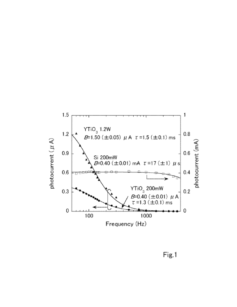
Figure 1 shows the modulation-frequency dependence of . Increasing the modulation frequency causes to decrease, according to , where is the proportional coefficient. The obtained and are listed in the figure. Longer ( 15 s for Si and 1.5 ms for YTiO3) indicates that the samples are in quasi-equilibrium photoinduced state during the THz-TDS measurements. of YTiO3 is almost excitation-intensity independent; this implies that a thermal effect does not dominate the relaxation process. Although the direction of and of electric field of the CW LD pump are not identified accurately in YTiO3, a huge anisotropic that depends on the direction of and the polarization of the excitation light is not anticipated. The OPTP results shown later support this (see Fig. 7).
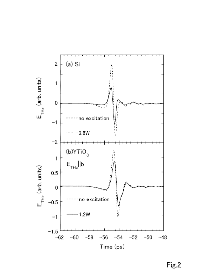
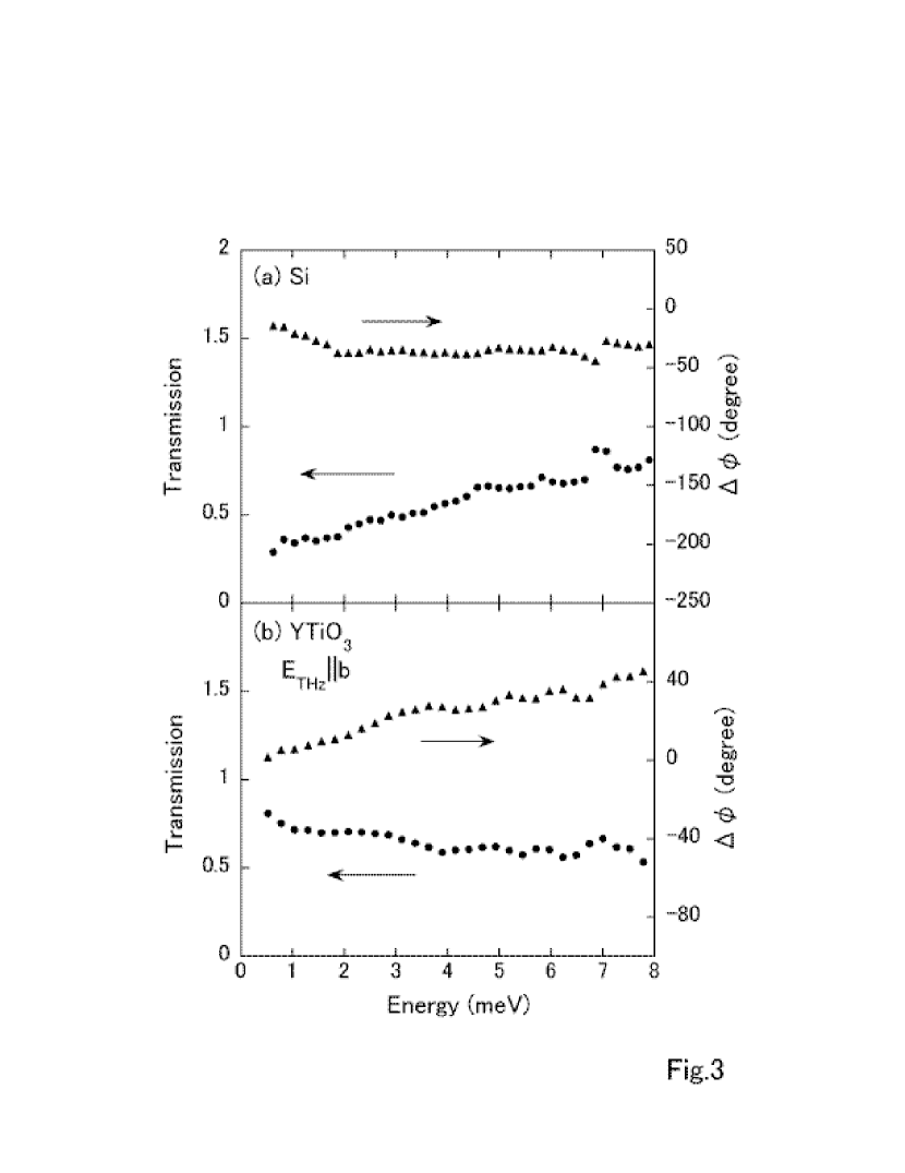
The temporal evolution of transmitted through Si and YTiO3 are shown in Fig. 2(a) and 2(b), respectively, with and without LD excitations (1.47 eV). Photoexcitation attenuates both THz waves implying THz wave absorption is by the photoinduced carriers. THz energy dependence of transmission and phase shift are obtained by Fourier transformation of THz waves, as shown in Fig. 3(a) and 3(b). They are calculated with the equations and , where and are the Fourier transformed amplitude and phase, with and without excitation, respectively. THz wave absorption by photoinduced carriers is responsible for decreasing below 1 for both samples, but the two exhibit different energy dependencies. As the THz energy increases, of Si approaches 1, while that of YTiO3 gradually decreases. The opposite sign of of the two samples strongly indicates different fundamental conduction mechanisms of the photoinduced carriers. Negative (positive) roughly means the refractive index is reduced (increased), compared with an unexcited state, which influences the negative (positive) real part of the dielectric constant of photoinduced carriers. As explained below, these results indicate a metallic nature below a plasma frequency in Si, and a localized nature, such as hopping carriers, in YTiO3.
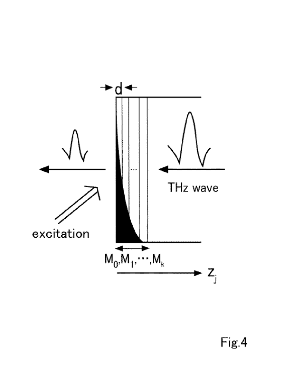
Before showing the photoinduced of Si and YTiO3, we mention the detailed procedure of the transfer-matrix method. A spatially inhomogeneous distribution of photoinduced carriers is initially regarded as exponentially decaying. Subsequently a non-exponentially decaying distribution is introduced. The photoinduced phase with an exponentially decaying carrier distribution is divided into many thin slabs (see Fig. 4). Each slab is supposed to have a uniform complex refractive index whose value is set to reproduce the exponential decay of the photoinduced carrier concentration. The transfer-matrix of each slab is described by
| (1) |
where is the number index of the slab, , is the incident THz wavelength in vacuum, and is the slab thickness[42, 43]. The of each slab is calculated from the complex dielectric constant using,
| (2) |
where is without excitation, , the parameter to be optimized in this analysis, is resulting from carriers at the photoexcited surface of the sample, () is the depth from the photoexcited surface into the sample along the THz wave propagation, and is the optical penetration depth. For Si, frequency independent [44] of 11.7 is used. For YTiO3, is experimentally determined by the THz-TDS measurement and is weakly energy dependent (e.g. 16.5+0.4 at 2 meV and 17+0.4 at 4 meV). of Si at 1.47 eV is determined to be 8.4 m using the absorption coefficient from an optical data handbook[45]. That of YTiO3 at 1.47 eV was calculated to be 0.22 m from the reported reflectivity spectra[46] (0.05-40 eV) combined with the Kramers-Kronig transformation. Then the total matrix is described as
| (3) |
where is the total number of photoexcited slabs. Finally, the THz complex transmission is given by
| (4) |
where and mean the THz wave transmission with and without excitation, respectively, and . The fitting of experimental and following the above mentioned procedure provides resulting from carriers at the photoexcited surface through
| (5) |
where is the vacuum permittivity. Note that the convergence of transmission is checked carefully by decreasing the thickness or by increasing the number of slabs. A thickness of the photoexcited phase (, =100) 5 to 10 times thicker than is typically employed.
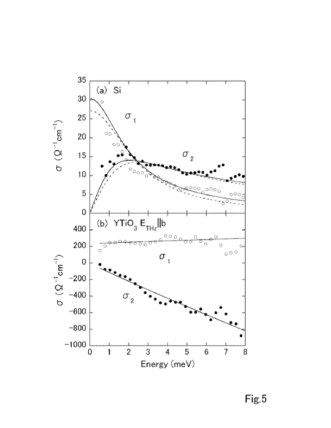
Figure 5 shows photoinduced of Si and YTiO3. of Si can be interpreted by the Drude model as
| (6) | |||||
| (7) |
where is the carrier density, is the mobility, is the carrier collision rate and is the effective mass. The photoexcitation introduces both electrons and holes; therefore, the tentatively assigned value is 0.26 for electrons and 0.37 for holes[44], where is the free-electron mass. Hereafter, of each carrier is denoted as for electrons and for holes. We have considered the following two cases, neither of which can be excluded at the present stage. One is the two-carrier model of electrons and holes. The other takes only electrons into consideration, assuming that holes with heavy do not contribute to . The solid lines in Fig. 5(a) represent the calculated for the two-carrier model and the broken lines represent the electron-only model. The curves are in agreement with the experimental . This suggests that the itinerant carriers are certainly photogenerated in Si. The obtained and are 2410 (210) cm2/Vs and 500 (90) cm2/Vs for the two-carrier model, and is 1820 (100) cm2/Vs for the other model. They are roughly consistent with the literature values[37], but it is to be noted that in both models might be larger than the predicted ones. The ambiguity of may be responsible for this deviation.
The most striking feature in of YTiO3 is the negative . It suggests an existence of localized carriers[27, 39, 47], which is very different from Si. The localization may arise from the on-site strong Coulomb interaction between 3d electrons in YTiO3. To explain , we used the empirical Jonscher law[48], which expresses of many materials with hopping carriers. The Jonscher law is given by[48, 49]
| (8) | |||||
| (9) |
where is the DC conductivity, the proportional coefficient and is restricted between 0 and 1. As shown in Fig. 5(b), the solid curves from the Jonscher law seem to agree with experimental . In the solid curves, , and are 0.95, 235 (10) cm-1 and 2.40 (0.05)10-11 cm-1s0.95, respectively. The allowed ranges from 0.91 to 0.99, and corresponding and are 210 (10) cm-1 and 1.41 (0.03)10-10 cm-1s0.91, and 260 (10) cm-1 and 1.43 (0.03)10-12 cm-1s0.99, respectively.
Note that can be also fitted by a two-component model, such as the Drude-Lorentz. The estimated photoinduced carrier number at the surface layer is about 0.015 per Ti site. Photoexcited YTiO3 with the derived carrier density would be equivalent to chemically hole-doped Y1-xCaxTiO3 with much less than 0.1 given in Ref. 36. The spectrum of Y1-xCaxTiO3 in this composition region is very different than a Drude response. Therefore, it would be difficult to expect a Drude component to exist. Clarifying this point might require broadband spectroscopic information obtained under photoexcitation or the temperature dependence of .
Since long relaxation times, , are observed in both samples, a diffusion or a surface-recombination process, making the carrier distribution a non-exponential decay type, must be considered, and the analysis method modified. The carrier number along the THz wave propagation in a quasi-equilibrium state is obtained using a one-dimensional diffusion equation[50] as follows:
| (10) |
where depends on the time and the position along the THz wave propagation, and is the -function. is the diffusion coefficient and given by
| (11) |
where is equal to , is the Boltzmann constant and is the sample temperature equal to 300 K. The solution[50] of eq. (10) is
| (12) | |||||
where is the surface recombination velocity and is related to the error function by erf. The carrier number in the quasi-equilibrium state requires the integration of with respect to ,
| (13) |
Therefore, with the assumption of a conduction model and the knowledge of determined by appropriate and , can be calculated using eq. (4). In this case, eq. (2) is replaced by
| (14) |
where and are and of the highest carrier-concentration layer, respectively.
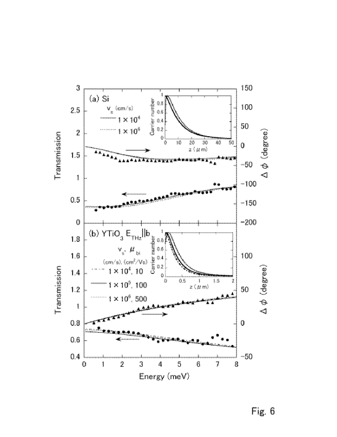
After the determination of of Si (= 346 cm2/Vs) using the literature values[37], is varied between 1104 cm/s and 1106 cm/s. Representative normalized at are shown in the inset of Fig. 6(a). The is observed around 12 m. Assuming that both electrons and holes obeying the Drude conductivity are responsible for , is confirmed as being consistent with experimental data for both (see Fig. 6(a)). The estimated is 5.2 (0.3)1016 cm-3 and is comparable to that obtained by the previous model. This indicates that, at the highest carrier-concentration layer almost the same can be obtained, irrespective of the carrier distribution decay type. For YTiO3, both and are unknown parameters. The wide range sweep of and gives various curves as depicted in the inset of Fig. 6(b) with peak positions around 0.1 m. For each , the experimental is well reproduced by the Jonscher law, where is restricted within the same range obtained in Fig. 5(b) (0.910.99). Typical examples are shown in Fig. 6(b) with of 0.95. The other parameters ( in cm-1 and in cm-1s0.95) for the dotted-solid, solid and broken lines are 125(10) and 1.40(0.05)10-11, 125(10) and 1.2(0.1)10-11, and 90(10) and 1.0(0.1)10-11, respectively. and calculated from the parameters are half to two-thirds of those in Fig. 5(b). Thus, for YTiO3, the extracted from the model with exponentially-decaying carrier distribution roughly represents the highest carrier-concentration layer in the model using eq. (14).
The photoinduced carrier number at the highest carrier-concentration layer in YTiO3 is calculated as 0.015 per Ti site[51]. It can be proposed, therefore, that a phase with localized carriers would emerge initially at the photogeneration of the metallic phase in Mott insulators. Photoexcitation creates both electrons and holes, which differs from chemical doping, and a comparison of between photoexcited YTiO3 and a hole-doped Y1-xCaxTiO3 is discussed. The absolute value of of photoexcited state might be much larger than that of corresponding Y1-xCaxTiO3 if the extrapolation of in Y1-xCaxTiO3 is carried out toward the THz energy. The preservation of spectral weight implies that the localization energy of photoinduced carriers would be much lower than for holes in Y1-xCaxTiO3, even if both holes and electrons contribute to in photoexcited YTiO3. As it is not clear that the large difference in localization energy originates from only holes in such a low-carrier system, it is plausible that electrons with small localization energies also contribute to . Therefore of photoexcited YTiO3 would be supported by bound electrons as well as holes.
In a halogen-bridged Ni one-dimensional chain compound [Ni(chxn)2Br]Br2 (chxn = cyclohexanediamine), which is compared with YTiO3 composed of a three-dimensional Ti network, the localized is determined at a lower excitation density[3]. Despite being in a different energy region, carrier localization in photoexcited Mott insulators at low excitation densities may be the general phenomenon, irrespective of the dimensionality.
The fact that one-dimensional Mott insulators, such as [Ni(chxn)2Br]Br2[3] and Sr2CuO3[52], exhibit in the order of pico-seconds may suggest that dimensionality is a decisive factor of .
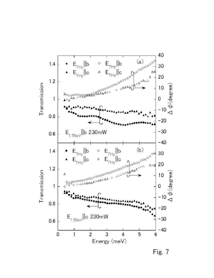
Figure 7 shows and obtained by OPTP experiments using a femtosecond-pulse laser (1.55 eV) for YTiO3. Since the period of optical-pump arrival time (13 ns) is much shorter than , the photoinduced carriers are also in quasi-equilibrium state. In both polarizations of , it is found that the degree of variation from the unexcited state in THz wave amplitude and phase is larger for within the measured THz energy range. This implies that the absolute values of and for are larger than those for . The anisotropy would reflect the crystal symmetry of YTiO3 or the 3-orbital state at Ti site. Comparing with the OPTP results to those using the CW LD, the does not seem to depend strongly on the optical-photon energy.
4 Summary
We have optically characterized photoinduced carriers of Mott insulator YTiO3 at low excitation densities in the THz regime by OPTP measurements, and compared the experimental results with those for band semiconductor Si. The of the photoinduced carriers in YTiO3 is about 1.5 ms. The inhomogeneous carrier distribution along the THz wave propagation can be treated accurately using the transfer-matrix method. This method successfully determined of the highest carrier-concentration layer under the quasi-equilibrium states. YTiO3 shows localized , possibly with the Jonscher law, whereas Si exhibits the Drude response. Anisotropic in YTiO3 is determined. Our study demonstrates that localized carriers might play an important role in the incipient formation of metallic phases in photoexcited Mott insulators. Although the exact origin of the localization in YTiO3 remains an open question, THz-TDS under photoexcitation with another photon energy or for another Mott insulator might provide the answer. We note here that a preliminary THz-TDS experiment of YTiO3 excited by a CW LD of 1.9 eV also leads to localized .
References
References
- [1] K. Miyano, T. Tanaka, Y. Tomioka, and Y. Tokura, Phys. Rev. Lett. 78, 4257 (1997).
- [2] A. Cavalleri, Cs. Tóth, C. W. Siders, J. A. Squier, F. Ráksi, P. Forget, and J. C. Kieffer, Phys. Rev. Lett. 87, 237401 (2001).
- [3] S. Iwai, M. Ono, A. Maeda, H. Matsuzaki, H. Kishida, H. Okamoto, and Y. Tokura, Phys. Rev. Lett. 91, 057401 (2003).
- [4] N. Tajima, J. Fujisawa, N. Naka, T. Ishihara, R. Kato, Y. Nishio, and K. Kajita, J. Phys. Soc. Jpn. 74, 511 (2005).
- [5] M. Chollet, L. Guerin, N. Uchida, S. Fukaya, H. Shimoda, T. Ishikawa, K. Matsuda, T. Hasegawa, A. Ota, H. Yamochi, G. Saito, R. Tazaki, S. Adachi, and S. Koshihara, Science 307, 86 (2005).
- [6] L. Perfetti, P. A. Loukakos, M. Lisowski, U. Bovensiepen, H. Berger, S. Biermann, P. S. Cornaglia, A. Georges, and M. Wolf, Phys. Rev. Lett. 97, 067402 (2006).
- [7] S. E. Ralph, Y. Chen, J. Woodall, and D. McInturff, Phys. Rev. B 54, 5568 (1996).
- [8] M. C. Beard, G. M. Turner, and C. A. Schmuttenmaer, Phys. Rev. B 62, 15764 (2000).
- [9] J. Shan, F. Wang, E. Knoesel, M. Bonn, and T. F. Heinz, Phys. Rev. Lett. 90, 247401 (2003).
- [10] G. L. Dakovski, B. Kubera, S. Lan, and J. Shan, J. Opt. Soc. Am. B 23, 139 (2006).
- [11] M. van Exter and D. Grischkowsky, Appl. Phys. Lett. 56, 1694 (1990).
- [12] N. Katzenellenbogen and D. Grischkowsky, Appl. Phys. Lett. 61, 840 (1992).
- [13] T. -I. Jeon and D. Grischkowsky, Phys. Rev. Lett. 78, 1106 (1997).
- [14] H. Harimochi, J. Kitagawa, M. Ishizaka, Y. Kadoya, M. Yamanishi, S. Matsuishi, and H. Hosono, Phys. Rev. B 70, 193104 (2004).
- [15] G. Grüner, Millimeter and Submillimeter Wave Spectroscopy of Solids (Springer, Berlin, 1998).
- [16] D. Mittleman, Sensing with Terahertz Radiation (Springer, Berlin, 2003).
- [17] K. Sakai, Terahertz Optoelectronics (Springer, Berlin, 2005).
- [18] J. T. Kindt and C. A. Schmuttenmaer, J. Chem. Phys. 110, 8589 (1999).
- [19] H. Němec, F. Kadlec, and P. Kužel, J. Chem. Phys. 117, 8454 (2002).
- [20] H. K. Nienhuys and V. Sundström, Phys. Rev. B 71, 235110 (2005).
- [21] R. D. Averitt, G. Rodriguez, J. L. W. Siders, S. A. Trugman, and A. J. Taylor, J. Opt. Soc. Am. B 17, 327 (2000).
- [22] R. Huber, F. Tauser, A. Brodschelm, M. Bichler, G. Abstreiter, and A. Leitenstorfer, Nature 414, 286 (2001).
- [23] R. D. Averitt, A. I. Lobad, C. Kwon, S. A. Trugman, V. K. Thorsmlle, and A. J. Taylor, Phys. Rev. Lett. 87, 017401 (2001).
- [24] M. C. Beard, G. M. Turner, and C. A. Schmuttenmaer, J. Appl. Phys. 90, 5915 (2001).
- [25] E. Knoesel, M. Bonn, J. Shan, and T. F. Heinz, Phys. Rev. Lett. 86, 340 (2001).
- [26] F. A. Hegmann, R. R. Tykwinski, K. P. H. Lui, J. E. Bullock, and J. E. Anthony, Phys. Rev. Lett. 89, 227403 (2002).
- [27] G. M. Turner, M. C. Beard, and C. A. Schmuttenmaer, J. Phys. Chem. B 106, 11716 (2002).
- [28] J. Demsar, R. D. Averitt, A. J. Taylor, V. V. Kabanov, W. N. Kang, H. J. Kim, E. M. Choi, and S. I. Lee, Phys. Rev. Lett. 91, 267002 (2003).
- [29] R. A. Kaindl, M. A. Carnahan, D. Hägele, R. Lövenlch, and D. S. Chemla, Nature 423, 734 (2003).
- [30] E. Hendry, F. Wang, J. Shan, T. F. Heinz, and M. Bonn, Phys. Rev. B 69, 081101 (2004).
- [31] T. Kampfrath, L. Perfetti, F. Schapper, C. Frischkorn, and M. Wolf, Phys. Rev. Lett. 95, 187403 (2005).
- [32] M. I. Gallant and H. M. van Driel, Phys. Rev. B 26, 2133 (1982).
- [33] M. Schall and P. U. Jepsen, Opt. Lett. 25, 13 (2000).
- [34] H. M. Ma, Y. X. Liu, Y. Fei, and F. M. Li, J. Appl. Phys. 65, 5031 (1989).
- [35] H. Okamoto, Y. Ishige, S. Tanaka, H. Kishida, S. Iwai, and Y. Tokura, Phys. Rev. B 70, 165202 (2004).
- [36] Y. Taguchi, Y. Tokura, T. Arima, and F. Inaba, Phys. Rev. B 48, 511 (1993).
- [37] S. M. Sze, Physics of Semiconductor Devices (Wiley-Interscience, New York, 1981).
- [38] M. Tsubota, F. Iga, T. Nakano, K. Uchihira, S. Kura, M. Takemura, Y. Bando, K. Umeo, T. Takabatake, E. Nishibori, M. Takata, M. Sakata, K. Kato, and Y. Ohishi, J. Phys. Soc. Jpn. 72, 3182 (2003).
- [39] J. Kitagawa, M. Ishizaka, Y. Kadoya, S. Matsuishi, and H. Hosono, J. Phys. Soc. Jpn. 75, 084715 (2006).
- [40] J. Kitagawa, Y. Kadoya, M. Tsubota, F. Iga and T. Takabatake, J. Magn. Magn. Mat. 310 913 (2007).
- [41] The temperature rise under an equilibrium condition is calculated as follows. If all of the excitation power is transformed into heat in a sample, is related to by where is the sample length, is the illuminated area[51] of 0.5 cm2 and is the thermal conductivity of the sample (150 W/mK for Si[37]). With the lack of data for YTiO3, we employ underestimated 10 W/mK.
- [42] M. Born and E. Wolf, Principles of Optics, 6th ed. (Pergamon, New York, 1980).
- [43] H. Harimochi, J. Kitagawa, Y. Kadoya, and M .Yamanishi, Jpn. J. Appl. Phys. 43, 7320 (2004).
- [44] M. van Exter and D. Grischkowsky, Phys. Rev. B 41, 12140 (1990).
- [45] E. D. Palik, Handbook of Optical Constants of Solids (Academic Press, New York, 1985).
- [46] Y. Okimoto, T. Katsufuji, Y. Okada, T. Arima, and Y. Tokura, Phys. Rev. B 51, 9581 (1995).
- [47] D. G. Cooke, A. N. MacDonald, A. Hryciw, J. Wang, Q. Li, A. Meldrum, and F. A. Hegmann, Phys. Rev. B 73, 193311 (2006).
- [48] A. K. Jonscher, Nature (London) 267, 673 (1977).
- [49] S. R. Elliott, Adv. Phys. 36, 135 (1987).
- [50] J. Vaitkus, Phys. Status Solidi A 34, 769 (1976).
- [51] The photoinduced carrier density at is tentatively expressed by where the first term indicates the carrier accumulation resulting from longer at photon energy of 1.47 eV, the second one is the Fresnel loss ( 0.8 for YTiO3 and 0.7 for Si). means the effective defined by / and is equal to 13 m for Si and 0.55 m for YTiO3. This equation is initially applied to the experimental result of Si (Fig. 6(a)) with 5.21016 cm-3, in which is determined to be 0.5 cm2. Using the , the carrier number of YTiO3 can be derived.
- [52] T. Ogasawara, M. Ashida, N. Motoyama, H. Eisaki, S. Uchida, Y. Tokura, H. Ghosh, A. Shukla, S. Mazumdar, and M. Kuwata-Gonokami, Phys. Rev. Lett. 85, 2204 (2000).
