Fermi surface nesting and the origin of Charge Density Waves in metals
Abstract
The concept of a CDW induced by Fermi-surface nesting originated from the Peierls idea of electronic instabilities in purely 1D metals and is now often applied to charge ordering in real low-dimensional materials. The idea is that if Fermi surface contours coincide when shifted along the observed CDW wave vector, then the CDW is considered to be nesting-derived. We show that in most cases this procedure has no predictive power, since Fermi surfaces either do not nest at the right wave vector, or nest more strongly at the wrong vector. We argue that only a tiny fraction, if any, of the observed charge ordering phase transitions are true analogues of the Peierls instability because electronic instabilities are easily destroyed by even small deviations from perfect nesting conditions. Using prototypical CDW materials NbSe2, TaSe2, and CeTe3, we show that such conditions are hardly ever fulfilled, and that the CDW phases are actually structural phase transitions, driven by the concerted action of electronic and ionic subsystems, i.e., q-dependent electron-phonon coupling plays an indispensable part. We also show mathematically that the original Peierls construction is so fragile as to be unlikely to apply to real materials. We argue that no meaningful distinction between a CDW and an incommensurate lattice transition exists.
One common misconception in modern solid state physics is that Fermi surface (FS) nesting is always, or nearly always responsible for a charge density wave (CDW). While many materials experience a structural or magnetic transition with a wave vector that is incommensurate or badly commensurate with the high-symmetry phase, and while in some cases a visual inspection of the FS seems to reveal nesting parts with roughly the same wave vector, a quantitative search aimed at finding a nesting-driven instability at the experimental CDW vector on the level of one-electron energies practically always fails C. Battaglia et al. (2005); M. -H. Whangbo et al. (1991); E. Sandre et al. (2001); J. Matsuno et al. (2001); P. Aebi et al. (2001). This failure is a symptom of a larger misconception about CDW’s, specifically, that they are the result of a purely electronic instability along the lines of the Peierls instability in one dimension (1D), and an even bigger misconception that the structure of the electronic susceptibility in the reciprocal space can be revealed by inspecting the Fermi surface alone, without analyzing the high-energy electronic excitations.
In the Peierls picture, lattice distortion is a secondary effect that arises in response to an electronically driven charge redistribution that would occur regardless of whether or not the ions subsequently shift from their high symmetry positions. In real materials, the electronic and ionic instabilities always occur simultaneously. Computational attempts to stabilize a CDW without allowing the ions to move have failed in all cases we are aware of, most particularly for protototypical CDW metal NbSe2. We will show that the concurrence of the two transitions is not a coincidence but arises from the fact that CDW formation relies on the lattice distortion as an essential element and not the reverse. The necessity of strong q-dependent electron-phonon coupling indicates that Fermi surface nesting, a purely electronic effect, may help CDW formation, but cannot be the only driving force behind the CDW phenomenon S-K. Chan and V. H. Heine (1973).
In the literature the term CDW is used in two different senses. In some cases, a structural transition with an incommensurate or long period is termed a CDW, regardless of its origin, while in other cases, the words CDW are reserved for Peierls-like instabilities that occur due to a divergency in the real part of the electronic susceptibility, so that the electronic subsystem would be unstable per se, even if the ions were clamped at their high symmetry positions. We choose the latter definition for two reasons: first, because many accepted CDW materials actually exhibit a commensurate CDW phase J. A. Wilson et al. (1977), and second, because it allows for a distinction between a general incommensurate lattice transition (ILT) and a CDW. Moreover, the archetypal CDW, the 1D Peierls transition in a half-filled band, is commensurate with just a doubled unit cell. To fit the definition of a Peierls system (and therefore for a CDW, for the purposes of this paper) a system must satisfy several requirements: (a) there must be substantial nesting of the FS. Note that a quantitative measure of the FS nesting, sometimes called the ”nesting function” is nothing but the low-frequency limit of the imaginary part of the bare electronic susceptibility, , in the constant matrix element approximation W. E. Pickett and P. B. Allen (1977). This must, correspondingly, peak at the CDW wave vector. (b) the nesting-derived peak must carry over into the real part of the susceptibility, , at the same wave vector, because it is that defines the stability of the electronic subsystem, (c) the peak in must translate into a divergence in the full electronic susceptibility to cause the electronic subsystem to be unstable even without any ionic shifts, and (d) all phonons must soften at the CDW wave vector, not only the one corresponding to the mode that eventually gives rise to the observed CDW (except maybe a few that cannot couple to this electronic instability for a particular symmetry reason). With respect to the final point, we are not aware of any material in which such softening for multiple modes has actually been observed, although in theory it is unavoidableS. Chiba and Y. Ono (2003). In fact, we intend to show that this definition as a whole is not fulfilled in real systems and therefore, aside from convention, there is nothing to distinguish a CDW from a structural phase transition.
The issue is even more confounded by the fact that the words “nesting” and “Peierls transition” are also interpreted differently by different researchers. We use the first term in its literal sense: Fermi surface parts are nested if, when shifted rigidly, they coincide with other Fermi surface parts. Some authors, appreciating the fact that this is not sufficient for a peak in , distinguish between “real nesting” that exists not only at zero frequency, but also within some finite range of transition energies (as we discuss later in connection with CeTe this imposes an additional constraint on the Fermi velocities), and “false nesting” that has infavorable Fermi velocities. As for the second term, there is a tendency to use Peierls transition as a synonym for dimerization ( dimerization in VO2 is often called a Peierls transition S. Biermann et al. (2005)). Again, we adhere to a more strict definition that reserves this nomenclature for a transition driven by a lowering of one-electron band energy caused by the opening of a gap, as in the original Peierls model. Note that the doubling of the unit cell may occur via dimerization, but can also easily occur via zigzag-ing of the atomic chain or via an even more complicated pattern.
In Section I, we consider the classical 1D Peierls transition, for which the conditions listed above are fully satisfied and in which FS nesting is indeed expected to give rise to CDW formation (the results for a nested 2D system, such as the nearest neighbor one-band TB model, are qualitatively the same). We will demonstrate how fragile this construction is even in 1D, since a CDW of fully electronic origin is exponentially weak. Furthermore, we will show how rather small deviations (on the order of what is expected in real materials) from the perfect model are sufficiently strong to suppress FS nesting-driven CDW formation. In Section II, we perform density functional calculations of several real materials that are commonly considered to be CDW systems and show that, even in these canonical systems, electron-phonon coupling and not nesting is at the heart of the CDW phenomenon. For clear understanding in both following sections, it is necessary to point out that an electronic CDW instability is not induced by a divergence in the imaginary part of susceptibility, which is the function that reflects the FS topology and can be easily measured experimentally by neutron scattering. Instead, it is the real part, , which must diverge in order to trigger an electronic CDW. Unfortunately, , is difficult to map experimentally (see, however, Ref S. V. Borisenko et al., 2007). We write the two parts, in the constant matrix element approximation as:
| (1) | |||||
| (2) |
Since is easier to calculate, it is often presented in first-principle studies as a quantitative test of the FS nesting (which it is) and/or as a gauge of a tendency to CDW formation (which it is not) F. Clerc et al. (2006); C Koitzsch et al. (2004); A. Landa et al. (2006); J. Kunes and R. Laskowski (2004); D. Kasinathan et al. (2006); O. Yu. Kolesnychenko et al. (2005).
I A model Peierls system
In the 1D Peierls system, we have a parabolic band of noninteracting particles in a periodic external potential that disperses as (in Ry units) and has a particular Fermi vector , where is the chemical potential. One assumes that the band is half filled so that the first reciprocal lattice vector Peierls was the first to point out that such a system is formally unstable against any doubling of the unit cell, because it creates an additional potential with a non-zero component at and opens a gap. He emphasized that a gain in the one-electron energy depends on the amplitude of lattice distortion logarithmically (as while the elastic energy is normally quadratic, and therefore the ground state would always correspond to a nonzero distortion. It appears that actual numerical calculations do not necessarily find a distortion J. Ashkenazi et al. (1989). Ashkenazi et al J. Ashkenazi et al. (1989) argue that when the electronic susceptibility is nonanalytic, the elastic energy may be as well and therefore it is not guaranteed that for an infinitesimal distortion, the one-electron energy will be larger. This same point can be argued as an inability to cleanly partition the total energy into the one-electron energy and the elastic energy in a real system, where the particles in question are interacting electrons. Instead, the full expression for the total energy (in density functional theory, for instance) must be analyzed. Following Ref. J. Ashkenazi et al., 1989, we can write, using implicit matrix notation (in real or reciprocal space) the change of energy arising from the nuclear displacement in terms of the change of the potential of the nuclei, , and the induced density change, , as:
| (3) | |||||
| (4) | |||||
| (5) | |||||
| (6) | |||||
| (7) | |||||
| (8) |
where is the total DFT interaction, including the Coulomb and exchange-correlation kernel. Note that we use a sign convention such that in a stable system Neglecting the matrix character of these equations, we immediately observe that a divergence in as found by Peierls, is by itself insufficient to cause an instability, since the total susceptibility is bounded by and does not diverge. This is not necessarily true if the matrix character (or local fields) is taken into account and such an inclusion results in a complicated formula for the phonon frequencies, known as the Pick-Cohen-Martin formula as discussed in Ref. M. D. Johannes et al., 2006. However, without these considerations, this result demonstrates that there is no direct relation between the Peierls instability in a system of noninteracting particles and CDWs in real systems. The same point can be made using a linear response approach R. Yeats and H. Kroemer (1976): an interacting half-filled electronic system is stable against infinitesimal perturbation. Only a finite distortion, and only if e-ph coupling is larger than a critical value, can be stable.
This is already a very serious reservation, but nonetheless it is instructive to step back and investigate the “classical” Peierls instability in a noninteracting system. There is no question that the susceptibility of this system is logarithmically divergent, but there are interesting, and important questions left to ask. First, is this divergency robust with respect to small deviations from a “perfect nesting”, as is always the case in real materials? Second, where is the energy gain associated with this instability collected? That is, can electrons away from the Fermi surface be effectively neglected or must the effects of lower filled states be taken into account?
The standard expression for the real part of susceptibility reads
| (9) |
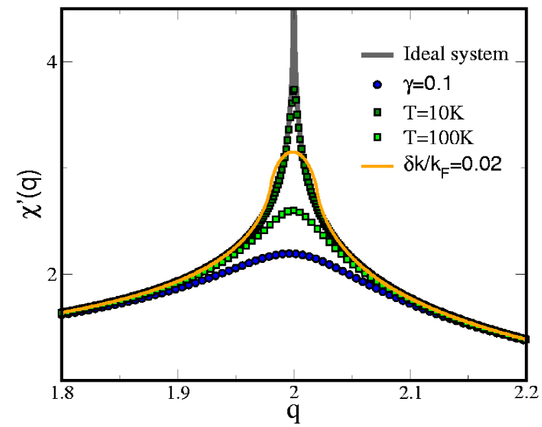
This expression is normalized to at (the overall scale is not important at the moment) and has a very weak, logarithmic divergency at To illustrate just how weak it is, we assume a relaxation rate corresponding to the Drude relaxation rate in optics, and recalculate . The new result reads:
| (10) |
The divergency has been reduced to merely an enhancement of over by a factor of For typical of the order of 0.1-0.2 eV this enhancement is by a factor of 2-2.5. One can also add that at any finite temperature, even without relaxation, For typical Fermi energies and T=10K (most observed ILTs occur at higher temperatures) the enhancement is again only a factor of the order of four.
Thus, carrier scattering and Fermi function broadening are suffucient to reduce the nesting-induced divergency to a minor structure in But an even more severe effect is caused by geometrical deviations of the Fermi surface from perfect nesting. A common procedure in the search for nesting vectors in a particular fermiology is to copy a quasi-2D Fermi surface cut onto transparent paper and slide it until some piece of the displaced Fermi surface visually coincides with another piece of the original plot. It is instructive to give a quantitative gauge of what constitutes a ”good nesting” vs. a ”bad nesting”. Assuming that the “nested” parts really nest only up to some in the reciprocal space, we observe, by averaging Eq.9, that
| (11) |
In the small limit, In other words, if 2D Fermi lines coincide within 5% of the Fermi vector, the corresponding enhancement of the susceptibility is about a factor of three. It is also important to remember that real materials are quasi-2D, not 2D. Any dispersion in the third direction of the order of brings us again to Eq.LABEL:2D. In a one-band case one can estimate the ratio as This shows that anything with a calculated transport anisotropy of less than one order of magnitude is 3D from a “nesting point of view”. Fig.1 illustrates the effect of various deviations from the perfect Peierls picture on the divergence of .
To further emphasize the non-role that FS nesting plays, let us investigate a system in which an ILT with has actually occurred, and as a result a gap equal to has opened, with the corresponding energy gain in the one-electron energy. The common wisdom is that energy is gained predominantly near the former Fermi energy, where the lowering of one-electron states is the largest. But, is this really so? In first order perturbation theory, the new one-electron spectrum is
| (12) | |||||
| (13) |
where is the energy shift of the state and is the energy difference between the two states connected by the nesting vector An inspection of this expression shows that integrating it over does not diverge at (that is, at the Fermi energy), but would diverge at large energies, , if the integration were not limited by the bandwidth. Substituting we get
| (14) |
The total energy gain, is:
| (15) |
The first term corresponds to integrating over the region and neglecting and the second corresponds to integrating over the region and neglecting terms smaller than In other words, the first (non-divergent) term comes from states near the Fermi level, where the gap opens up, and the second term (divergent at large ) comes from the rest of the states below the Fermi level and down to the bottom of the band. Since an actual instability is always a competition between an electronic (in this picture, one-electron) energy gain and an elastic energy loss, it is apparently more important to optimize the energy gain from all occupied states than to open a gap over the largest possible part of the Fermi surface.
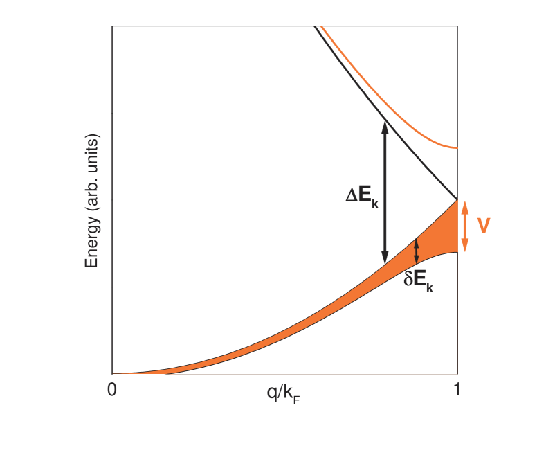
Since, as we have just found, all occupied states are important for a ILT, it is important to keep in mind the multiband character of real solids, and, correspondingly, the contribution of the interband transitions to To get a feeling for the interband effects, let us consider an insulating system which, instead of the free-electron band discussed above, has a fully occupied first neighbor tight-binding band, separated from a similar empty band by an energy , Let us assume for simplicity a constant interband dipole matrix element equal to unity. The susceptibility is given by
| (16) |
This susceptibility is enhanced at (at the edge of the BZ) compared to its minimum value (at by a factor of . This enhancement can be very large even for bands with a large relative shift. Using for example (giving a gap of 1/8 of the bandwidth), the enhancement is 2.2, quite comparable to what one might expect in a realistic nesting scenario. This demonstrates again that the Fermi surface topology is unlikely to be a factor in CDW formation. Note that the band structure that we have used is not special in any way, as opposed to the half-filled band exhibiting a Peierls instability.
II First principles calculations of real materials
In the following sections, we present three examples of real materials, commonly thought to be canonical examples of nesting-driven CDW systems: NbSe2, TaSe2, and CeTe3. Using first principles density functional theory calculations, we show that FS nesting is not the driving force behind the observed CDW in any of the three compounds. We additionally investigate a chain of Na ions and show that even for this artificially perfect 1D system, the strong FS nesting fails to produce any appreciable CDW when the ionic positions are fixed. This is perfectly in line with our contention that electron-phonon coupling is necessary to instigate the ILT and that even in the Peierls formulation, the resulting CDW is exponentially small.
For all investigated compounds, the first principles calculations were performed using the well-known Wien2K packageP. Blaha et al. (2002) with the local density approximation (LDA) to the exchange correlation potential J. P. Perdew and Y. Wang (1992) . For NbSe2 and TaSe2, it was found that spin-orbit coupling has a finite effect on the band structure and Fermi surface and therefore was taken into account. To get a good energy mesh, we calculated eigenvalues at nearly 15,000 points in the full BZ. For CeTe3, the partially filled -states pose a well-known problem for the mean-field LDA methodology by partially filling each of the states rather than completely filling some and emptying all others. We have addressed this shortcoming by using LDA+U in the fully localized limit scheme V. I. Anisimov et al. (1991). We applied a U of 4.5 eV and successfully reproduced the state observed by magnetization measurements Y. Iyeiri et al. (2003) for the Ce ion, simultaneously removing all bands from the Fermi energy. None of the quantities we calculate are expected to be sensitive to the precise value of U and we did not investigate the effects of changing it. We used a mesh of approximately 30,000 points in the full BZ to calculate the energy eigenvalues used for the susceptibilities. For all compounds, we used a temperature smearing of 2 mRy during numerical integration. For calculation of the chain of Na atoms we used the Vienna Ab-Initio Simulation (VASP) package with the projector augmented wave (PAW) basis set G. Kresse and J. Furthmuller (1996); P. E. Blochl (1994); G. Kresse and D. Joubert (1999). We used several different pseudopotentials with varying levels of hardness for the Na core, all giving identical results to within the accuracy of our calculations.
II.1 NbSe2 and TaSe2
Quasi-two-dimensional NbSe2 belongs to a family of layered dichalcogenides that undergoes a CDW transition sometimes thought to be related to FS nesting. A calculation of both the real and imaginary parts of the one-electron susceptibility M. D. Johannes et al. (2006) shows this to be unequivocally not the case. Although FS nesting does exist and does produce a peak in , it is located at = (1/3,1/3,0) and not at the observed = (1/3,0,0) (See Ref M. D. Johannes et al., 2006 for pictures). On the other hand, a weak peak at appears in . This peak is not strong enough alone to stimulate the observed CDW transition, but must be assisted by electron-phonon coupling at the same wave vector. To verify this, we performed two first principles calculations of NbSe2 in a supercell corresponding to the observed CDW vector. In one case, we clamp the ions to their high symmetry positions and in the other we allow them to shift. When allowed, the ions do indeed shift and an instability at the right wave vector, (1/3,0,0), is reproduced. In the case where the ions are forced to be stationary, both ionic and electronic systems remain stable in their high symmetry states. Even if we prompt the electronic system by artificially redistributing the charge along the known CDW direction, it relaxes back to its high symmetry state. Our calculations on this system provide a clear example of the lack of influence of Fermi surface nesting with respect to CDWs: a strong FS nesting that produces a sharp peak fails to gives rise to a CDW at the associated wave vector, while a peak wholly unrelated to FS nesting but at the correct vector appears in the real part of the susceptibility and, in conjunction with electron-lattice effects (but not without!) does produce a CDW.
We have also investigated an isostructural material, TaSe2, that has an observed CDW at approximately the same wave vector as NbSe2. The Fermi surface of the Ta compound is different from that of NbSe2, as was most recently observed by Rossnagel et al K. Rossnagel et al. (2005) who also point out that the measured surface differs from the calculated one K. Rossnagel et al. (2005); S. V. Borisenko et al. (2007); G. Wexler and A. M. Wolley (1976). This is somewhat surprising because calculated and observed Fermi surfaces are in quite good agreement for NbSe2. One reason for the discrepancy between NbSe2 and TaSe2 and between theory and experiment is spin-orbit coupling, which is strong for the heavy Ta ion. This coupling has not been included in most previously published TaSe2 band structures and Fermi surfaces G. Wexler and A. M. Wolley (1976); A. H. Reshak and S. Auluck (2005); R. L. Barnett et al. (2006), with the result that they differ less than they should from NbSe2 band structures. The spin-orbit interaction non-trivially changes the band dispersion near the Fermi energy, particularly along and leads to a different Fermi surface topology. Scalar relativistic effects are responsible for the lower Se band in TaSe2 (compared to NbSe2) which removes it from the Fermi surface entirely. Although we include both scalar relativistic effect and spin-orbit coupling in our calculations and find qualitative differences between the Nb and Ta di-selenides, we still find that the TaSe2 Fermi surface differs somewhat from the ARPES observed surface. However, nearly perfect agreement can be achieved by a small shift of the Fermi energy (about 0.04 eV). In Fig. 3, the Fermi surface both with and without the small shift in Fermi energy is shown.
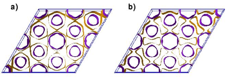
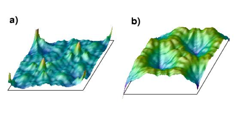
The susceptibilities presented here are calculated using the Fermi energy shift necessary to bring theoretical and experimental Fermi surfaces into agreement, but in fact this shift has no visible effect whatsoever on either the real or imaginary parts, despite its dramatic effect on the FS topology. In Fig.4, the real and imaginary parts of the susceptibilities for TaSe2 are presented. Looking at the susceptibilities in Fig.4, one can see some similarity between the peak structures in this compound and in NbSe2 M. D. Johannes et al. (2006), most particularly in the location of the nesting-driven peak in vs. the peak in . Again we find that the peaks are in different locations, indicating that nesting cannot give rise to a charge instability.
A recent study of these two materials K. Rossnagel et al. (2005) concluded that both materials have CDWs driven by strong electron-phonon coupling in the presence of weak nesting. Our calculations show that, indeed, electron-phonon coupling is behind the transition, but we can eliminate Fermi surface nesting from the phenomenon entirely. There is no nesting at all, not even weak, at the CDW wave vector. The electronic susceptibility structure, which is indeed favorable to a CDW at the right wave vector, is due to finite energy electronic transitions and not to a Fermi surface geometry.
II.2 CeTe3
CeTe3 is another layered material, (see Fig.5) also belonging to a family of compounds RTe3, R = rare earth, all of which exhibit CDWs E. DiMasi et al. (1995); A. Sacchetti et al. (2007); V. Brouet et al. (2004). The two-dimensionality is considerably stronger in this series than in the dichalcogenides discussed above, producing an easily visible Fermi surface nesting between strongly two-dimensional Fermi sheets. As in the former series, the strongest nesting peaks seen in produced by this nesting are far away from and do not carry over into . However, much weaker peaks associated with a different nesting do appear in at the observed CDW wave vector and are then strongly enhanced by contributions away from the Fermi energy to eventually produce peaks in . It is an interesting and instructive exercise to track down the origin of both kinds of nesting peaks to examine why the strongest ones are irrelevant and why the weaker peaks are present throughout the energy spectrum, finally resulting in a peak in . To begin, we describe how the structure of the CeTe3 very simply gives rise to its Fermi surface. CeTe3 is composed of two different types of layers: those containing staggered Ce and Te ions and those containing Te ions only (see Fig.5). The states near the Fermi energy have predominantly Te character and come from the pure Te layers. Assuming a nearest neighbor only tight binding model of Te and orbitals (See Fig.5b) in these layers with 5 as in Fig.5b, we produce the crosshatched pattern of slightly warped one-dimensional Fermi sheets shown in Fig.5c. This model and the values of the tight-binding parameters are very similar to those developed in Ref. H. Yao et al., 2006.
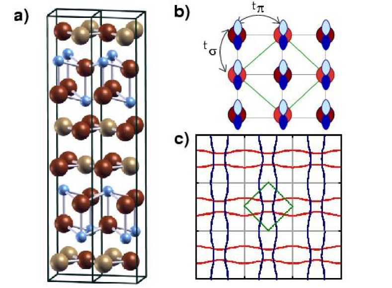
Nearest neighbor Te ions are inequivalent due to symmetry breaking imposed by the stacking of layers along the third direction. This results in a larger unit cell and a smaller, rotated BZ, shown superimposed in Fig.5c. The full, calculated FS is shown in Fig.6. A very good facsimile of it is achieved by folding the quasi-1D sheets of our TB model down into the new zone. Though small gaps appear during the folding down process, the long 1D ribbons are still clearly visible and both the nesting peak and the peak in can be traced back to these sheets.
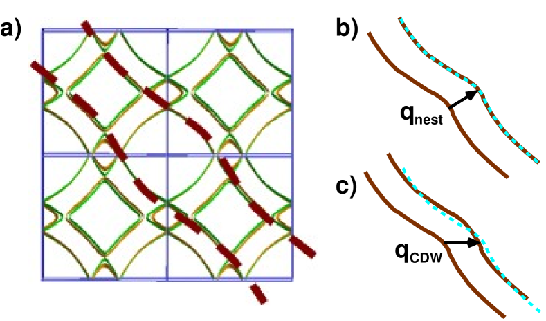
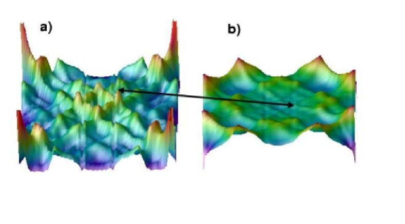
As can be seen by the cartoons in Fig.6, there is an excellent (ideally perfect in the nearest-neighbor TB model) FS nesting between two of the quasi-1D ribbons along the (110) direction of the BZ. This produces very sharp nesting-derived peaks in , away from the observed nesting vector. A moderate peak at = is visible, but by far the strongest peaks are located elsewhere in the Brillouin zone. Any CDW directly stemming from FS nesting would occur first at wave vectors corresponding to these alternate spots rather than at the observed . In the real part of the susceptibility, the strongest FS nesting peaks are suppressed dramatically, leaving only a peak at the correct wave vector (Fig.6). This is entirely due to an effect of the finite-energy transitions (note the non-zero value of terms in Eq. 1 even for widely spaced eigenvalues) that appear in the real part of susceptibility but not in the nesting function (imaginary part). The reason that the bulk of the peak height at = comes from contributions away from the Fermi energy can be understood by an examination of the band structure: the velocities of the electronic states connected by ( and ) are nearly equal and opposite at the Fermi energy (note that for the wave vector in Fig.6b, the opposite is true, and have the same sign). Therefore nearby states and are also of equal energy and are connected by . These are located above and below the Fermi energy respectively and do not contribute to the nesting function but do contribute to the real part of the susceptibility. This phenomenon has been pointed out earlier in Ref. M. -H. Whangbo et al., 1991 under the title of ’hidden nesting’. Obviously, if there are regions of the energy spectrum with equal and opposite velocities, they will contribute heavily to even if they are imperfectly nested at the Fermi energy itself. On the other hand, strong nesting between states exactly at the Fermi energy may die away quickly in other parts of the energy spectrum and contribute little to . This is the essence of why well nested Fermi surfaces fail to produce a peak in not only for CeTe3 but also for the dichalcogenides discussed in the previous section. The Fermi surface is simply too small a part of the energy range from which collects to have a decisive effect.
II.3 Na chain
To best approximate a perfect Peierls system, we calculated the ground state of a chain of Na ions separated by 38 in the two non-chain directions. The Na-Na distance was relaxed along the chain to its optimal value of 3.34 . As we saw previously with NbSe2, no CDW could be stabilized if the ions were clamped to their high symmetry positions, even though this system is ideal in every respect, i.e. the electronic-only CDW is unstable even when no mitigating factors such as higher dimensionality or imperfect nesting are present. Surprisingly, a relaxation of the ionic positions along the one-dimensional chain also failed to produce any deviation from the high symmetry, equally spaced arrangment, even when an initial dimerization was imposed. However, when the ions were allowed a larger dimensional freedom, the system distorted into a zigzag configuration as shown in Fig. 8. The ions in the zigzag arrangement are 3.43 apart and the angle formed by the distortion is 152 degrees. Although this distortion doubles the unit cell and lowers the total energy, it does not create the expected gap at EF. The coupling between matrix elements at the BZ boundary (k=) that would give rise to a gapped system does not occur because the distortion is two dimensional, while the wavefunctions are one-diemnsional. Thus, integration over the direction perpendicular to the chain in the dimension in which the distorion occurs drives the matrix element to zero. Precisely the same result can be obtained using a tight-binding formulation. Regardless of the number of neighbors included in the model, the states at the edge of the BZ remain degenerate, i.e. there is no gap. On the other hand, an enforced dimerization of the ions does produce a gap at EF, but is unstable. The true origin of the two-dimensional distortion is not yet entirely clear, but the Peierls mechanism can be ruled out. Thus, under perfect conditions, no electronic-only CDW forms, and no electron-ion interaction assisted CDW forms either. This indicates that the Peierls formulation is even weaker than we originally set out to prove. Not only do small deviations from the ideal system destroy the divergence that is purported to cause CDW formation, but in the ideal case itself, where no such deviations are present, the existence of ion cores is enough to effectively nullify the Peierls instability.

III Summary
To summarize, we have first explored the standard half-filled one-dimensional free electron system from the perspective of a Peierls distortion and have shown that the divergence in the real part of the susceptibility, caused by Fermi surface nesting, is exceedingly fragile. Effects such as temperature, imperfect nesting, or scattering, all of which are expected to be operative in a real material, reduce the divergence to a simple peak, often not more than a factor of two or three enhanced over the baseline susceptibility at q0. Thus, expectations of a CDW transition driven entirely by a Fermi surface nesting in any real material are unrealistic from the outset. Next, we have examined a system in which a gap at the Fermi surface has already been opened due a commensurate or incommensurate lattice transition, and found that the energy gain comes largely from the lowering of already filled states located away from the Fermi energy and not from removing states from the Fermi energy itself. This reinforces our contention that the Fermi surface topology plays at best a secondary role in CDW formation. Using first principles calculations, we take three examples of well-known CDW materials to illustrate our point and in each case we find that Fermi surface nesting either does not exist at the CDW wave vector, or is not the strongest nesting in the system. We further find that the CDW instability is not fundamentally electronic, but rather stems from strong electron-phonon interaction which, of course, is itself affected by the electronic structure.. Finally, we examine the canonical Peierls system, a one-dimensional chain of atoms, and find that the expected dimerization along the chain axis with any realistic amplitude is energetically unfavorable. The expected doubling of the unit cell occurs only if the one-dimensionality is relaxed to allow a zigzag, rather than dimerized, distortion. We conclude that no true distinction between CDWs and structural phase transitions, in particular incommensurate lattice transitions, can be made. Inspecting the Fermi surface itself for possible nesting features, without actually calculating the real part of electronic susceptibility has no predictive power for such structural transitions. Calculating the real part of the electronic susceptibility may be helpful in analyzing such instabilities, but only in relatively few cases can it be accepted as the only or even the main driving force for such transitions.
Acknowledgements.
We are especially grateful for the suggestions and advice of W.E. Pickett whose input has greatly improved this work. We also acknowledge several useful and enjoyable discussions with I.R. Fisher and his collaborators at Stanford, as well as helpful communications with S.V. Borisenko. Funding for research at NRL comes from the Office of Naval Research.References
- C. Battaglia et al. (2005) C. Battaglia, H. Cercellier, F. Clerc, L. Despont, M. G. Garnier, C. Koitzsch, P. Aebi, H. Berger, L. Forro, and C. Ambrosch-Draxl, Phys. Rev. B 72, 195114 (2005).
- E. Sandre et al. (2001) E. Sandre, P. Foury-Leylekian, S. Ravy, and J. P. Pouget, Phys. Rev. Lett. 86, 5100 (2001).
- J. Matsuno et al. (2001) J. Matsuno, A. Fujimori, L. F. Mattheiss, R. Endoh, and S. Nagata, Phys. Rev. B 64, 115116 (2001).
- M. -H. Whangbo et al. (1991) M. -H. Whangbo, E. Canadell, P. Foury, and J. P. Pouget, Science 252, 96 (1991), in this paper, a concept of ”hidden nesting” was introduced to account for the situation where no nesting in the FS topology is present, yet the real part of the susceptibility has a peak due to finite-energy transitions.
- P. Aebi et al. (2001) P. Aebi, Th. Pillo, H. Berger, and F. Levy, J. Electron Spectrosc. Relat. Phenom 117, 433 (2001).
- S-K. Chan and V. H. Heine (1973) S-K. Chan and V. H. Heine, J. Phys. F 3, 795 (1973).
- J. A. Wilson et al. (1977) J. A. Wilson, F. J. DiSalvo, and S. Mahajan, Adv. Phys. 50, 1171 (1977).
- W. E. Pickett and P. B. Allen (1977) W. E. Pickett and P. B. Allen, Phys. Rev. B 16, 3127 (1977).
- S. Chiba and Y. Ono (2003) S. Chiba and Y. Ono, J. Phys. Soc. Japan 72, 1995 (2003).
- S. Biermann et al. (2005) S. Biermann, A. Poteryaev, A. I. Lichtenstein, and A. Georges, Phys. Rev. Lett. 94, 026404 (2005), note that in this paper, the authors explain that ”the formation of dynamical V-V singlest pairs” is necessary to open a gap, i.e. a molecular-type transition is required. Despite a qualitative difference between this mechanism and the one discussed in the original Peierls paper, this is often called a ”Peierls transition”, as in the title of this paper.
- S. V. Borisenko et al. (2007) S. V. Borisenko, A. A. Kordyuk, A. N. Yaresko, V.B. Zabolotnyy, D. S. Inosov, R. Schuster, B. Buchner, R. Weber, L. Patthey, and H. Berger, cond-mat/0704.1554 (2007).
- A. Landa et al. (2006) A. Landa, J. Klepeis, P. Soderlind, I. Naumov, O. Velikokhatnyi, L. Vitos, and A. Ruban, J. Phys.: Condens. Matter 18, 5079 (2006).
- C Koitzsch et al. (2004) C Koitzsch, J. Hayoz, M. Bovet, F. Clerc, L. Despont, C. Ambrosch-Draxl, and P. Aebi, Phys. Rev. B 70, 165114 (2004).
- D. Kasinathan et al. (2006) D. Kasinathan, J. Kunes, A. Lazicki, H. Rosner, C. S. Yoo, R. T. Scalettar, and W. E. Pickett, Phys. Rev. Lett. 96, 047004 (2006).
- F. Clerc et al. (2006) F. Clerc, C. Battaglia, M. Bovet, L. Despont, C. Monney, H. Cercellier, M. G. Garnier, P. Aebi, H. Berger, and L. Forro, Phys. Rev. B 74, 155114 (2006).
- J. Kunes and R. Laskowski (2004) J. Kunes and R. Laskowski, Phys. Rev. B 70, 174415 (2004).
- O. Yu. Kolesnychenko et al. (2005) O. Yu. Kolesnychenko, G. M. M. Heijnen, A. K. Zhuravlev, R. de Kort, M. I. Katsnelson, A. I. Lichtenstein, and H. van Kempen, Phys. Rev. B 72, 085456 (2005).
- J. Ashkenazi et al. (1989) J. Ashkenazi, W. E. Pickett, H. Krakauer, C. S. Wang, B. M. Klein, and S. R. Chubb, Phys. Rev. Lett. 62, 2016 (1989).
- M. D. Johannes et al. (2006) M. D. Johannes, I. I. Mazin, and C. A. Howells, Phys. Rev. B 73, 205102 (2006).
- R. Yeats and H. Kroemer (1976) R. Yeats and H. Kroemer, Phys. Rev. B 14, 3335 (1976).
- P. Blaha et al. (2002) P. Blaha, K. Schwarz, G. K. H. Madsen, D. Kvasnicka, and J. Luitz, Wien2k (2002), iSBN 3-9501031-1-2.
- J. P. Perdew and Y. Wang (1992) J. P. Perdew and Y. Wang, Phys. Rev. B. 45, 13244 (1992).
- V. I. Anisimov et al. (1991) V. I. Anisimov, J. Zaanen, and O. K. Andersen, Phys. Rev. B 44, 943 (1991).
- Y. Iyeiri et al. (2003) Y. Iyeiri, T. Okumura, C. Michioka, and K. Suzuki, Phys. Rev. B 67, 144417 (2003).
- G. Kresse and D. Joubert (1999) G. Kresse and D. Joubert, Phys. Rev. B 59, 1758 (1999).
- G. Kresse and J. Furthmuller (1996) G. Kresse and J. Furthmuller, Phys. Rev. B 54, 11169 (1996).
- P. E. Blochl (1994) P. E. Blochl, Phys. Rev. B 50, 17953 (1994).
- K. Rossnagel et al. (2005) K. Rossnagel, E. Rotenberg, H. Koh, N. V. Smith, and L. Kipp, Phys. Rev. B 72, 121103(R) (2005).
- G. Wexler and A. M. Wolley (1976) G. Wexler and A. M. Wolley, J. Phys. C 9, 1185 (1976).
- A. H. Reshak and S. Auluck (2005) A. H. Reshak and S. Auluck, Physica B 358, 158 (2005).
- R. L. Barnett et al. (2006) R. L. Barnett, A. Polkovnikov, E. Demler, W.-G. Yin, and W. Ku, Phys. Rev. Lett 96, 026406 (2006).
- A. Sacchetti et al. (2007) A. Sacchetti, E. Arcangeletti, A. Perucchi, L. Baldassarre, P. Postorino, S. Lupi, N. Ru, I.R. Fisher, and L. Degiorgi, Phys. Rev. Lett. 98, 026401 (2007).
- E. DiMasi et al. (1995) E. DiMasi, M. C. Aronson, J. F. Mansfield, B. Foran, and S. Lee, Phys. Rev. B 52, 14516 (1995).
- V. Brouet et al. (2004) V. Brouet, W. L. Yang, X. J. Zhou, Z. hussain, N. Ru, K. Y. Shin, I. R. Fisher, and Z. X. Shen, 93, 126405 (2004).
- H. Yao et al. (2006) H. Yao, J. A. Robertson, E.-A. Kim, and S. A. Kivelson, Phys. Rev. B 74, 245126 (2006).