Graphite and graphene as perfect spin filters
Abstract
Based upon the observations (i) that their in-plane lattice constants match almost perfectly and (ii) that their electronic structures overlap in reciprocal space for one spin direction only, we predict perfect spin filtering for interfaces between graphite and (111) fcc or (0001) hcp Ni or Co. The spin filtering is quite insensitive to roughness and disorder. The formation of a chemical bond between graphite and the open -shell transition metals that might complicate or even prevent spin injection into a single graphene sheet can be simply prevented by dusting Ni or Co with one or a few monolayers of Cu while still preserving the ideal spin injection property.
pacs:
72.25.-b,73.43.Qt,75.47.-m,81.05.Uw,85.75.-dThe observation Baibich et al. (1988); Binasch et al. (1989) of giant magnetoresistance (GMR) in systems where the transmission through interfaces between normal and ferromagnetic metals (FM) is spin-dependent has driven a major effort to study spin filtering effects in other systems. An ideal spin filter would allow all carriers with one spin through but none with the other spin. Interfaces with half-metallic ferromagnets (HMFs) de Groot et al. (1983) should have this property but progress in exploiting it has been slow because of the difficulty of making stoichiometric HMFs with the theoretically predicted bulk properties and then making devices maintaining these properties at interfaces Dowben and Skomski (2004).
If the nonmagnetic metal (NM) is replaced by an insulator (I) or semiconductor (SC), spin filtering still occurs giving rise to tunneling magnetoresistance (TMR) in FMIFM magnetic tunnel junctions (MTJs) and spin-injection at FMSC interfaces. If the spin-polarization of the ferromagnet is not complete, then the conductivity mismatch between metals and semiconductors or insulators has been identified as a serious obstacle to efficient spin injection Schmidt et al. (2000). It can be overcome if there is a large spin-dependent interface resistance but this is very sensitive to the detailed atomic structure and chemical composition of the interface. Knowledge of the interface structure is a necessary preliminary to analyzing spin filtering theoretically and progress has been severely hampered by the difficulty of experimentally characterizing FMI and FMSC interfaces.
| Graphene | Co | Ni | Cu | |
|---|---|---|---|---|
| (Å) | 3.544111Ref.Ibach and Lüth, 1995 | 3.524111Ref.Ibach and Lüth, 1995 | 3.615111Ref.Ibach and Lüth, 1995 | |
| (Å) | 2.46 | 2.506 | 2.492 | 2.556 |
| (Å) | 2.45 | 2.42 | 2.42 | 2.49 |
| (Å) | 3.30 | 2.04 | 2.03 | 3.18 |
| (eV) | 0.10 | 0.37 | 0.32 | 0.07 |
| (eV) | 4.6 | 5.4 | 5.5 | 5.2 |
| (eV) | 4.6222Ref.Oshima and Nagashima, 1997 | 5.0333Ref.Michaelson, 1977 | 5.35333Ref.Michaelson, 1977 | 4.98333Ref.Michaelson, 1977 |
The situation improved with the confirmation of large values of TMR in tunnel barriers based upon crystalline MgO Yuasa et al. (2004); Parkin et al. (2004) which had been predicted by detailed electronic structure calculations Butler et al. (2001); Mathon and Umerski (2001). While the record values of TMR - in excess of 500% at low temperatures Yuasa et al. (2006) - are undoubtedly correlated with the crystallinity of MgO, the nature of this relationship is not trivial Tsymbal et al. (2007). The sensitivity of TMR (and spin injection) to details of the interface structure Zwierzycki et al. (2003); Xu et al. (2006) make it difficult to close the quantitative gap between theory and experiment. In view of the reactivity of the open-shell transition metal (TM) ferromagnets Fe, Co and Ni with typical semiconductors and insulators, preparing interfaces where disorder does not dominate the spin filtering properties remains a challenge. With this in mind, we wish to draw attention to a quite different material system which should be intrinsically ordered, for which an unambiguous theoretical prediction of perfect spin filtering can be made in the absence of disorder, and which is much less sensitive to interface roughness and alloy disorder than TMR or spin injection.
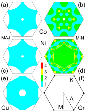
We begin by observing that the in-plane lattice constants of graphene and graphite match the surface lattice constants of (111) Co, Ni and Cu almost perfectly. From Table 1, it can be seen that Ni is particularly suitable with a lattice mismatch of only 1.3%. The second point to note is that the only electronic states at or close to the Fermi energy in graphene or graphite are to be found near to the high symmetry K point in reciprocal space where Co and Ni have states with minority spin character only. The absence of majority spin states in a large region about the K point is made clear in the (111) Fermi surface (FS) projections shown in Fig. 1. The (0001) FS projections for hcp Co are qualitatively the same. It follows that in the absence of symmetry-lowering (resulting from disorder, interface reconstruction etc.) perfect spin filtering should occur for graphite on top of a flat Ni or Co (111) surface.

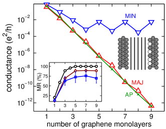
The effectiveness of the spin filtering is tested for a current-perpendicular-to-the-plane (CPP) structure with graphene layers sandwiched between semi-infinite Ni electrodes. The spin dependent transmission through this NiGrNi junction is calculated using a first-principles tight-binding muffin tin orbital (TB-MTO) wave-function matching scheme Xia et al. (2001, 2006) for parallel (P) and antiparallel (AP) orientations of the Ni magnetizations. The atomic sphere (AS) potentials are calculated self-consistently within density functional theory for atomic structures determined by total energy minimization (see below). The conductances and are shown in Fig. 2 for the minority and majority spin channels, min, maj. and are strongly attenuated while, apart from an even-odd oscillation, is independent of . The magnetoresistance MR rapidly approaches 100%; see inset. We use the pessimistic definition of MR because vanishes for large ; usually the optimistic version is quoted Yuasa et al. (2004); Parkin et al. (2004); Butler et al. (2001); Mathon and Umerski (2001); Yuasa et al. (2006). Similar results are obtained for NiGrCo and CoGrCo junctions.

We envisage a procedure in which thin graphite layers are prepared by micromechanical cleavage of bulk graphite onto a SiO2 covered Si wafer Geim and Novoselov (2007) into which TM (Ni or Co) electrodes have been embedded and layers of graphene are peeled away until the desired value of is reached. Assuming it will be possible to realize one essentially perfect interface in a CPP geometry, we studied the effect of roughness and disorder at the other interface on MR (inset Fig. 2). Replacing the top Ni layer with a Ni50Cu50 random alloy only reduces the MR to 90% (900% in the optimistic definition). Extreme roughness, whereby half of the Ni interface layer is removed at random, only reduces the MR to 70%. The momentum transfer induced by the scattering is apparently insufficient to bridge the large gap about the K point in the majority spin FS projections. Alternatively, it may be possible to prepare two separate, near-perfect TMGr interfaces and join them using a method analogous to vacuum bonding Monsma et al. (1998).
Graphite has a large -axis resistivity Matsubara et al. (1990). If one of the TMGr interfaces is ideal and the graphite layer is sufficiently thick, then it should be possible to achieve 100% spin accumulation in a high resistivity material making it suitable for injecting spins into semiconductors Schmidt et al. (2000). Because carbon is so light, spin-flip scattering arising from spin-orbit interaction should be negligible.
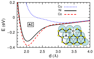
The results shown in Fig. 2 were calculated for the lowest energy “AC” configuration of graphene on Ni corresponding to one carbon atom above a Ni atom (the surface “A” sites) while the other is above a third layer Ni “C” site. A and C refer to the conventional ABC stacking of the layers in an fcc crystal (AB for an hcp structure). The CPP spin filtering should not depend on the details of how graphite bonds to the metal surface as long as the translational symmetry parallel to the interfaces is preserved. This is confirmed by explicit calculation for the “AB” and “BC” bonding configurations for varying graphene-metal surface separation .

The nature of the bonding may well play an important role in realizing such an interface experimentally. In Fig. 3 we show the total energy of a graphene sheet on TM = Co, Ni and Cu (111) surfaces as a function of where the zero of energy has been chosen so that for an uncharged graphene sheet. The density functional theory (DFT) calculations were carried out using the projector augmented wave (PAW) method Blöchl (1994); Kresse and Joubert (1999), a plane wave basis set and the LDA, as implemented in the VASP program Kresse and Hafner (1993); Kresse and Furthmuller (1996). Supercells containing a slab of at least six layers of metal atoms with a graphene sheet adsorbed on one side of the slab and a vacuum region of Å were used. The Brillouin zone of the surface unit cell was sampled using a -point grid. The plane wave kinetic energy cutoff was 400 eV. To avoid interactions between periodic images of the slab a dipole correction was applied Neugebauer and Scheffler (1992). The atoms in the metal layers were fixed at their bulk positions. The experimental lattice constant of graphene Å is used as the lattice parameter for Co, Ni and Cu. To plot the band structures (Fig. 4), a 13 layer slab with graphene absorbed on both sides was used.
The most prominent feature of Fig. 3 is the prediction of a weak minimum in the binding energy curve for Cu of about 0.07 eV at an equilibrium separation Å and deeper minima of 0.37 and 0.32 eV respectively for Co and Ni, at a smaller equilibrium separation of Å. In agreement with a recent first-principles calculation Bertoni et al. (2005) and experiment Gamo et al. (1997); Oshima and Nagashima (1997) for graphene on Ni, we find that the lowest energy corresponds to an AC configuration. The finer details of the total energy surfaces depend on the choice of exchange-correlation potential, relaxation of the metal substrate, choice of in-plane lattice constant etc. and will be presented elsewhere. We restrict ourselves here to properties which do not depend on these details.

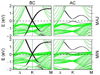
The electronic structure of a single graphene layer does depend on . For the less strongly bound BC configuration of Gr on Ni, the equilibrium separation is Å and the characteristic band structure of an isolated graphene sheet is clearly recognizable; see Fig. 4. For the lowest energy AC configuration, the interaction between the graphene sheet and Ni surface is much stronger, a gap is opened in the graphene derived bands and there are no graphene states at the K point in reciprocal space at the Fermi energy for the minority spin channel. This may prevent efficient spin injection into graphene in lateral, current-in-plane (CIP) devices Hill et al. (2006). However, there is a simple remedy. If a monolayer (or several layers) of Cu is deposited on Ni, graphene will form only a weak bond with Cu and the Fermi energy graphene states at the K point will only be weakly perturbed. Cu will attenuate the conductance of both spin channels because Cu has no states at the K point but will not change the spin injection properties as long as it is sufficiently ordered as to preserve the translational symmetry; a completely mixed CuNi top layer reduces the MR in a NiGrCu50NiNi junction only slightly (Fig. 2). Cu will also oxidize less readily than the more reactive Ni or Co. Spin-flip scattering in a thin layer of Cu can be neglected. The weaker bonding of graphene to Cu may also have practical advantages in sample preparation.
Finally, we remark that graphene may exhibit curious bonding properties to a (111) surface of a Cu1-xNix or Cu1-xCox alloy; as a function of increasing concentration , the weak minimum at Å will evolve into a deeper minimum at Å with the possibility of a double minimum occuring for some range of concentration ; a propensity to form a second minimum is already evident in the binding energy curve for Cu. Calculations are underway to examine this possibility.
Planar interfaces between graphene and close-packed Co, Ni, or Cu represent a very flexible system for studying the influence of atomic and electronic structure on electrical contact with graphene related systems such as carbon nanotubes Schönenberger (2006) where the nanotube geometry is very difficult to model using materials specific calculations Nemec et al. (2006). The binding energy curves in Fig. 3 and electronic structures in Fig. 4 show that the closer proximity resulting from stronger bonding does not necessarily lead to better electrical contact if bonding removes the carbon-related conducting states from the Fermi energy.
Motivated by the recent progress in preparing and manipulating discrete, essentially atomically perfect graphene layers, we have used parameter-free, materials specific electronic structure calculations to explore the bonding and spin transport properties of a novel TMGrn system. We predict perfect spin filtering for ideal TMGrTM junctions with TM = Co or Ni.
Acknowledgments: This work is supported by “NanoNed”, a nanotechnology programme of the Dutch Ministry of Economic Affairs. It is part of the research programs of “Chemische Wetenschappen” (CW) and “Stichting voor Fundamenteel Onderzoek der Materie” (FOM) and the use of supercomputer facilities was sponsored by the “Stichting Nationale Computer Faciliteiten” (NCF), all financially supported by the “Nederlandse Organisatie voor Wetenschappelijk Onderzoek” (NWO). MZ wishes to acknowledge support from EU grant CARDEQ under contract IST-021285-2.
References
- Baibich et al. (1988) M. N. Baibich, J. M. Broto, A. Fert, F. Nguyen Van Dau, F. Petroff, P. Etienne, G. Creuzet, A. Friederich, and J. Chazelas, Phys. Rev. Lett. 61, 2472 (1988).
- Binasch et al. (1989) G. Binasch, P. Grünberg, F. Saurenbach, and W. Zinn, Phys. Rev. B 39, 4828 (1989).
- de Groot et al. (1983) R. A. de Groot, F. M. Mueller, P. G. van Engen, and K. H. J. Buschow, Phys. Rev. Lett. 50, 2024 (1983).
- Dowben and Skomski (2004) P. A. Dowben and R. Skomski, J. Appl. Phys. 95, 7453 (2004).
- Schmidt et al. (2000) G. Schmidt, D. Ferrand, L. W. Molenkamp, A. T. Filip, and B. J. van Wees, Phys. Rev. B 62, R4790 (2000).
- Yuasa et al. (2004) S. Yuasa, T. Nagahama, A. Fukushima, Y. Suzuki, and K. Ando, Nature Materials 3, 868 (2004).
- Parkin et al. (2004) S. S. P. Parkin, C. Kaiser, A. Panchula, P. M. Rice, B. Hughes, M. Samant, and S. H. Yang, Nature Materials 3, 862 (2004).
- Butler et al. (2001) W. H. Butler, X. G. Zhang, T. C. Schulthess, and J. M. MacLaren, Phys. Rev. B 63, 054416 (2001).
- Mathon and Umerski (2001) J. Mathon and A. Umerski, Phys. Rev. B 63, 220403(R) (2001).
- Yuasa et al. (2006) S. Yuasa, A. Fukushima, H. Kubota, Y. Suzuki, and K. Ando, Appl. Phys. Lett. 89, 042505 (2006).
- Tsymbal et al. (2007) E. Y. Tsymbal, K. D. Belashchenko, J. P. Velev, S. S. Jaswal, M. van Schilfgaarde, I. I. Oleynik, and D. A. Stewart, Progress in Materials Science 52, 401 (2007).
- Zwierzycki et al. (2003) M. Zwierzycki, K. Xia, P. J. Kelly, G. E. W. Bauer, and I. Turek, Phys. Rev. B 67, 092401 (2003).
- Xu et al. (2006) P. X. Xu, V. M. Karpan, K. Xia, M. Zwierzycki, I. Marushchenko, and P. J. Kelly, Phys. Rev. B 73, 180402(R) (2006).
- Ibach and Lüth (1995) H. Ibach and H. Lüth, Solid-State Physics (Springer-Verlag, Berlin, Heidelberg, 1995), 2nd ed.
- Oshima and Nagashima (1997) C. Oshima and A. Nagashima, J. Phys.: Condens. Matter. 9, 1 (1997).
- Michaelson (1977) H. B. Michaelson, J. Appl. Phys. 48, 4729 (1977).
- Xia et al. (2001) K. Xia, P. J. Kelly, G. E. W. Bauer, I. Turek, J. Kudrnovský, and V. Drchal, Phys. Rev. B 63, 064407 (2001).
- Xia et al. (2006) K. Xia, M. Zwierzycki, M. Talanana, P. J. Kelly, and G. E. W. Bauer, Phys. Rev. B 73, 064420 (2006).
- Geim and Novoselov (2007) A. K. Geim and K. S. Novoselov, Nature Materials 6, 183 (2007).
- Monsma et al. (1998) D. J. Monsma, R. Vlutters, and J. C. Lodder, Science 281, 407 (1998).
- Matsubara et al. (1990) K. Matsubara, K. Sugihara, and T. Tsuzuku, Phys. Rev. B 41, 969 (1990).
- Blöchl (1994) P. E. Blöchl, Phys. Rev. B 50, 17953 (1994).
- Kresse and Joubert (1999) G. Kresse and D. Joubert, Phys. Rev. B 59, 1758 (1999).
- Kresse and Hafner (1993) G. Kresse and J. Hafner, Phys. Rev. B 47, 558 (1993).
- Kresse and Furthmuller (1996) G. Kresse and J. Furthmuller, Phys. Rev. B 54, 11169 (1996).
- Neugebauer and Scheffler (1992) J. Neugebauer and M. Scheffler, Phys. Rev. B 46, 16067 (1992).
- Bertoni et al. (2005) G. Bertoni, L. Calmels, A. Altibelli, and V. Serin, Phys. Rev. B 71, 075402 (2005).
- Gamo et al. (1997) Y. Gamo, A. Nagashima, M. Wakabayashi, M. Terai, and C. Oshima, Surface Science 374, 61 (1997).
- Hill et al. (2006) E. W. Hill, A. K. Geim, K. Novoselov, F. Schedin, and P. Blake, IEEE Trans. Mag. 42, 2694 (2006).
- Schönenberger (2006) C. Schönenberger, Semiconductor Science and Technology 21, S1 (2006).
- Nemec et al. (2006) N. Nemec, D. Tomanek, and G. Cuniberti, Phys. Rev. Lett. 96, 076802 (2006).