Real space information from Fluctuation electron microscopy: Applications to amorphous silicon
Abstract
Ideal models of complex materials must satisfy all available information about the system. Generally, this information consists of experimental data, information implicit to sophisticated interatomic interactions and potentially other a priori information. By jointly imposing first-principles or tight-binding information in conjunction with experimental data, we have developed a method: Experimentally Constrained Molecular Relaxation (ECMR) that uses all of the information available. We apply the method to model medium range order in amorphous silicon using Fluctuation Electron microscopy (FEM) data as experimental information. The paracrystalline model of medium range order is examined, and a new model based on voids in amorphous silicon is proposed. Our work suggests that films of amorphous silicon showing medium range order (in FEM experiments) can be accurately represented by a continuous random network model with inhomogeneities consisting of ordered grains and voids dispersed in the network.
1 Introduction
The structural modeling of amorphous materials poses a particular challenge to condensed matter science. The initial hurdle to overcome is devising a computer model that accurately represents a small fragment of the material. Experimental data is inevitably the result of a system average involving macroscopic number of atoms in a continuously variable range of conformations. The result is that such data tend to be smooth with very limited information content. While the information provided by experiments is evidently of critical importance to understanding these materials, such information is incomplete (e.g., the information in the data is incapable of uniquely specifying the structure). The impressive advances in protein crystallography help to illustrate the challenge: in any crystalline system, diffraction measurements yield a palisade of functions. From the information entropy [1] it is easy to show that there is vastly more information in the sharply defined function for the crystal than the smooth function characteristic of a glass or amorphous material. The structure factor for the crystal is nearly sufficient to uniquely invert the data to obtain the structure, a stark contrast with the situation for amorphous materials. This argument also emphasizes the need to use all available experiments in modeling. Despite our lamentations about the limitations of information-based modeling, it is clearly wise to build models consistent with experimental information: our concern is that this information is highly incomplete by itself.
The limitations of information from experimental data beg for a molecular dynamics (MD) or Monte Carlo modeling approach using accurate interatomic interactions. If properly implemented, such a scheme will enforce the proper local ordering, chemistry etc. However, these approaches suffer from their own shortcomings: despite superficial similarities to the physical process of making a glass (quenching from the melt), such simulations are carried out with unphysically rapid quenches, models that are tiny (especially if accurate interactions are used), and of course the interactions themselves are never perfect. Despite these cautions, such simulations have met with many successes in a range of materials.
An ideal modeling approach should merge the information-based method and the computer simulation scheme. There is no unique way to accomplish this, and the “bottom line” is that whatever scheme is adopted, it must produce models that agree with all known information. We are aware of three efforts in this direction: our Experimentally Constrained Molecular Relaxation” (ECMR) method [2], a Bayesian method for biomolecules [3] and a related scheme used on amorphous carbon [4]. These methods vary in many details, but are similar in spirit and all have met with success in the problems approached.
Hydrogenated a-Si (a-Si:H) is one of the most important electronic materials [5]. While there is slight variability in pair-correlation functions measured for different samples, Fluctuation Electron Microscopy (FEM) experiments probing triplet or higher atomic correlations show dramatic variation from sample to sample. Even in this most venerable amorphous electronic material there is a lack of understanding about the difference in network topology on the medium range length scale between samples with different FEM data. In this paper we further develop our ECMR method to form models of a-Si including medium range order implied by Fluctuation Electron Microscopy (FEM) measurements.
2 The Inverse problems in materials modeling
The inverse approach takes a very different route to model materials. The focus here is on available experimental information pertaining to the materials under study. The challenge is to construct a model that is consistent with a given set of experimental data, and additionally an approximate total energy functional. In the context of materials modeling, the primary interest is on structure determination and the resulting electronic properties, but the formalism is also useful to construct empirical potentials [6, 7]. Although there exists no general proof that a many-body potential can be constructed uniquely within this approach, Henderson has shown a connection between pair potentials and radial distributions that states for a system under given temperature and pressure two pair potentials that produce same radial distribution functions can differ only by an additive constant [8]. Lyubartsev and Laaksonen have followed this idea to construct interaction potentials from radial distribution functions via reverse Monte Carlo simulation and apply it to aqueous sodium chloride (NaCl) solution [6]. Soper has developed empirical potential structure refinement (EPSR) where total diffraction data can be inverted into a set of partial structure factors by extending an earlier method of Edwards and Enderby [9] and reverse Monte Carlo method [7]. Zunger has recently applied the inverse band structure approach to find atomic configurations for a given set of electronic and optical properties in alloys [10].
The reverse Monte Carlo (RMC) method developed by McGreevy and coworkers describes how to construct a physical structure (i.e. a 3-dimensional model) of a material using the information included in the structure factors [11, 12, 13, 14]. Instead of using any conventional energy functional, a generalised penalty function is constructed involving experimental structural data and some suitable constraints, which is then minimized by using the Metropolis Monte Carlo algorithm [15]. The set of configurations obtained in this method can be used for further analysis of structural, electronic and vibrational properties. The method does not generate interaction potentials and in absence of sufficient information, configurations obtained from RMC may not be physically meaningful. One usually addresses this problem by adding further information, but often this proves to be difficult to optimize via simple Monte Carlo scheme.
ECMR has been designed to overcome some of the problems above [2]. Mathematically, ECMR offers an approximate solution to the constrained optimization problem: Find a set of coordinates that is a minimum of an accurate energy functional subject to the constraint that the coordinates reproduce one or more experimental data sets. In practice it may be useful to impose other constraints too, for example on atomic coordination or chemical order. In the following, we apply ECMR to model medium range order using FEM data as experimental information and an empirical total energy functional.
3 Modeling medium range order as an inverse problem
Medium range order (MRO) is defined as structural ordering that exists between the short range (typically 3-5 Å) and the long range ( Å) length scale [16]. Quantifying order at this length scale is somewhat ambiguous and requires information beyond radial (pair) distribution functions. Until recently, there has been a very few direct experimental evidence to detect MRO. In ionic and covalent glasses, MRO manifests itself in the first sharp diffraction peak (FSDP) of the total factor structure factor [17]. This feature corresponds to real space ordering in materials at the intermediate length scale. The well known Staebler-Wronski effect is an example where creation of metastable dangling bonds in hydrogenated amorphous silicon upon exposure to visible light [18] has been observed to occur in the material with diminishing medium range order [19]. Fluctuation electron microscopy clearly reveals that structure of thin films of amorphous silicon are much more complex than a continuous random network model [20].
Higher order correlation functions are the most suitable candidates for studying the signature of MRO in amorphous networks. However, obtaining experimental structural information beyond the 2-body correlation function is non-trivial and there exists no simple and direct scheme of systematic analysis of the full 3- and 4-body correlation functions. Treacy and Gibson have addressed the problem experimentally by developing a low resolution electron microscopy technique known as fluctuation electron microscopy (FEM) [21]. FEM can detect MRO because it is sensitive to 3- and 4-body correlation functions. It was shown that the fluctuation in the diffracted intensities can be measured by the normalized variance of the intensities, and is directly related to 3- and 4-body correlation functions containing the information at the medium range length scale [20].
We apply our ECMR technique starting with two very different models of a-Si: the first is a paracrystalline model of amorphous Si proposed by Khare [22] and the second includes voids in continuous random networks. In our work, we start from each of these models and apply our ECMR method to obtain final configurations displaying FEM signal, which we call Model-A and Model-B respectively. In both the cases, one observes the presence of strong FEM signal, and the model is also consistent with other physical observables such as structure factors, electronic and vibrational density of states.
4 Paracrystalline models of medium range order
Before we proceed to model generation, we briefly mention the key equations of Fluctuation Electron Microscopy (FEM) that have been used here in conjunction with ECMR method to generate amorphous network containing medium range order. For a detailed description of FEM and ECMR, we refer to Refs [20, 21, 23] and Ref [2] respectively. In FEM, we estimate MRO by measuring the normalized variance of the dark-field image intensity instead of intensity itself. The normalized variance is defined as:
| (1) |
The variable is the magnitude of the scattering vector and defines the characteristic length scale of MRO. In a variable coherence microscopy, one fixes the value of and varies in order to determine the degree of MRO present in the length scale of inverse . Following Treacy and Gibson [19, 21], we are interested in the fluctuation in the intensity for varying at a fixed spatial resolution. The intensity due to scattering from a volume centered at r of size proportional to is given by [20],
| (2) |
where is the radial distribution function, is the coherence function describing incoming illumination, and is the microscope response function. The intensity in the above expression involves only and therefore does not carry information about MRO. It is the second moment of the intensity that includes 3- and 4-body correlation functions, which provide information at the medium range length scale. A mathematical expression of and its derivation is given by Voyles [20].
Computer simulations have recently indicated [20] that amorphous silicon or germanium films may contain some nano-sized crystalline grains embedded in a CRN matrix [24]. This model of amorphous silicon is called paracrystalline, and simulation of FEM data using these models have been observed to interpret experimental results [22, 24]. It is proposed that the size and shape of the grains are related to the height and position of the peaks in the FEM signal, and an appropriate concentration (typically 20% – 30% by number) of such crystalline grains in amorphous matrix can reproduce correct structural, vibration and electronic properties [25]. However, the model is not unique. Since we know from Reverse Monte Carlo simulation that it is possible to generate configurations of amorphous silicon having almost identical structure factor observed in experiment but with drastically different local bonding, it is necessary to explore the possibility of constructing models that do not explicitly contain nano-sized grains in the networks to start with. We have studied the problem along this direction via reverse Monte Carlo and modified Wooten-Winer-Weaire (WWW) [26] method and observed that direct inclusion of FEM signal in CRN introduces strain in the network [27]. The resulting network shows a strong FEM signal and maintains other properties of a-Si, but does not produce any visible ordering (such as distorted crystals that is expected from paracrystalline models) except occasional occurrences of few Schläfli clusters [28, 29]. It is instructive to study the stability of paracrystalline models via ECMR. To this end, we first generate a starting configuration containing grain(s) of diamond crystal by creating voids of nanometer size in a CRN, and then construct a generalized cost function involving FEM signal, a suitably chosen energy functional (modified Stillinger Weber potential [30]) and the structure factor as follows:
| (3) |
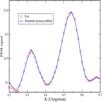
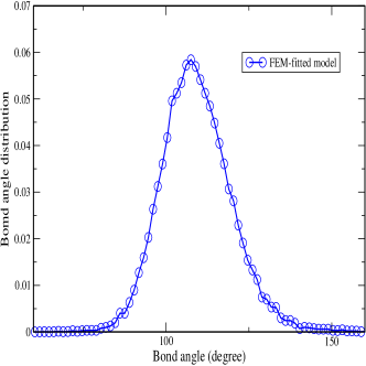
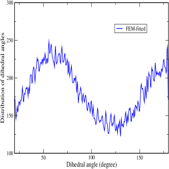
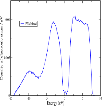
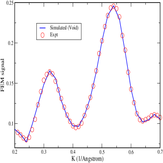
Here is the modified Stillinger-Weber potential, and stand for FEM data and structure factor respectively, and and are appropriate weight factors (for each data set) which may change during the course of simulation. Our starting configuration is a 4056-atom continuous random network that contains a 216-atom grain of diamond crystal. This starting configuration shows the presence of a weak FEM signal by construction. We minimize the cost function in equation (3) via Metropolis Monte Carlo algorithm by moving the crystal and interface atoms [31]. During the Monte Carlo minimization, the topological constraint of the crystaline grain is relaxed so that the atoms in the grain are free to evolve away from (diamond) crystalline geometry, and yet maintain other constraints (such as the FEM signal, structure factor etc.). The inclusion of the latter is important because of the difference in structure factors of crystalline and amorphous environment of Si. The use of modified Stillinger-Weber potential controls the network strain, and maintains the total energy of the system during Monte Carlo simulation as minimum as possible. In figure 1, we have plotted the simulated FEM signal obtained from the final configuration along with the experimental data. A structural analysis of this final configuration shows that the crystal and interface atoms have moved significantly to form a distorted ordered structure away from the perfect crystal. A Schläfli cluster analysis [28, 29] has shown the presence of cluster which originates from diamond crystal structure. The bond and dihedral angle distributions have been plotted in figures 3 and 4 respectively. No significant differences have been observed in the bond angle and dihedral distributions compared to its CRN counterpart. The electronic density of states (EDOS) for the final FEM-fitted model (Model-A) is plotted in figure 5 using a tight-binding model Hamiltonian. The density of electronic states show a gap with some states in the gap. This is due to the presence of few 3-fold and 5-fold coordination defects in the model.
5 Continuous random network with voids
A very different approach to understand the FEM signal and hence MRO in amorphous silicon is to study the presence of voids in the network structure. Voids are a universal feature in amorphous silicon, and the characteristic of voids depends largely on the growth condition of the materials. The presence of voids is considered to be one of reasons of low density of amorphous silicon compared to its crystalline counterpart [32]. Small angle scattering of neutrons, electrons, and X-rays have been widely used to detect the characteristic presence of voids in both amorphous and hydrogenated amorphous silicons [33]. Theoretical modeling of voids in amorphous silicon by Biswas et al. have indicated the presence of rapidly increasing structure factor for wave vectors below 1 Å-1, which is supported by experiments [34]. In this work, we have developed models with voids in large continuous random network and have studied the variation of FEM signal with different number of voids and its size.
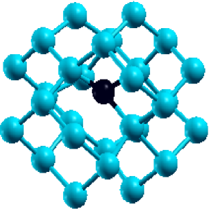
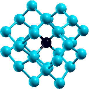
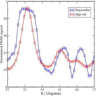
In order to test the viability of the model, we first start with a 1000-atom paracrystalline model and remove the grain of crystal. The resulting model continues to show the presence of FEM signal but the strength of the signal decreases as the wave vector increases. In figure 6, we have plotted the FEM signal for a paracrystalline model with and without the crystalline grain. It is clear from the figure that the first two peaks have not changed their positions and heights significantly. The formation of voids creates some coordination defects and introduces strain in the network, which can be minimized by structural relaxation of the network. Using the first-principles density functional code Siesta [35], we have relaxed the network to minimize the strain and to reduce the number of defects. While the surface of the voids reconstructs, the voids continue to exist in the relaxed model with a strong presence of the FEM signal. This observation suggests that presence of voids in amorphous network can also produce FEM signal as in paracrystalline model. Together with the presence of increasing structure factor at low wave vectors and FEM data, it appears that voids in amorphous silicon networks introduce some correlation that can affect the higher order correlation functions. Furthermore, introduction of voids does not change the other characteristic material properties significantly (such as vibration and electronic density of states). In figure 7 we have plotted the results obtained from a model containing a single void of radius 12 Å. Using our ECMR method, we have minimized the generalised penalty function (equation (3)) by moving the interface atoms. The void persists, but the surface of the void reconstructs to match with the normalized variance of intensity obtained from FEM experiments.
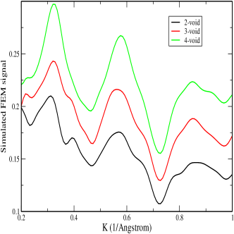
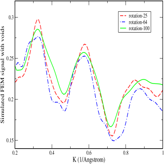
In figure 8, we have plotted the simulated FEM signal for different number of voids. The signal is observed to be maximum for four voids while minimum for two voids as shown in the figure. It is important to note that similar trends have been observed in case of paracrystalline model, where signal strength is observed to be dependent on the number of crystalline grains present in the sample. We have also studied the role of rotation of the sample for a model with given number of voids. The result is shown in the figure 9. For the model with four voids of linear size between 6 Å to 10Å, we find that the signal is more or less independent of 25 to 100 orientations of the model.
6 Conclusion
We have used Fluctuation Electron Microscopy data to incorporate medium range order in amorphous silicon starting with continuous random networks. We have discussed two models that are capable of producing the characteristic FEM signal observed in experiments maintaining structural, electronic and vibrational properties of amorphous silicon. The first model (Model-A) is consists of a CRN with nano-sized ordered grains in the network, while the second model (Model-B) is based on presence of voids in the network. Our study clearly indicates that the FEM signal is sensitive to the presence of small ordered grains and voids in the network. The FEM signal is found to be determined by fluctuations or inhomogeneities due to voids or phase-separated regions of nano-meter size dispersed in approximately homogeneous medium described by continuous random network. We have shown that either crystalline inclusions or voids are possible explanations for the measured FEM data.
References
- [1] Jaynes E T, Probability theory: the logic of science (Cambridge University Press, Cambridge, 2003).
- [2] Biswas P, Tafen D N, and Drabold D A, Phys. Rev.B 71 54204 (2005)
- [3] Habeck M, Rieping W, and Nilges M, Proc. Nat. Acad. USA 103 1756 (2006).
- [4] Opletal G, Peterson T C, McCulloch D G, Snook I K, and Yarovsky I, J. Phys. Cond. Matt. 17 2605 (2005).
- [5] Street R A, Hydrogenated Amorphous Silicon, Cambridge University Press, Cambridge 1991
- [6] Lyubartsev A P, and Laaksonen Astto, Phys. Rev.E 52, 3730 (1995)
- [7] Soper A K, Phys. Rev.B 72 104204 (2005)
- [8] Henderson R L, Phys. Lett. 49A, 197 (1974)
- [9] Edwards F G, Enderby J E, Howe R A, and Paige D I, J. Phys. C 8, 3483 (1975)
- [10] Dudiy S V, and Zunger Alex, Phys. Rev. Lett.97, 46401 (2006)
- [11] McGreevy R L, J. Phys.: Condens. Matter 13, R877 (2001).
- [12] Gereben O, and Pusztai L, Phys. Rev. B 50, 14 136 (1994).
- [13] Walters J K, and Newport R J, Phys. Rev. B 53, 2405 (1996).
- [14] Biswas P, Atta-Fynn R, and Drabold D A, Phys. Rev. B 69, 195207 (2004).
- [15] Metropolis N, Rosenbluth A W, Teller A H, and Teller E, J. Chem. Phys. 21, 1087 (1953)
- [16] Elliott S R, Physics of Amorphous Materials (Longman Group Limited Publication, United Kingdom, 2nd Revised Edition, 1990)
- [17] Elliott S R, Adv. Phys. 38, 1 (1989)
- [18] Staebler D, and Wronski C R, Appl. Phys. Lett 31, 292 (1977)
- [19] Gibson J M, Treacy M M J, Voyles P M, Jin H C, and Abelson J R, Appl. Phys. Lett. 73, 3093 (1998)
- [20] Voyles P M, Ph.D Thesis, University of Illionis, Urbana-Champaign (2000)
- [21] Treacy M M J, and Gibson J M, Acta Cryst. A 52, 212 (1996)
- [22] Khare S V, Nakhmanson S M, Voyles P M, Keblinski P, and Abelson J R, Appl. Phys. Lett 85 745 (2004)
- [23] Gibson J M, Treacy M M J and Voyles P M, Ultramicroscopy 83, 169 (2000)
- [24] Nakhmanson S M, Voyles P M, Mousseau Normand, Barkema G T, and Drabold D A, Phys. Rev.B 63, 235207 (2001)
- [25] Large crystalline grains in paracrystalline model produce the characteristic 3rd crystalline peak in the radial distribution which is absent in amorphous silicon. This limits the size and volume of the small crystallites present in the network. Our work suggests that grains are not crystalline but do contain some topological character of (diamond) crystal and is supported by Schläfli cluster analysis.
- [26] Wooten F, Winer K, and Weaire D, Phys. Rev. Lett.54 1392 (1985)
- [27] Atta-Fynn Raymond, Ph. D Thesis, Ohio University, Athens, Ohio (2006)
- [28] Marians C S, and Hobbs L W, J. Non-cryst. Solids 124, 242 (1990)
- [29] Treacy M M J, Voyles P M, and Gibson J M, J. Non-cryst. Solids 266, 150 (2000)
- [30] Vink R L C, Barkema G T, Mousseau N M and van der Weg W F, J. Non-cryst. Solids 282, 248 (2001)
- [31] Computer modeling has indicated that introduction of small grains of crystal always introduce fluctuation of intensity measured via normalized variance which is independent of the matrix (be it completely disordered, amorphous or otherwise). In our work, we move the crystalline and interface atoms with a view to search for configurations that would further enhance the FEM signal. This is necessary to produce models compatible with the experimental radial distribution function.
- [32] Moss S C, and Graczyk J F, Phys. Rev. Lett.23 1167 (1969)
- [33] D’Antonio Peter, and Konnert John H, Phys. Rev.B 43 1161 (1979)
- [34] Biswas R, Kwon I, Bouchard A M, Soukoulis C M, Grest G S, Phys. Rev.B 39 5101 (1989)
- [35] Ordejón P, Artacho E, and Soler J M, Phys. Rev. B 53, 10441,(1996).
