Electronic and Transport Properties of Radially Deformed Double-walled Carbon Nanotube Intramolecular Junction
Abstract
The electronic and transport property of a radially deformed double-walled carbon nanotube (DWNT) intramolecular junction (IMJ) has been studied by the tight-binding (TB) model combined with the first-principle calculations. The geometrical structures of the DWNT IMJ have been first optimized in energy by the universal force field (UFF) method. It is found that when heavily squashed, the DWNT will become an insulator-coated metallic wire, and the conductance near the Fermi level has been significantly changed by the radial squash. Specially, several resonance conductance peaks appear at some energies in the conduction band of the squashed DWNT IMJ. Finally, we have also investigated the conductance variation due to change of the length of the central semiconductor in the squashed DWNT IMJ. Furthermore, a promising pure carbon nanoscale electronic device is proposed based on the DWNT IMJ.
pacs:
73.23.Ad, 72.10.-d, 72.80.RjI Introduction
In the past decade carbon nanotubes (CNTs) [1-3], both single-walled (SWNT) and multi-walled (MWNT) had been extensively investigated due to their special electrical and mechanical properties, as well as their potential applications in future nanostructured materials, such as nanoscale quantum wires, single electron and field-effect transistors and sensors.
The SWNT is composed of a rolled-up 2D-graphite sheet, and discovered first by Iijima’s group in 1991. The carbon atoms on a SWNT are arranged on a helical line around its axis. The geometrical structure of a SWNT can be defined by a pair of intergers (, which determines its radius and chirality, and so entirely its electronic structure, and optical property. It is known that the SWNTs with being a multiple of 3 are metallic, and all others are semiconducting [4]. The DWNT is the simplest type of MWNT, which has been made experimentally by many different methods. The nucleation of its inner tube should occur after the growth of the outer tube according to the ’yarmulke mechanism’ [5], which means that the inner tube diameter is determined by that of the outer tube. A DWNT can be composed of a pair of inner and outer constituent layers with any chiralities, leading to different kinds of DWNT, such as metal–metal, metal–semiconducting, or semiconducting–semiconducting nanotubes. Early studies on DWNT focused mainly on their electronic structure, and stability, etc. [6–9]. It was shown that the band structure of a DWNT depends on the combined configurations of the inner and outer tubes [7], but their stability depends only on their interlayer spacing [6].
It is well known that a mechanical deformation of a SWNT affects heavity its electronic properties [10–14]. For example, Lu et al. [15,16] indicated that a metal-to-semiconductor transition (MST) can be achieved by a radial deformation of the armchair SWNT. Furthermore, they studied the transport properties of effectual metal–semiconducting–metal (MSM) heterojunction in the metallic armchair tube, and the effect of deformed radially finite length. In addition, a natural MST is found theoretically in the DWNT (7,0)@(16,0) and (7,0)@(17,0) due to the differences of the downward shifts of the and electron states between the inner and outer nanotubes [17], which reminds us of the possible existence of the DWNT junction. Recently, a new metal–semiconducting MWNT IMJ has been made [18], which shows reproducible rectifying diode behavior. So, it is interesting to study the electronic structure and transport property of the DWNT IMJ, produced by squashing radially a DWNT, which is just the main goal of this paper.
The paper is organized as follows: In Sec. II, we introduce the model Hamiltonian, and the employed method. Then, the calculated results and discussions are given in Sec. III. The conclusions are shown in Sec. IV.
II Models and Method
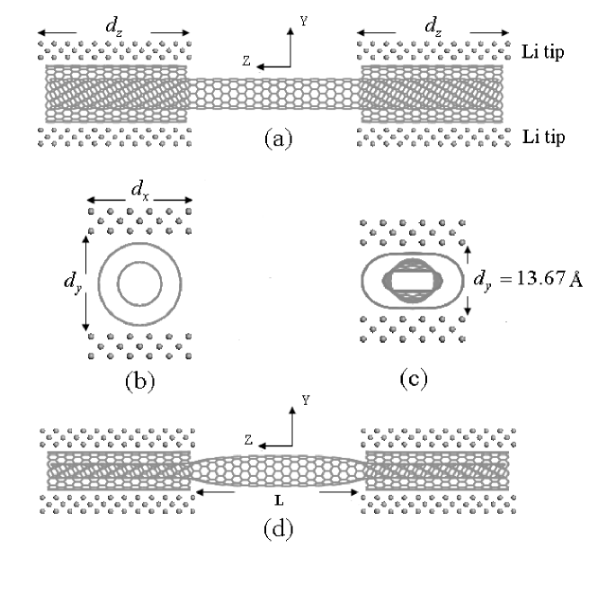
A finite DWNT (10,0)@(19,0) with a central segment of inner tube uncovered is shown schematically in Figs. 1(a) and 1(b), viewed from -axis and -axis direction, respectively. Two identical lithium tips (with definite width of and length of ) are applied from directions on the system with a separation distance . With the two tips moving towards the DWNT, the cross sections of the inner and outer tube are deformed from circle to ellipse, and finally to stadium-shaped shown in Figs. 1(c) and 1(d). Then the geometrical stucture of the DWNT for various tip distances are optimized by the universal force field (UFF) method [19,20]. When the deformation becomes bigger enough, the inner (10,0) tubes in the left DWNT and the right one will be able to exhibit a transition from semiconducting to metal. In this case, the original system will become a MSM DWNT IMJ, which has no any topological defects in the M-S and S-M junction region.
After the geometrical stucture of the DWNT IMJ is optimized, we will employ a TB Hamiltonian including four orbitals per atom to study its electronic and transport properties, in which the electron hybridization can be included [21,22,23]. The model Hamiltonian can be written as follows:
| (1) |
where and are the on-site energies of the 2 and 2 orbitals, respectively. and denote the annihilation (creation) operators of an electron on Carbon 2 orbitals at site and Carbon 2 orbitals at site , respectively. and are the orbital indices. are the hopping integrals between the orbital on the site and the orbital on the first or second-nearest neighbor site , which are expressed in terms of Slater-Koster parameters , , and [24]. Since the inter-wall interaction strength is about eighth of the intralayer hopping integrals, which has minor effect on the band structure of a DWNT [25], so we do not take it into account in this paper.
The parameter values in Eq. (1) are taken to be close to those used for graphite in Ref. [26], which was also successfully used to study the physical properties of the SWNT with small-radius [23], the SWNT with polygonized cross sections [21]. Among the four orbitals per atom, its level is located at eV below the triply-degenerated level taken as the zero of energy ( eV). The Slater-Koster hopping parameters for the nearest-neighbor pairs are taken as eV, eV, eV and eV. The second-neighbor interactions are taken into account by using eV, eV, eV and eV, where is a scaling factor, depending on the interatomic distance (in unit of Å).
First, we study the band structures of the radially deformed DWNT IMJ, and then, its transport properties . In the conductance calculation, the whole system is considered to be composed of two leads (left and right ones) plus a central DWNT IMJ (L-C-R), where the two leads are taken as the same type of the deformed metal inner tube (10,0) as those in the left and right deformed DWNT of the system. This problem can be most conveniently treated by the Green’s function matching method [27], in which the conductance is expressed by the Landauer formula:
| (2) |
where,
| (3) |
| (4) |
and
| (5) |
Here, is Hamiltonian of the central DWNT IMJ, and () is the coupling matrix between the central DWNT IMJ and the left (right) lead. and are the Green’s functions of the semi-infinite left and right leads, which are calculated by using an iterative procedure [28]. Also, we can calculate the local density of states (LDOS) by using LDOS, where is the ordinal number of carbon atoms in the DWNT IMJ.
III Results and Discussions
Based on the computational scheme, we optimized the geometrical structure of a finite DWNT (10,0)@(19,0) IMJ under the different tip distance . The obtained results show that small radial deformations generally cause elliptical cross sections for the DWNT. A further squashed deformation will lead the tubes to be flattened, producing a stadium-shaped cross section ( 13.67 Å, Fig. 1(c) and 1(d)), and meanwhile causing a semiconductor-to-metal transition (SMT) for the inner (10,0) tube of the DWNT. So, by using this model and the optimization procedure, we can get any of the MSM or semiconducting–metal–semiconducting (SMS) DWNT IMJ.
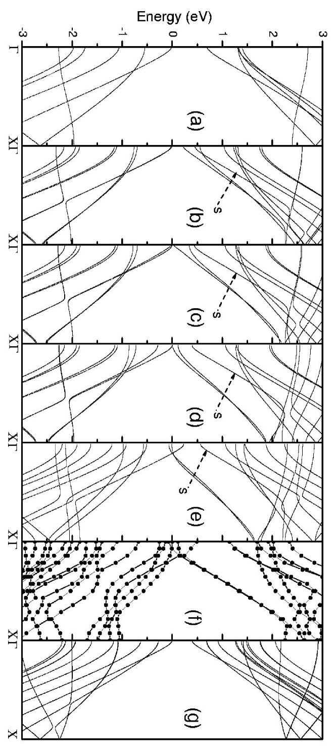
First, we study the electronic structure of the DWNT (10,0)@(19,0) IMJ. It is found that the outer tube (19,0) always remain in the semiconducting state when squashed (see Fig. 2(g)). But the band gap of the inner tube (10,0) decreases significantly from 0.69 eV to zero. Thus the squashed DWNT becomes an insulator-coated metallic wire. The obtained band structures for the perfect (10,0) tube and a series of deformed inner (10,0) tubes are shown in Figs. 2(a)-2(e). It can be seen from a comparison between Figs. 2(a) and 2(c) that when the tip distance decreases from 16.07 Å to 15.27 Å, the conduction band of the deformed (10,0) tube shifts down to the Fermi level and tends to split off, but the valence band is still similar to that of the perfect tube, accompanied by a very small energy split, which leads the energy gap to be reduced. Of special interest is that the non-degenerate state labeled by (s) in Fig. 2 moves down under radial deformation, which is caused by the enhanced hybridization, since the tube curvature is increased in the curved tube regions [20,21,22]. When the decreases to 14.47 Å, the gap is closed due to the lowest split conduction band touching the highest valence band, indicating a phase transition from semiconductor to metal (see Fig. 2(d)). Further squashing the DWNT ( 13.67 Å, Figs. 1(c) and 1(d)) will make the lowest split conduction band shift down deeper, leading to intercross of the original conduction and valence bands (see Fig. 2(e)), and meanwhile, all the bands near the Fermi level to be non-degenerate. In order to check the validity of the TB calculations, we have also carried out the first-principles calculation [29] on the deformed inner (10,0) tube with 13.67 Å. The obtained results (shown in Fig. 2(f)) indicate that, our TB calculations can correctly reproduce the first-principles results.
Next, we investigate the transport properties of the MSM DWNT IMJ by the above said method. Since the outer tube actually acts as an insulator coat of the inner metal wire, we do not take into account it in our transport calculation.
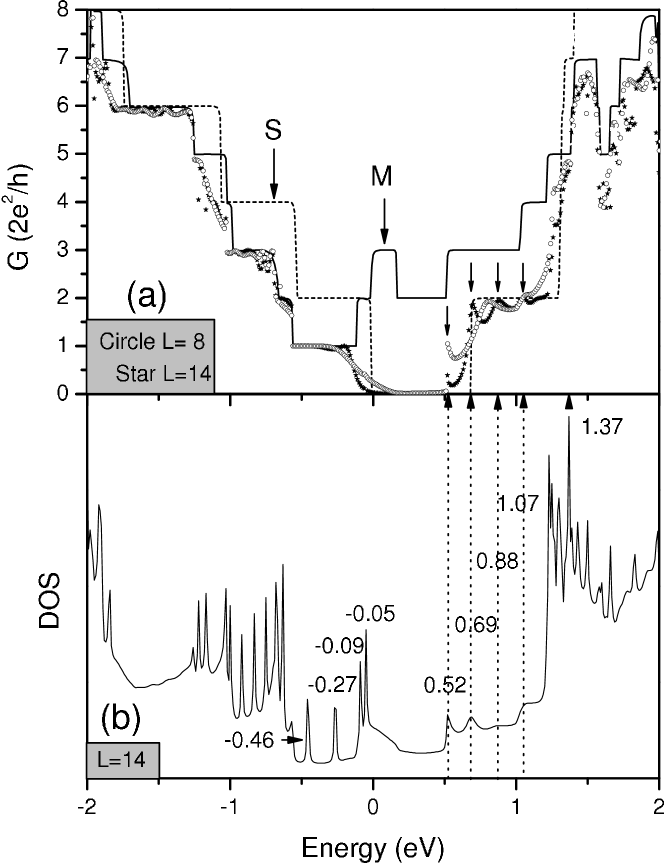
As is well known, the ballistic conductance at an energy level is proportional to the number of conduction channels at the same energy [30], from which the change of band structure may be clearly found by the conductance measurement. We have calculated the conductance and the total density of states (DOS) of the MSM DWNT IMJ with the central semiconductor length of 14 unit cell, and obtained results are given in Figs. 3(a) and 3(b). The calculated conductances of the perfect semiconducting (10,0) tube and the squashed metal (10,0) tubes ( 13.67 Å) are also shown in Fig. 3(a).
It is seen from Fig. 3(a) that radical squash induces the significant changes of the conductance near the Fermi level. And the conductances of the MSM DWNT IMJ below the Fermi level and above 1.37 eV are similar to those of deformed metal (10,0) tube. The biggest changes of the conductance appear in the energy window from 0 to 1.37 eV. Firstly, at 0.52 eV there is a conductance jump, which arises from the conductance jump of the squashed metal (10,0) tube at the 0.52 eV. Secondly, in the region of 0 0.69 eV (the band gap of the ideal (10,0) tube), there exists nonzero conductance, which comes from quantum tunnelling. Third, the resonance electron transmissions occur in the energy area of 0.69 1.37 eV, giving three conductance oscillation peaks at 0.69, 0.88 and 1.07 eV, respectively. Using a 1D square potential barrier with finite height, which is used to model the central semiconducting segment of the DWNT IMJ, we can simply get three oscillation peaks in their positions to be the same as those of the above three conductance peaks.
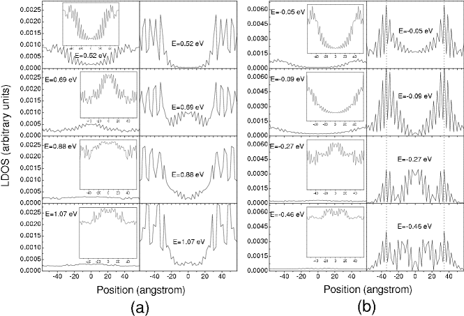
These interesting phenomena related to the conductance can be explained by the DOS shown in Fig. 3(b). From Fig. 3(b), we can see that there are four DOS peaks in the energy area of 0 1.37 eV, coinciding well with the four conductance peaks in the same energy window of Fig. 3(a). The LDOS along the tube axis at these four energy levels of 0.52, 0.69, 0.88 and 1.07 eV are shown in Fig. 4(a), it is clearly seen that all of the four states are extended along the tube axis. Also, the LDOS on the up surface of the MSM DWNT IMJ, shown in the left panel of Fig. 4(a), is much lower than that on the side surface, shown in the right panel, indicating that the conductances at these energy levels are contributed mostly by the atoms on the side surface [31]. In Fig. 4(b), we show the LDOS at four energy levels of -0.05, -0.09, -0.27 and -0.46 eV in valence band, respectively. The large contribution to conductance, coming from the atoms on the side surface of the MSM DWNT IMJ, can also be seen from Fig. 4(b). But we found that at energy levels of -0.05 and -0.09 eV exist the quasibound states with their largest LDOS at positions of Å (represented by the broken vertical lines) lying in the transition region between the deformed inner metal tube and the semiconductor tube. However, LDOSs at the energy levels of -0.27 and -0.46 eV show the characteristics of extended states.
In order to know effect of the length of central semiconducting part in the MSM DWNT IMJ, we have also calculated conductance of the IMJ with 8 unit cell and shown the obtained result in Fig. 3(a). For the transmission electrons, the middle semiconductor act as an energy barrier. And it is well known that the tunnelling probability decays exponentially with the increasing width of the energy barrier, which is well consistent with what shown in Fig. 3(a). Comparing with the conductance of the IMJ with 14 unit cell, we find the lower edge of the energy gap shifts to a higher energy, and a bigger conductance jump to (where is the conductance quantum) appears at 0.52 eV due to the stronger quantum tunnelling. And in the region of 0.69 1.37 eV, the resonance electron transmission peaks move to the higher energies.
Based on the MSM DWNT IMJ, we can easily make a pure carbon nanoscale transistor by applying a gate voltage to the DWNT junction with a inner semiconductor (10,0) tube. When 0, the conductance is zero and the transistor is OFF. With change of , the transistor can jump to an ON state.
IV Conclusion
In summary, based on Slater-Koster tight-binding and the first-principle calculations, we found that the different radically squashed DWMT IMJs have very different and hybridizations, inducing big changes of their electronic structures. It has been shown that the big enough radial squash can induce an insulator-metal transition for the inner semiconducting (10,0) tube, but the outer (19,0) tube remains to be semiconducting. The LDOSs of the MSM DWNT IMJ at different energies indicate the emergence of two quasibound states at -0.05 and -0.09 eV near the Fermi level, and large contributions to the conductance, coming from the atoms on the side surfaces of the IMJ. In addition, There exist several resonance conductance peaks at some energies in the conduction band of the MSM DWNT IMJ, which can be explained by electron resonance transmission effect. Also, the conductance variation due to length change of the central semiconducting part in the MSM DWNT IMJ has been found. Finally, a promising pure carbon nanoscale transistor is proposed based on the DWNT IMJ.
Acknowledgements.
We acknowledge discussions with Gang Wu. This work is supported by the Natural Science Foundation of China under Grants No. 90103038 and No. A040108.References
- (1) S. Iijima, Nature (London) 354, 56 (1991).
- (2) T.W. Ebbesen, P.M. Ajayan, Nature (London) 358, 220 (1992).
- (3) J. Kong, H.T. Soh, A.M. Cassell, C.F. Quate, H. Dai, Nature (London) 395, 878 (1998).
- (4) R. Saito, G. Dresselhaus, and M.S. Dresselhaus, Physical Properties of Carbon Nanotubes (Imperial College Press, London, 1998).
- (5) H.J. Dai, A.G. Rinzler, P. Nikolaev, A. Thess, D.T. Colbert, R.E. Smalley, Chem. Phys. Lett. 260, 471 (1996).
- (6) R. Saito, R. Matsuo, T. Kimura, G. Dresselhaus, M.S. Dresselhaus, Chem. Phys. Lett. 348, 187 (2001).
- (7) K. Tanaka, H. Aoki, H. Ago, T. Yamabe, K. Okahara, Carbon 35, 121 (1997).
- (8) Y.K. Kwon, D. Tomanek, Phys. Rev. B 58, R16001 (1998).
- (9) M. Buongiorno Nardelli, C. Brabec, A. Maiti, C. Roland, J. Bernholc, Phys. Rev. Lett. 80, 313 (1998).
- (10) T.W. Tombler, C. Zhou, L. Alexseyev, J. Kong, H. Dai, L. Liu, C.S. Jayanthi, M. Tang, and S. Wu, Nature (London) 405, 769 (2000).
- (11) E.D. Minot, Y. Yaish, V. Sazonova, J.Y. Park, M. Brink, and P.L. McEuen, Phys. Rev. Lett. 90, 156401 (2003).
- (12) J. Cao, Q.Wang, and H. Dai, Phys. Rev. Lett. 90, 157601 (2003).
- (13) A. Maiti, A. Svizhenko, and M.P. Anantram, Phys. Rev. Lett. 88, 126805 (2002).
- (14) M.B. Nardelli and J. Bernhole, Phys. Rev. B 60, R16338 (1999).
- (15) J.Q. Lu, J. Wu, W. Duan, F. Liu, B.F. Zhu, and B.L. Gu, Phys. Rev. Lett. 90, 156601 (2003).
- (16) J.Q. Lu, J. Wu, W. Duan, and B.L. Gu, arxiv:cond-mat/0312655.
- (17) Susumu Okada and Atsushi Oshiyama, Phys. Rev. Lett. 91, 216801 (2003).
- (18) Pingan Hu, Kai Xiao, Yunqi Liu, Gui Yu, Xianbao Wang, Lei Fu, Guanglei Cui, and Daoben Zhu, Appl. Phys. Lett. 84, 4932 (2004).
- (19) A.K. Rappe, C.J. Casewit, K.S. Colwell, W.A. Goddard, W.M. Skiff, J. Am. Chem. Soc. 114, 10024 (1992).
- (20) N. Yao, V. Lordi, J. Appl. Phys. 84, 1939 (1998).
- (21) J.C. Charlier, Ph. Lambin, and T. W. Ebbesen, Phys. Rev. B 54, 8377 (1996).
- (22) H.S. Sim, C.J. Park, and K. J. Chang, Phys. Rev. B 63, 073402 (2001).
- (23) X. Blase, L.X. Benedict, E.L. Shirley, and S. G. Louie, Phys. Rev. Lett. 72, 1878 (1994).
- (24) J.C. Slater and G.F. Koster, Phys. Rev. 94, 1498 (1954).
- (25) X.P. Yang, J.W. Chen, H. Jiang and J. Dong, Phys. Rev. B 69, 193401 (2004).
- (26) D. Tomanek and S.G. Louie, Phys. Rev. B 37, 8327 (1988).
- (27) M.B. Nardelli and J. Bernholc, Phys. Rev. B 60, 7828 (1999).
- (28) C. Caroli, R. Combescot, P. Nozieres, and D. Saint-James, J. Phys. C: Solid St. Phys. 4, 916 (1971).
- (29) M.D. Segall et al., J. Phys.: Cond. Matt. 14, 2717 (2002)
- (30) D.S. Fisher and P.A. Lee, Phys. Rev. B 23, 6851 (1981).
- (31) J.W. Chen, X.P. Yang, L.F. Yang, H.T. Yang and J. Dong, Phys. Lett. A 325, 149 (2004).
Figure Captions


