Spin configuration in a frustrated ferromagnetic/antiferromagnetic thin film system
Abstract
We have studied the magnetic configuration in ultrathin antiferromagnetic Mn films grown around monoatomic steps on an Fe(001) surface by spin-polarized scanning tunneling microscopy/spectroscopy and ab-initio-parametrized self-consistent real-space tight binding calculations in which the spin quantization axis is independent for each site thus allowing noncollinear magnetism. Mn grown on Fe(001) presents a layered antiferromagnetic structure. In the regions where the Mn films overgrows Fe steps the magnetization of the surface layer is reversed across the steps. Around these defects a frustration of the antiferromagnetic order occurs. Due to the weakened magnetic coupling at the central Mn layers, the amount of frustration is smaller than in Cr and the width of the wall induced by the step does not change with the thickness, at least for coverages up to seven monolayers.
1 Introduction
The interface of ferromagnetic and antiferromagnetic material is important from a scientific point of view because the competing ferromagnetic and antiferromagnetic interactions may lead to complex configurations particularly when there is frustration in the system. Especially when an antiferromagnetic layer is deposited on a ferromagnetic substrate with an atomic step (”hidden atomic step”) the magnetic frustration around this extended defect can give rise to interesting magnetic structures [1, 2, 3, 4]. Due to the localized nature of the frustrations, it has not been possible to resolve the spin configurations until the introduction of the Spin-Polarized Scanning Tunneling Microscopy/Spectroscopy (SP-STM/STS) [5].
This problem is also important from the technological point of view. Exchange bias is one of the phenomena associated with the exchange anisotropy created at the interface between an antiferromagnetic material and a ferromagnetic material. Materials exhibiting exchange bias have been used in several practical applications since their discovery [6, 7, 8]. In the world of magnetic devices, the goal is to get smaller. The smaller space one bit of information can occupy, the more data you can get into a device. Between two magnetic domains with opposite magnetization directions always exists a domain wall. Therefore a deep understanding of the parameters that control the domain wall width are crucial in order to achieve higher density for data storage.
Mn is exactly in the middle of the 3 transition metal series, just between Fe, which is a natural ferromagnet in the bulk, and Cr, which is an antiferromagnet. Therefore, Mn stands as one of the more complex 3 transition metals from the point of view of the magnetic coupling, and it is a clear candidate to exhibit a great variety of magnetic structures. Mn systems have been experimentally investigated by spin-polarized electron energy loss spectroscopy [9], scanning electron microscopy with polarization analysis [10] and SP-STM/STS [11, 12]. A layered antiferromagnetic (LAF) arrangement was found in the Mn film. Recently, part of the authors [13] have studied the same system using the ab-initio tight-binding linear muffin-tin orbitals (TB-LMTO) method [14], assuming the experimental interlayer distances and a magnetic arrangement at the surface as experimentally observed [11]. Different magnetic solutions with energy differences of few meV were obtained, with the LAF configuration the less energetic state, in good agreement with the experiments. The LAF as well as the closest metastable solutions had some common features: i) parallel coupling at the interface between Mn and Fe, ii) antiparallel coupling between the Mn-surface and subsurface layers and iii) antiparallel coupling between the two Mn layers closest to the interface. This set of solutions only differ in the couplings at the central Mn layers, that were parallel or antiparallel depending on the Mn thickness, which make these systems clear candidates to exhibit noncollinear magnetic arrangements under structural defects like monoatomic steps. Theoretically, Hafner and Spišák [15] have found complex magnetic coupling in Mn films on Fe(001) allowing atomic relaxations, obtaining an in-plane antiferromagnetic structure.
In this paper, the magnetic structure of thin Mn films grown on Fe(001) is studied. In particular, we focus our attention at the magnetic structure of the Mn films around steps on the Fe(001) substrate. In Section 2, by means of SP-STM/STS, we measure in real space and with high spatial resolution the magnetic structure of the films around these defects. The experimental results are interpreted, in Section 3, with the help of ab-initio-parametrized self-consistent real-space tight binding (TB) calculations in which the spin quantization axis is independent for each site thus allowing noncollinear magnetism. Throughout the paper, comparisons are made with the Cr/Fe(001) system to get a deeper understanding of which material parameters are crucial to determine the resulting magnetic structure. Finally, in Sec. 4 we summarize our conclusions.
2 Experimental results
All measurements were performed in an ultra-high vacuum (UHV) chamber ( mbar) at room temperature (RT). An STM was attached to the chamber, which is equipped with molecular beam epitaxy, Auger spectroscopy, field emission spectroscopy, sample heating and sputtering facilities [11]. W tips were cleaned by Ar sputtering and annealing and then covered with 10 nm Fe. SP-STS measurements were performed in two different ways: In the first one, curves were obtained at every pixel of a constant current topographic image and then numerically differentiated. In the second one, maps were obtained with a lock-in amplifier modulating the sample bias voltage by 40mV at 2 kHz.
The growth conditions are very important because Mn and Fe tend to intermix and the magnetic properties of the Mn are very sensitive to the atomic structure [16]. In this work, Mn was grown on the Fe(001) whisker at 100 C at a rate of 0.6nm/min, and the surface topography and electronic structure was characterize by means of scanning tunneling microscopy/spectroscopy (STM/STS) at RT in UHV using a clean W tip. Atomically and chemically resolved STM images show that the Mn film grows with the same in-plane lattice constant as Fe(001) and that the Fe atoms intermix with the first, the second, and the third Mn layer. The concentration of intermixed Fe decreased with film thickness. Furthermore, STM shows that the growth mode changes from layer-by-layer to layer-plus-islands for coverages higher than 4 ML of Mn. If the temperature of the substrate is increased by few degrees, this transition from layer-by-layer to layer-plus-islands takes place for thicker Mn layers and the intermixed Fe is present in more Mn layers. Based on apparent step height measurements, done choosing the bias voltage carefully to avoid the influence of the electronic structure on the results, we conclude that the first two Mn overlayers show a significant higher step heights than the Fe single step and that the Mn film relaxes by about 0.02 nm at the third layer. From the fourth layer the interlayer spacings are geometrically the same (about 0.165 nm) and the structure is a body-centered tetragonal structure [17]. This bct Mn(001) has a layered antiferromagnetic arrangement [10, 11].
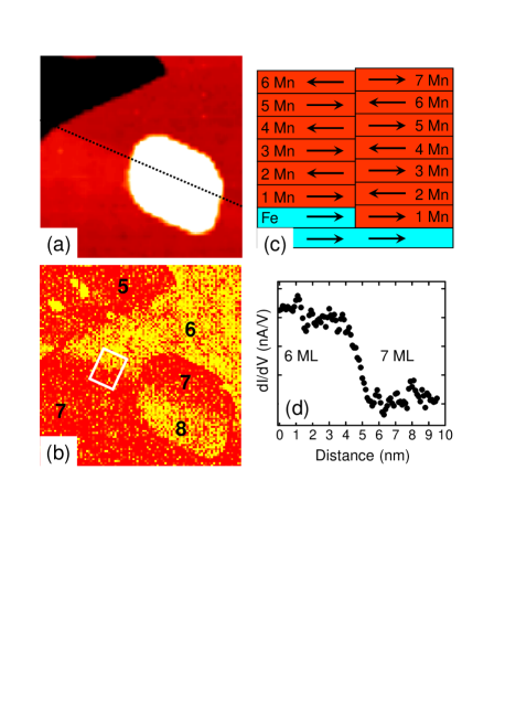
When a Mn film is grown across an Fe step (hidden), the Mn film tends to produce a flat surface. We always find steps 0.02 nm high, that corresponds to the difference between the interlayer distances for Fe and Mn. Across one of these steps, the Mn thickness changes by one layer (see of Fig. 1(c)). Due to the LAF structure, the magnetization of the surface layer is reversed across these steps. maps obtained with clean W tips around these defects show the same electronic structure on both sides. However, when using Fe covered W tips, contrast of magnetic origin is obtained across the hidden step as can be seen in Fig. 1(b). The average profile measured in the white box shown in panel (b) can be seen in panel (d) and gives a domain wall width of around 1.16 nm (2-4 lattice parameters).
To study the possible influence of the set-point values on the observed domain width, we changed systematically the set point voltage and set point current. Firstly, the set point currents were varied with fixed set point voltage, so with varying tip-sample distance (Fig. 2(a)). In addition, the set point voltage and current were varied such that the tunneling resistance stayed constant, so with approximately constant tip-sample separation (Fig. 2(b)). From the results given in Fig. 2(a) and 2(b), we can conclude that our values for the domain wall width do not depend on the particular set-point used.
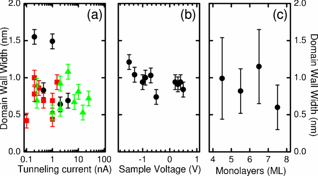
In Fig. 2(c) we show the result of 40 measurements taken with 6 different magnetic tips for hidden steps covered by different Mn thicknesses. There is no clear dependence between the width of the domain wall and the thickness of the Mn film in the range explored. The error bars in these measurements simply reflect the fact that the tips are different and the resolution of the magnetic images is affected.
3 Theoretical results
For the theoretical investigation of our samples, it is important to point out that when defects are present like in this system, with the consequent lack of symmetry and hundreds of inequivalent sites, real space methods with reasonable computer requirements are demanded. We have employed an ab-initio-parametrized self-consistent real-space tight-binding method in which the spin quantization axis is independent for each site thus allowing noncollinear magnetism. This method has been recently developed and used satisfactory for the study of supported Cr films on Fe substrates with monoatomic steps [18]. The Hamiltonian in our method can be split into a band term and an exchange term , which in the orthogonal basis of atomic site and orbital and with the usual notation are:
| (3) | |||
| (6) |
contains both the non-diagonal matrix elements (hopping integrals, , between orbitals and of different sites and , which are assumed to be spin independent) and the spin-independent part of the diagonal matrix elements (), being the sum of the local level , the electrostatic level shift accounting for the charge variations parameterized by the Coulomb integral and the crystal field potential , where is the local atomic coordination of site . describes the magnetic part, through the exchange parameter multiplied by the magnitude of the local magnetic moment, , whose direction is given by the angles in the spin-rotation matrix. The spin-orbit contribution is not considered here. The Hamiltonian has been parametrized to DFT TB-LMTO calculations of thin Mn films supported on ideal Fe(001) [13] in order to take into account the effects of surface, interface and bulk.The transferability of the parametrization has been checked in systems of 6 and 7 Mn ML on Fe(001), comparing the results with those obtained with the TB-LMTO method [13], finding similar values for the energy differences and magnetic moments.
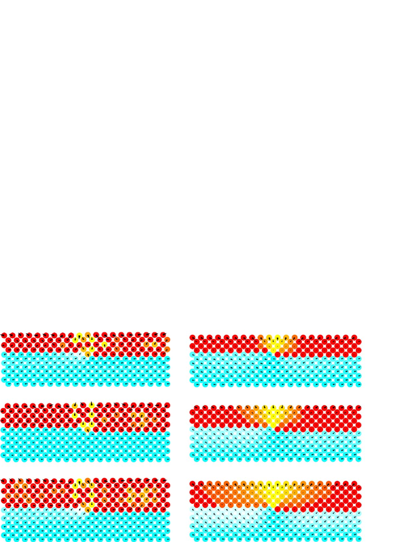
We have simulated the systems represented in Fig. 1. Despite the fact of preserving the symmetry in the axis parallel to the step, that can be justified by the length of the observed steps in the system, we have about 40000 atoms and up to 600 inequivalent sites to describe the semi-infinite system. We have considered coverages of 4-5, 5-6 and 6-7 Mn ML. In all cases, a small step of about 0.02 nm at the surface is present (as experimentally observed). In Fig. 3 (left panel) we illustrate the noncollinear magnetic moment distributions obtained in the calculations (only a portion of the semi-infinite system is shown). To understand the origin of the noncollinear magnetic arrangement, we have also performed TB collinear restricted calculations (not shown), obtaining different magnetic arrangements, the least energetic one displaying the LAF order at both sides far from the step, while just over the step, due to the impossibility to reach in the whole system the LAF order together with the parallel coupling at the interface, magnetically frustrated atoms were present. Previous studies in Cr/Fe interfaces with steps [18] have shown that this type of frustrations in the collinear framework lead the system to drastically reduce the magnetic moments in the frustrated region. However, this moment reduction in the case of Mn is much less noticeable, which is consistent with the fact that the magnetic couplings between Mn layers are weaker and less defined than in Cr for which the LAF solution is the only one present [18]. The noncollinear magnetic solutions shown in Fig. 3 are energetically more stable than the collinear ones in all cases and reproduce the experimentally observed magnetic contrast at the surface between both sides of the step. This is due to the propagation of the magnetic frustration originated at the interface step. Far from the step, the system tends to preserve the magnetic couplings found in the ideal Mn films on Fe(001) [13], that is the LAF with parallel Fe-Mn coupling at the interface and antiparallel coupling between Mn surface and subsurface layers. Moreover, the tendency of Mn to couple both parallel and antiparallel in the central layers of the ideal Mn films on Fe(001) is also reflected in the noncollinear arrangements shown in Fig. 3
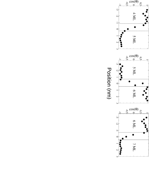
Let us now come to the analysis of the domain-wall evolution as a function of the Mn coverage, in particular the width of the domain-wall. Experimentally, we have found a domain-wall width of about 2-4 lattice parameters independently of the Mn coverage. Our theoretical results (Fig. 3) are also consistent with the experimental finding, as it can be deduced from Figs. 4 and 5 where the cosine of the angle of the local surface magnetic moment with respect to the bulk are plotted through the step (red squares). The central Mn layers decouple the surface from the interface in a large extent, and make these systems to behave in a radical different way from what would be expected if one assumes for Mn the magnetic coupling of a typical antiferromagnet like Cr and the associated magnetic frustrations when interfaced with stepped Fe. In fact, we have already indicated before that Mn and Cr have different magnetic behavior when deposited on an atomically flat Fe(001) surface. The magnetic decoupling of the surface layers from the deeper layers coupled to the substrate has been also proposed recently by Hafner and Spišák [15]. This provides further support to our results. For coverages larger enough it is expected that Mn will undergo structural transition [19] with no magnetic domains at the surface. Our results contrast, however, with those obtained by Schlickum et al. [12]. These authors found an increase of the domain-wall width as increasing Mn coverage. Growth conditions are very important for the final structure. In these experiments we grew the Mn films about ten times faster than Schlickum et al. [12]. The faster deposition rate for the same sample temperature may lead to a smaller level of intermixing between Mn and Fe and therefore to a different magnetic structure. Furthermore Schlickum et al. [12] explained their results using a simple Heisenberg model for localized magnetism [12] assuming that Mn behaves like Cr and considering the same exchange parameter for Mn-Fe and Mn-Mn.
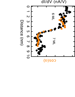
In order to further illustrate the different magnetic behavior of Mn and Cr, we have performed the same type of calculations in similar systems, but with Cr instead of Mn deposited on the stepped Fe substrate and the corresponding interatomic distances (Fig. 3, right panel). The difference between the noncollinear arrangements in Mn/Fe and Cr/Fe is clear. The strong antiferromagnetic character of Cr leads to strong magnetic frustrations that are propagated towards the surface occupying a region in which the best compromise to the antiparallel Cr-Cr and Cr-Fe couplings is achieved. As a result, the domain-wall width increases with increasing Cr coverage and the frustration is partially released in the Fe(001) substrate.
4 Conclusions
In conclusion, we have investigated the magnetic structure on thin Mn films grown on a Fe(001) surface with a monoatomic step. In our SP-STM images we found a change in the magnetic contrast when crossing one of those steps due to the change of the Mn thickness. We have found that the width of the domain wall around the substrate steps does not depend on the thickness, at least for coverages up to 7 Mn overlayers, and it is about 2 lattice parameters. This is due to the weakly defined magnetic coupling at the central Mn layers that decouple the surface from the interface in a large extent. We compare our findings for the Mn films with the behavior of Cr films. In contrast to Mn, ideal Cr films have strong antiferromagnetic couplings and larger range order than in Mn, up to the point that only one magnetic arrangement in the system has been found in the collinear framework, corresponding to a LAF configuration. This strong coupling produces a high amount of frustration on steps and as a consequence in the case of Cr the domain wall width increases with the coverage.
Financial support by the Ministerio de Ciencia y Tecnología and Ministerio de Educación y Ciencia through project numbers FIS2004-01206 and MAT2005-03415, Junta de Castilla y León (VA068A06) and INTAS (03-51-4778) is gratefully acknowledge. HvK thanks Instituto Universitario ”Nicolás Cabrera” for a visitors grant.
References
References
- [1] Berger A and Hopster H 1994 Phys. Rev. Lett. 73 193
- [2] Vega A, Demangeat C, Dreyssé H and Chouairi A 1995 Phys. Rev. B 51 11546
- [3] Stoeffler D and Gautier F 1995 J. Magn. Magn. Mater. 147 260
- [4] Berger A and Fullerton E E 1997 J. Magn. Magn. Mater. 165 471
- [5] Bode M, Getzlaff M and Wiesendanger R 1998 Phys. Rev. Lett. 81 4256
- [6] Prinz G A 1998 Science 282 1660
- [7] Nogus J and Schuller I K 1999 J. Magn. Magn. Mater. 192 203
- [8] Wolf S A, Awschalom D D, Buhrman R A, Daughton J M, von Molnar S, Roukes M L, Chtchelkanova A Y and Treger D M 2001 Science 294 1488
- [9] Walker T G and Hopster H 1993 Phys. Rev. B 48 3563
- [10] Tulchinsky D A, Unguris J and Celotta R J 2000 J. Magn. Magn. Mat. 212 91
- [11] Yamada T K, Bischoff M M J, Heijnen G M M, Mizoguchi T and van Kempen H 2003 Phys. Rev. Lett. 90, 056803
- [12] Schlickum U, Janke-Gilman N, Wulfhekel W and Kirschner J 2004 Phys. Rev. Lett. 92 107203; Wulfhekel W, Schlickum U and Kirschner J 2005 Micros. Res. and Tech. 66 105
- [13] Martínez E, Vega A, Robles R and Vázquez de Parga A L 2005 Phys. Lett. A 337 469
- [14] Andersen O K and Jepsen O 1984 Phys. Rev. Lett. 53 2571
- [15] Hafner J and Spišák D 2005 Phys. Rev. B 72 144420
- [16] Wu R and Freeman A J 1996 J. Magn. Magn. Mater. 161 89
- [17] Yamada T K, Bischoff M M J, Mizoguchi T and van Kempen H 2002 Surf. Sci. 516 179
- [18] Robles R, Mart\a’ınez E, Stoeffler D and Vega A 2003 Phys. Rev. B 68 094413
- [19] Passamani E C, Croonenborghs B, Degroote B and Vantomme A 2003 Phys. Rev. B 67 174424