Optical properties of SiC nanotubes: A systematic ab initio study
Abstract
The band structure and optical dielectric function of single-walled zigzag (3,0),(4,0),(5,0),(6,0),(8,0),(9,0),(12,0),(16,0),(20,0),(24,0), armchair (3,3),(4,4),(5,5),(8,8),(12,12),(15,15), and chiral (4,2),(6,2),(8,4),(10,4) SiC-NTs as well as the single honeycomb SiC sheet have been calculated within density functional theory with the local density approximation. The underlying atomic structure of the SiC-NTs is determined theoretically. It is found that all the SiC nanotubes are semiconductors, except the ultrasmall (3,0) and (4,0) zigzag tubes which are metallic. Furthermore, the band gap of the zigzag SiC-NTs which is direct, may be reduced from that of the SiC sheet to zero by reducing the diameter (), though the band gap for all the SiC nanotubes with a diameter larger than 20 Å is almost independent of diameter. For the electric field parallel to the tube axis (), the for all the SiC-NTs with a moderate diameter (say, 8 Å) in the low-energy region (06 eV) consists of a single distinct peak at 3 eV. However, for the small diameter SiC nanotubes such as the (4,2),(4,4) SiC-NTs, the spectrum does deviate markedly from this general behavior. In the high-energy region (from 6 eV upwards), the for all the SiC-NTs exhibit a broad peak centered at 7 eV. For the electric field perpendicular to the tube axis (), the spectrum of all the SiC-NTs except the (4,4), (3,0) and (4,0) nanotubes, in the low energy region also consists of a pronounced peak at around 3 eV whilst in the high-energy region is roughly made up of a broad hump starting from 6 eV. The magnitude of the peaks is in general about half of the magnitude of the corresponding ones for . Interestingly, the calculated static dielectric constant for all the SiC nanotubes is nearly independent of diameter and chirality with for being only about 30 % larger than for . The calculated electron energy loss spectra of all the SiC nanotubes for both electric field polarizations are rather similar to that of of the SiC sheet, being dominated by a broad -electron plasmon peak at near 21 eV and a small -electron plasmon peak at 3 eV.
pacs:
71.20.Tx, 73.22.-f, 78.67.Ch, 78.67.-nI INTRODUCTION
Since their discovery in 1991 Iijima , carbon nanotubes (CNTs) have attracted considerable interest worldwide because of their unusual properties and great potentials for technological applications. CNTs can be regarded as a layer of graphene sheet rolled up in a tubular form Saito , and the structure of a CNT is specified by a chiral vector defined by a pair of integers (). CNTs can be chiral or nonchiral depending on the way they are rolled up. Their physical properties, in particular, optical dielectric functions, depend sensitively on their chirality, i.e., the () indices (see, e.g., Ref. Chu, ; Guo, and references therein). Apart from CNTs, inorganic tubular materials, such as BN Lin ; Rubio , AlN Mei , GaN Lee , have also been predicted and synthesized. These tubular materials also display some very interesting properties distinctly different from their bulks.
Bulk silicon carbide (SiC) crystallizes in either a cubic or a hexagonal form, and exbihits polytypism mun82 ; wyc63 . The polytypes are made of identical hexagonal layers with different stacking sequences. These polytypes are semiconductors with a range of band gaps, from 2.39 eV in the zincblende (3C) to 3.33 eV in the wurtzite polytype (2H) mun82 ; iva92 . Furthermore, 3C and 6H SiC are used for high temperature, high-power and high-frequency devices C ; Wang ; Rurali ; Park due to their unique properties SiC , while 6H SiC with a band gap of 2.86 eV is a useful material for blue light-emitting diode applications iva92 . Recently, SiC-NTs were also synthesized by the reaction of CNTs and SiO at different temperature sun02 . This has stimulated a number of both theoretical and experimental investigations on the tubular form of the SiC pei06 ; Pei ; Menon ; Xia ; Mavrandonakis . Based on density-functional calculations, Miyamoto and Yu Miyamoto predicted the existence of graphitic and tubular forms of SiC and also proposed their synthesis using an extreme hole injection technique. They also reported that the strain energies of SiC-NTs are lower than that of CNTs, and that the band gaps of SiC-NTs can be direct or indirect, depending on the chirality. Using both tight-binding molecular dynamics and ab initio methods, Menon and coworkers Menon showed that single-walled SiC-NTs are highly stable with a large band gap. Zhao et al. Zhao also investigated theoretically the strain energy, atomic and electronic structure of SiC-NTs with or without hydrogenation. Gali performed an ab initio study of the effect of nitrogen and boron impurities on the band structure of the SiC-NTs Gali .
Unlike CNTs, SiC-NTs are polar materials and therefore, may exhibit some unusual physical properties that CNTs may not have. For example, zigzag SiC-NTs may become piezoelectric, and also show second-order non-linear optical response. Despite the intensive theoretical studies mentioned above, no ab initio calculation of the dielectric response and optical properties of SiC-NTs has been reported, perhaps because of the heavy demand on computer resources. A knowledge of the optical properties of SiC-NTs is important for their optical and electrooptical applications. The primary objective of this work is to analyze the band structure and optical characteristics of all three types of the SiCNTs by ab initio calculations. This will help to distinguish the electronic and optical properties of CNTs and BN-NTs from that of SiC-NTs. Our ab initio calculations are also needed to help understand the existing and future optical experiments.
This paper is organized as follows. In the next Sec., the theoretical approach and computational method are described. In Sec. III, the band structure, density of states (DOS), electron energy loss spectra (EELS), optical dielectric function of the single SiC sheet and SiC-NTs are discussed. Finally, conclusions are given in Sec. IV.
II Theory and computational method
Our ab initio calculations for the SiC-NTs are performed using the accurate full-potential projector augmented wave (PAW) method blo94 , as implemented in the VASP package. kre94 They are based on density-functional theory (DFT) with the local-density approximation (LDA). The supercell method is used such that the identical SiC tubes are aligned in a square array and the closest interwall distance between the adjacent tubes is at least 10 Å. We consider a number of the SiC-NTs with different diameters and chirality () from all three types, as listed in Table I.
First, the ideal SiC-NTs are constructed by rolling up a graphitic hexagonal SiC sheet. The atomic positions and lattice contants were then fully relaxed by the conjugate gradient (CG) method. The theoretical equalibrium atomic positions and lattice constant were obtained when the forces acting on all the atoms and the axial stress are less than 0.04 eV/Å and 1.0 kBar, respectively. In these atomic position optimizations, a uniform grid (11n) along the nanotube axis (-axis) with the number of the -points being from 30 to 50. The special -point method and the Gaussian broadening technique were used for the Brillouin zone (BZ) integration. The length of theoretical translational vector T and theoretical diameter D are listed in Table I. The curvature energy (total energy relative to that of single SiC sheet) (also known as the strain energy) of the SiC-NTs is listed in Table II. Note that for the nanotubes with a moderate diameter ( Å), the equilibrium structures are already found to be almost the same as that of the ideal nanotubes constructed by rolling-up a SiC sheet with a Si-C bondlength of 1.771 Å. This is consistent with the fact that the calculated of the nanotubes with such a diameter is already smaller than 0.05 eV/atom (Table II). Interestingly, like CNTs and BN-NTs, the calculated of the SiC-NTs can be very well fitted with with = 2.004 eVÅ2/atom, indicating that the conventional elastic theory works well even down to such a small length scale. for the SiC-NTs is identical to that of the CNTs but larger than that (1.248 eV Å2/atom) of the BN-NTs calculated previously using the same band structure method Lin . However, of 1.75 eV Å2/atom reported in Ref. Zhao, is somewhat smaller than the present calculations.
| (Å) | (Å) | ||
|---|---|---|---|
| (3,3) | 5.05 | 3.08 | 12 |
| (4,4) | 7.43 | 3.08 | 16 |
| (5,5) | 8.45 | 3.07 | 20 |
| (8,8) | 13.49 | 3.07 | 32 |
| (12,12) | 20.25 | 3.07 | 48 |
| (15,15) | 25.35 | 3.07 | 60 |
| (3,0) | 3.36 | 5.14 | 12 |
| (4,0) | 4.13 | 5.22 | 16 |
| (5,0) | 5.10 | 5.25 | 20 |
| (6,0) | 6.06 | 5.26 | 24 |
| (8,0) | 7.89 | 5.29 | 32 |
| (9,0) | 8.89 | 5.3 | 36 |
| (12,0) | 11.82 | 5.3 | 48 |
| (16,0) | 15.61 | 5.3 | 64 |
| (20,0) | 19.85 | 5.4 | 80 |
| (24,0) | 23.48 | 5.3 | 96 |
| (4,2) | 5.25 | 14.28 | 56 |
| (6,2) | 7.16 | 19.5 | 104 |
| (8,4) | 10.5 | 14.03 | 112 |
| (10,4) | 12.17 | 11.06 | 104 |
The final self-consistent electronic structure calculations were then performed on the theoretically determined structures of the SiC-NTs. In the self-consistent electronic structure calculations, the number n of the -points along the -axis used ranges from 40 to 50. The density of states (DOS) was evaluated from the final band structures by Gaussian broadening method:
| (1) |
where the Dirac delta function is approximated by the Gaussian function,
| (2) |
is the weight associated with -point k, and is the th energy band. Here the Gaussian width is set to 0.04 eV. An denser -point grid along the z-axis with n ranging from 40 to 100 was used for the DOS calculations.
The optical properties were calculated based on the independent-particle approximation, i.e., the quasi-particle self-energy corrections, the local-field corrections and the excitonic effects were neglected. In particular, the band gap of SiC in the wurtzite (2H) structure from our LDA calculations is 2.15 eV, being 1.18 eV smaller than the experimental value mun82 ; iva92 . This suggests that the quasi-particle self-energy corrections to the optical peak positions may amount to 1 eV in the SiC systems. Furthermore, because the LDA underestimates the energy gaps, the calculated dielectric function would be slightly too large in general. For example, our calculated dielectric function at 0 eV for the electric field parallel and perpendicular to the -axis of 2H SiC is 8.33 and 7.90, respectively, being slightly larger than the corresponding measured , 6.84 and 6.51. mun82 Therefore, the results from the present LDA-independent-particle calculations should not be quantitatively compared with experiments, though they would certainly be useful to study the trends and characteristics of the optical properties of the SiC-NTs. Nonetheless, our previous calculations show that the dielectric functions of graphite Chu and also of h-BN Lin calculated within the independent-particle picture are in reasonable agreement with experiments, perhaps because of the accidental cancellation of the self-energy corrections by the excitonic effects.
The imaginary part of the dielectric function () is given by the Fermi golden rule (see, e.g., Ref. Chu, ) (atomic units are used in this paper), i.e.,
| (3) |
where is the photon energy and is the unit cell volume. The dipole transition matrix elements = were obtained from the final self-consistent band structure with the PAW formalism. ado01 VB and CB denote the valence and conduction bands, respectively. The represents the th Bloch state wave function with crystal momentum k, and a represents the Cartesian component. We can obtain the real part of the dielectric function by the Kramer-Kronig transformation,
| (4) |
where P denotes the principal value of the integral. Given the complex dielectric function +i, all other linear optical properties such as reflectivity, refraction index, and absorption spectrum can be calculated. The electron energy loss spectra at the long wavelength limit is given by . The electric polarizability is defined by =1+4/.
In the present calculations, the -function in Eq. (3) is approximated by Gaussian function Eq. (2) with eV. The same -point grid as in the DOS calculations is used. As noticed before Chu ; Lin , the unit cell volume is not well defined for nanotubes. Therefore, as in previous calculations Chu ; Lin , we used the effective unit cell volume for the SiC-NTs instead of the volume of the supercells, which is arbitrary. The effective unit cell for a nanotube is given by , where d is the thickness of the SiC-NT cylinder which is set to the interlayer distance of h-SiC (3.51 Å). Although the value of the effective unit cell volume used may change the magnitude of the dielectric functions as can be seen from Eq. (3), it would not affect the energy positions and shapes in the dielectric functions.
III RESULTS AND DISCUSSION
III.1 Single SiC sheet
In order to understand the calculated properties of the SiC-NTs, we have also calculated the self-consistent electronic band structure and dielectric function for an isolated honeycomb SiC sheet. The isolated SiC sheet is simulated by a slab-supercell approach with an intersheet distance of about 10 Å. The underlying structure was determined theoretically by using a -mesh of , and the theoretical lattice constant is Å.
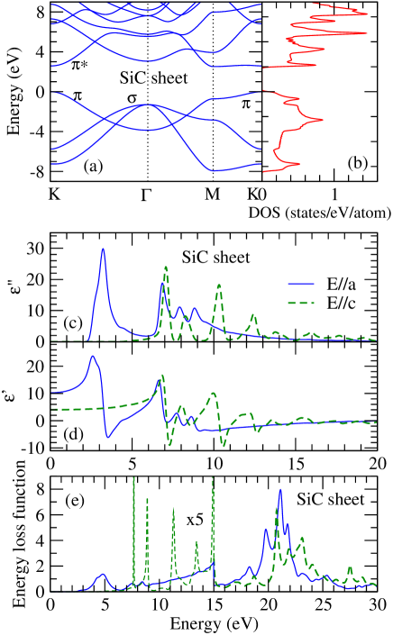
The calculated band structure and density of states for the isolated SiC sheet are displayed in Fig. 1. Clearly, the SiC sheet is a semiconductor with a direct band gap of 2.58 eV. The top of valence bands and the bottom of conduction bands both occur at symmtry point K in the hexagonal Brillouin zone. Both the upper valence band and the lower conduction band are predominantly of Si and C p-orbital character. The upper valence band consists of one band which arises from the and orbitals, extending above and below the SiC layer plane, and two bands involving the three Si 2, , and three C 3, , orbitals, which form the coplanar Si-C bonds. The low-lying conduction bands ranging from 2.4 eV to 5.6 eV are predominantly of the character, indicating that they are the bands. These electrons play an essential role for electrical conductivity.
The calculated dielectric function () of the SiC sheet is displayed in Fig. 1. In our calculations, a dense -point grid of 60601 is used. The optical properties of the single SiC sheet can be roughly divided into two spectral region. In the low-energy range from 2 to 6 eV, the interband optical transitions involve mainly the bands. At higher energies, the optical absorption peaks between 6 to 11 eV are associated with the interband transitions involving bands. Strong anisotropy in the optical spectra is expected due to distinct optical selection rules, as can be seen from Fig. 1. For a single SiC sheet, only and transitions are allowed if the electric field is polarized parallel to the SiC-layer plane (). In contrast, only and transitions are allowed if the is polarized perpendicular to the SiC-layer plane (). This explains why there is a strong absorption peak at 3.0 eV for () in the single SiC sheet [Fig. 1(c)]. For the single SiC sheet, there is no optical absorption for below 5 eV (Fig. 1c).
The calculated electron energy loss spectra (EELS) of the SiC sheet are shown in Fig. 1e. For , two prominent peaks are found in the energy loss function, (Fig. 1e). A small one at 5 eV may be attributed to the collective excitation of electrons partially screened by the electrons. A large broad resonance (actually, a multi-peak manifold) near 21.0 eV is associated with plasma oscillations involving both the and electrons. For , there is also a broad resonance in the high energy region, but at around 23.5 eV. However, there is no distinct peak at 5 eV. There are instead many spiky thin peaks in the low energy region from 7 to 15 eV (Fig. 1e).
III.2 Band structure of the SiC nanotubes
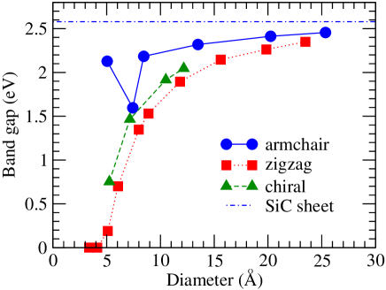
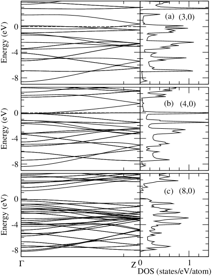
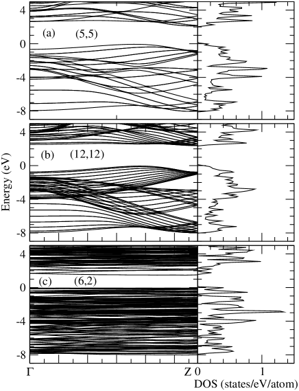
The calculated band gaps of all the SiC-NTs are listed in Table II and also displayed as a function of the tube diameter in Fig. 2. The band structures of the selected zigzag, armchair and chiral SiC-NTs are shown in Figs. 3 and 4. All the SiC-NTs, with the exceptions of the ultrasmall (3,0) and (4,0) nanotubes, are semiconductors. In particular, all the semiconducting zigzag SiC-NTs have a direct band gap (Table II and Fig. 3). The top of valence bands and the bottom of the conductions both occur at the center () of the 1D Brillouin zone. This suggests that the zigzag SiC-NTs may find applications in optical and opto-electronic devices such as SiC lasers. Interestingly, the ultrasmall diameter zigzag (3,0) and (4,0) tubes are metallic (Fig. 3a-b and Table II). The (3,0) nanotube has a light electron pocket at Z with an effective mass of 0.27 and two doubly degenerate heavy hole pockets at with an effective mass of 1.0. The (4,0) nanotube has a light electron pocket at with an effective mass of 0.51 and two doubly degenerate heavy hole pockets at Z with an effective mass of 1.42. They could be the smallest SiC metallic nanowires and may have applications in nano-electronics and high efficient field emissions. Nevertheless, since the LDA underestimates the band gap, this prediction of metallic (3,0) and (4,0) zigzag SiC nanotubes should be treated with caution. In contrast, all the armchair and chiral SiC-NTs are indirect band gap semiconductors (see Table II and Figs. 4). For the armchair SiC-NTs, the bottom of conduction bands generally appears at the 1D Brillouin zone boundary (Z), while the top of valence bands occurs at somewhere between the and Z points (Fig. 4).
Fig. 2 shows that the band gap of the small SiC-NTs increases with diameter, and approaches the band gap of the isolated SiC-sheet as the diameter becomes larger than 20 Å. The reduction of the band gap in the small diameter SiC-NTs may be attributed to the curvature effects Okada . When a SiC sheet is rolled up to form a SiC-NT, the and orbitals are no longer orthogonal to each other, and can hybridize. The hybridization of the and orbitals would modify the band structures of the SiC-NTs obtained by rolling up a SiC-sheet. Remarkably, the reduction of the band gaps of the zigzag SiC-NTs is monotonic and very large such that the ultrasmall (3,0) and (4,0) zigzag tubes become metallic (Fig. 2). This strong diameter dependence of the band gap can perhaps be used to engineer the band gap of the SiC-NTs by growing the tubes with a prespecified diameter. Nonetheless, the reduction of the band gap of the armchair SiC-NTs is much smaller (within 0.5 eV), except the (4,4) SiC-NT (Fig. 2). The reduction of the band gap for the chiral SiC-NTs is in between the zigzag and armchair nanotubes. A similar trend of the diameter dependence for the SiC-NTs was reported before in Ref. Xia, , though the sizes of the calculated band gaps reported in Ref. Xia, are generally smaller than the ones presented here. This difference may be due to the fact that the different band structure calculation methods were used in the previousXia and present calculations, namely, the linear combination of numerical atomic-orbitals method in Ref. Xia, and the plane wave expansion method in this work. Apart from the differences in the band gaps, the calculated band dispersions in some SiC-NTs from Ref. Xia, and this work differ noticeably too. For example, in Ref. Xia, , the bottom of the conduction bands of the (5,5) SiC-NT appears near the point, while it occurs at the Z point in the present calculations. It is gratifying that the band dispersions of the (5,5) SiC-NT reported here (Fig. 4) is very similar to that in Ref. Miyamoto, obtained also using a plane wave expansion method.
We note that the electrical property of the CNTs depends strongly on their chirality. Saito For example, all the armchair CNTs are metallic. This is because the purely covalent honeycomb graphene sheet is a semimetal with the conduction and valence bands touching the K points in the hexagonal Brillouin zone. Saito In contrast, all the SiC-NTs except the ultrasmall diameter (3,0) and (4,0) nanotubes, are semiconductors. As pointed out by Zhao, et al.,Xia this is due to the ionicity of SiC which results in the opening of a band gap at the K points in the Brillouin zone of the honeycomb SiC sheet (Fig. 1). We also note that this diameter dependence of the band gap of the SiC-NTs (Fig. 2) is very similar to that found for the BN-NTs. Lin Nonetheless, the BN-NTs are insulators with a much wider band gap because of the much higher ionicity of the BN systems. Rubio ; bla94 ; Lin
| (eV) | type | (eV/atom) | |
|---|---|---|---|
| (3,3) | 2.13 | indirect | 0.21 |
| (4,4) | 1.60 | indirect | 0.13 |
| (5,5) | 2.18 | indirect | 0.09 |
| (8,8) | 2.32 | indirect | 0.04 |
| (12,12) | 2.41 | indirect | 0.02 |
| (15,15) | 2.46 | indirect | 0.01 |
| (3,0) | 0(metal) | - | 0.70 |
| (4,0) | 0(metal) | - | 0.42 |
| (5,0) | 0.19 | direct | 0.26 |
| (6,0) | 0.70 | direct | 0.18 |
| (8,0) | 1.35 | direct | 0.11 |
| (9,0) | 1.53 | direct | 0.08 |
| (12,0) | 1.89 | direct | 0.05 |
| (16,0) | 2.15 | direct | 0.04 |
| (20,0) | 2.26 | direct | 0.02 |
| (24,0) | 2.35 | direct | 0.01 |
| (4,2) | 0.75 | indirect | 0.39 |
| (6,2) | 1.47 | indirect | 0.12 |
| (8,4) | 1.92 | indirect | 0.06 |
| (10,4) | 2.05 | indirect | 0.05 |
| (0) | (0) | (0) | (0) | |
|---|---|---|---|---|
| (4,4) | 7.88 | 6.73 | 44.76 | 37.33 |
| (5,5) | 6.89 | 9.88 | 43.61 | 67.51 |
| (8,8) | 6.91 | 10.19 | 68.15 | 108.64 |
| (12,12) | 6.89 | 9.97 | 104.57 | 159.19 |
| (15,15) | 6.91 | 9.96 | 131.28 | 199.02 |
| (3,0) | 11.81 | 8.45 | 31.81 | 21.93 |
| (4,0) | 6.47 | 9.18 | 19.79 | 29.59 |
| (5,0) | 6.25 | 11.46 | 23.46 | 46.73 |
| (6,0) | 6.42 | 10.97 | 28.76 | 52.72 |
| (8,0) | 6.55 | 10.44 | 38.86 | 66.03 |
| (9,0) | 6.66 | 10.39 | 44.06 | 73.21 |
| (12,0) | 6.76 | 10.58 | 59.69 | 96.07 |
| (16,0) | 6.88 | 10.27 | 80.37 | 126.83 |
| (20,0) | 7.16 | 10.72 | 102.13 | 154.01 |
| (24,0) | 6.89 | 10.17 | 121.07 | 188.67 |
| (4,2) | 7.49 | 11.34 | 27.87 | 47.55 |
| (6,2) | 6.88 | 10.07 | 37.21 | 57.39 |
| (8,4) | 6.87 | 10.03 | 53.02 | 81.49 |
| (10,4) | 6.89 | 10.04 | 62.81 | 96.34 |
III.3 Optical dielectric function of the SiC nanotubes
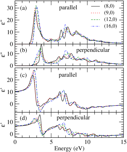
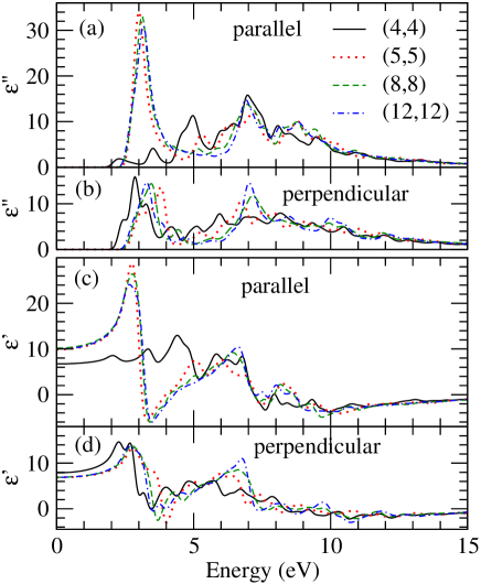
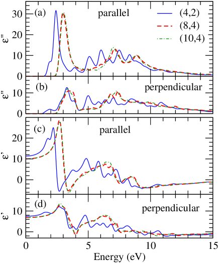
The calculated optical dielectric functions of some selected zigzag , armchair , chiral SiC-NTs are shown in Figs. 5-7, respectively. The spectra can be roughly divided into two regions, namely, the low-energy one from 2 to 6 eV and the high-energy one from 6 to 15 eV. Below about 2 eV (the band gap region), the is zero and tends to a constant as the photon energy approaches zero. For the electric field parallel to the tube axis (), the for all the three types of the SiC-NTs with a moderate diameter (say, 9 Å) in the low-energy region consists of a single distinct peak at 3 eV plus a long shoulder of 2 eV on the higher photon energy side (Figs. 5-7). This is very similar to the case of BN-NTs found in Ref. Lin, . Nonetheless, the peak in the SiC-NTs (Figs. 5-7) is about twice as high as that in the BN-NTs Lin , because the BN-NTs have a band gap which is in general twice wide than that of the SiC-NTs. However, this is in strong contrast to the case of CNTs in which the distinct features have been found especially for the semiconducting chiral nanotubes Chu and these features can be used to characterize the chirality of the grown carbon nanotubes by optical means li01 ; bac02 . Nevertheless, for small diameter SiC nanotubes, the spectrum can deviate markedly from the general behavior described above (see Figs. 5-7). For example, for the armchair (4,4) nanotube, the pronounced peak at 3 eV in the spectrum mentioned above is absent (Fig. 6a). For the chiral (4,2) nanotube, the pronounced peak in the spectrum shifts to low energy side by about 0.6 eV (Fig. 7a). In the high-energy region, the for all the types of the SiC-NTs have a broad peak of 6 eV wide centered at 8 eV.
For the electric field perpendicular to the tube axis (), the spectrum of all the SiC-NTs except the small diameter nanotubes such as the (8,0) and (4,4), in the low energy region also consists of a pronounced peak at around 3.5 eV whilst in the high-energy region is, roughly, made up of a broad hump starting from 6.0 eV (Figs. 5-7). The magnitude of the peaks is in general about half of the magnitude of the corresponding ones for , showing a moderate optical anisotropy in the SiC-NTs. In nanotubes, the electric field perpendicular to the nanotube axis is generally strongly screened aji94 ; Benedict ; mar03 ; koz06 ; guo07 , and this is known as the depolarization effect which is not taken into account in the present calculations. The depolarization effect may substantially reduce the magnitude of the spectrum for mar04 , and hence enhance the optical anisotropy.
Let us now compare the optical dielectric function of the SiC-NTs with that of the single SiC sheet. It is clear from Fig. 1 and Figs. 5-7 that the spectrum for of the SiC-NTs is very similar to that of the single SiC sheet for . This is particularly true for the large or even moderate diameter SiC-NTs in which the curvature effect is small. This is perhaps not surprising because the electric field polarization is parallel to the SiC layer in both cases. However, the spectrum for is rather different from that of of the single SiC sheet. In particular, the spectrum for for the photon energy below 5 eV is zero in the single SiC sheet (Fig. 1), whilst in contrast, the spectrum for of the SiC-NTs has a pronounced peak at 3.5 eV (Figs. 5-7). This perhaps can be explained as follows. When , it is clear that for some parts of the tube wall, the electric field is nearly perpendicular to the SiC layer whilst for the other parts of the tube wall, it is roughly parallel to the SiC layer. Therefore, the dielectric function for may be regarded as a mixture of the dielectric functions for both and of single SiC sheet. This can be seen from inspection of Fig. 1 and Figs. 5-7, and is especially clear for the large diameter SiC-NTs. As a result, the calculated optical anisotropy of the large SiC-NTs is smaller than that of the single SiC sheet. Nevertheless, as mentioned before, the depolarization effect for in the SiC-NTs may considerably enhance the optical anisotropy of especially small diameter SiC-NTs. Therefore, in optical experiments, one may still see a rather strong optical anisotropy because the spectrum for would be substantially reduced due to the depolarization effect.
III.4 Static dielectric response of the SiC nanotubes
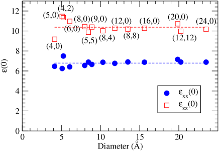
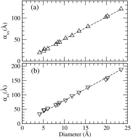
The optical dielectric function and electric polarizability in the zero frequency limit of the SiC-NTs are listed in Table III, and also displayed in Figs. 8 and 9. Note that the [] is the electronic contribution only [i.e., ()], and hence not the full static dielectric response [i.e., ()] which also contains the ionic contribution. In Ref. guo07, , it was found that including the ionic contribution would not change the observed trends, though the magnitude of the ionic contribution may be considerable.
Fig. 8 shows that to a first order approximation, the static dielectric constant is almost a constant (i.e., independent of the diameter). The average value of is 10.38 and 6.79 for and , respectively. The former is very close to of the single SiC sheet, while the latter is close to the circular average of the response of each part of the SiC-NT surface, which may be approximated by 0.5(+) with quantities for the single SiC sheet (see Table III). Note that the static dielectric constants of the SiC-NTs are about two times larger than that of the BN-NTs (4.6 for and 3.6 for ) Lin . Therefore, the SiC-NTs may be better dielectric materials than the BN-NTs. It is clear from Fig. 8 that there is a pronounced anisotropy in the static dielectric response of the SiC-NTs. Interestingly, there is a small but discernable chirality dependent oscillation centered at the average value of for both electric field polarizations. In particular, for , the zigzag SiC-NTs have a slightly larger dielectric constant than the armchair ones.
The electric polarizability per unit length for both and is proportional to the tube diameter , as shown in Fig. 9. By fitting a linear function = to the calculated -vs- curves, we obtain a slope = 5.20 for , and a slope = 7.81 for . As pointed out before for the BN-NTs Lin , this linear relation between and arises because the SiC-NTs are insulators in which the valence electrons are tightly bound to the ions and consequently, every atom of the same species has nearly the same static polarizability. Therefore, is proportional to the number of atoms per unit length which in turn is proportional to . Nevertheless, the SiC-NTs exhibit a much stronger dielectric response than the BN-NTs since the BN-NTs have significantly smaller slopes ( = 2.15, = 3.04). Lin This is because the SiC-NTs have a smaller band gap than the corresponding BN-NTs, as mentioned before.
Both the static dielectric constant and electric polarizability are clearly anisotropic. The anisotropy in electric polarizability can be best seen from the difference in the slopes between and , mentioned above. The for is about 50 % larger than that for . The actual anisotropy may be even larger because of the calculated and for would be reduced when the depolarization effect were taken into account.Benedict ; koz06 ; guo07
III.5 Electron energy loss spectrum
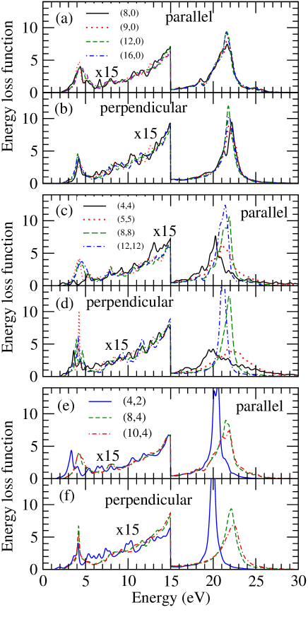
The calculated electron energy loss spectra of the zigzag, armchair and chiral SiC nanotubes are shown in Fig. 10. First of all, in the low energy region up to 15 eV, the EELS spectra for the all selected SiC nanotubes for both and [except (4,4) tube for ] (Fig. 10), look very similar to that of of the SiC sheet (Fig. 1e). In particular, all the spectra have a rather pronounced plasmon peak at 5 eV and then the spectra grow steadily with energy. In the high energy region from 15 eV upwards, the spectra are dominated by a large broad + plasmon peak with the exact peak positon being dependent on the chirality and also the electric field polarization. For the zigzag nanotubes, the energy position of the + plasmon peak is at 22 eV for both electric field polarizations. For the chiral (4,2) and (8,4) nanotubes, respectively, the plasmon peak occurs at 20 and 22 eV for both . For the armchair SiC nanotubes, the energy position of the + plasmon peak appears to oscillate around 21.5 eV (Fig. 10 c and d).
Surprisingly, there is only weak anisotropy in the EELS spectra for all the nanotubes (Fig. 10), in contrast to the rather pronounced anisotropy found in the dielectric functions (Figs. 5-7). The weak anisotropy in the EELS of the nanotubes may be attributed to the fact that for all the , , , and optical transitions are excited whilst the single SiC sheet only and transitions are possible for .
IV Summary
An ab initio study of the structural, electronic and optical properties of the SiC-NTs within density functioanal theory in the local density approximation has been performed. In particular, the properties of the single walled zigzag (3,0),(4,0),(5,0),(6,0),(8,0),(9,0),(12,0),(16,0),(20,0),(24,0), armchair (3,3),(4,4),(5,5),(8,8),(12,12),(15,15), and chiral nanotubes have been calculated. For comparison, the electronic structure and optical properties of the single SiC sheet have also been calculated. We find that all the SiC nanotubes are semiconductors with exceptions of the ultrasmall (3,0) and (4,0) zigzag tubes which may be regarded as the thinnest conducting SiC nanowires. Interestingly, the energy band gap of the zigzag SiC-NTs may be reduced from the full energy gap of the SiC sheet all the way down to zero by reducing the diameter (Fig. 2), though the band gap for all the SiC nanotubes with a diameter larger than 20 Å approaches that of the SiC sheet. Furthermore, all the semiconducting zigzag SiC-NTs have a direct band gap. All these suggest that they may have interesting applications in optical and optoelectronic devices. Nonetheless, both the armchair and chiral SiC-NTs have an indirect band gap.
The optical properties of the SiC-NTs, as for the SiC sheet, can be divided into two spectral regions, namely, the lower energy region (06 eV), in which the optical transitions involve mainly the -bands, and the higher energy region from 6 eV upwards, where interband transitions involve mainly the -bands. For , the for all the three types of the SiC-NTs with a moderate diameter (say, 8 Å for the zigzag SiC-NTs, 6 Å for the chiral SiC-NTs) in the low-energy region consists of a single distinct peak at 3 eV. However, for the small diameter SiC nanotubes such as the (4,2),(4,4) SiC-NTs, the spectrum does deviate markedly from this general behavior. In the high-energy region, the for all the SiC-NTs exhibit a broad peak centered near 7 eV. For , the spectrum of all the SiC-NTs except the (4,4), (3,0) and (4,0) nanotubes, in the low energy region also consists of a pronounced peak at around 3 eV whilst in the high-energy region is roughly made up of a broad hump starting from 6 eV. The magnitude of the peaks is in general about half of the magnitude of the corresponding ones for , showing a moderate optical anisotropy in the SiC-NTs.
Interestingly, unlike the CNTs, the calculated static dielectric constant for all the SiC nanotubes is almost independent of diameter and chirality with for being only about 30 % larger than for . This is very similar to the case of the BN-NTs except that the values of for the SiC nanotubes are about two times larger than that of the BN-NTs. The calculated electron energy loss spectra of all the SiC nanotubes studied here for both electric field polarizations are rather similar to that of of the SiC sheet, being dominated by a broad -electron plasmon peak at 21 eV and a small -electron plasmon peak at 3 eV.
V Acknowledgments
The authors gratefully acknowledge financial supports from National Science Council, Ministry of Economic Affairs (92-EC-17-A-08-S1-0006) and NCTS of ROC. They also thank National Center for High-performance Computing of ROC for providing CPU time.
References
- (1) S. Iijima, Nature (London) 354, 56 (1991).
- (2) R. Saito, G. Dresselhaus, and M. S. Dresselhaus, Physical properties of Carbon Nanotubes(Imperial College, London, 1998).
- (3) G. Y. Guo, K. C. Chu, D. S. Wang, and C. G. Duan, Phys.Rev. B 69, 205416 (2004).
- (4) G. Y. Guo, K. C. Chu, D. S. Wang, and C. G. Duan, Comput. Matter. Sci. 30, 269 (2004).
- (5) G. Y. Guo, J. C. Lin, Phys. Rev. B 71, 165402 (2005).
- (6) A. Rubio, J. L. Corkill, and M. L. Cohen, Phys. Rev. B 49, 5801 (1994).
- (7) M. Zhao, Y. Y. Xia, D. J. Zhang and L. M. Mei, Phys. Rev. B 68, 235415 (2003).
- (8) S. M. Lee, Y. H. Lee, Y. G. Hwang, J. Elsner, D. Porezag, and Th. Frauenheim, Phys. Rev. B 60, 7788 (1999).
- (9) von Münch, in Landolt-Börnstein, edited by O. Madelung, M. Schulz, and H. Weiss, New Series, Groups IV and III-V, Vol. 17, Pt. A (Springer, Berlin, 1982).
- (10) R. W. G. Wyckoff, Crystal Structures (Wiley, New York, 1963).
- (11) P. A. Ivanov and V. E. Chelnokov, Semicond. Sci. Technol. bf 7, 863 (1992).
- (12) C. Persson and U. Lindefelt, J. App. Phys. 82, 5496, (1997)
- (13) R. Wang, D. Zhang, C. Liu, Chemical Phys. Lett. 411, 333, (2005).
- (14) R. Rurali, P. Godigonon, J. Rebollo, E. Hernandez, and P. Ordejon, Appl. Phys. Lett. 82, 4298 (2003).
- (15) C. H. Park, B. H. Cheong, K. H. Lee, and K.J. Chang, Phys. Rev. B 49, 4485, (1994)
- (16) Properties of Silicon Carbide edited by G. L. Harris (INSPEC, Institution of Electrical Engineers, London,1995)
- (17) X.-H. Sun, C.-P. Li, W.-K. Wong, N.-B. Wong, C.-S. Lee, S.-T. Lee, and B.-K. Teo, J. Am. Chem. Soc. 124, 14464 (2002).
- (18) L. Z. Pei, Y. H. Tang, Y. W. Chen, C. Guo, X. X. Li, Y. Yuan, and Y. Zhang, J. Appl. Phys. 99, 114306 (2006).
- (19) L. Z. Pei,Y. H. Tang, X. Q.Zhao, Y. W. Chen and C. Guo, J. App. Phys. 100, 046105 (2006).
- (20) M. Menon, E. Richter, A. Mavrandonakis, G. Froudakis, and A. N. Andriotis, Phys. Rev. B 69, 115322 (2004).
- (21) M. Zhao, Y. Xia, F. Li, R. Q. Zhang and S. T. Lee, Phys.Rev. B 71, 085312 (2005).
- (22) A. Mavrandonakis, G. E. Froudakis, M. Schnell, and Muhlhauser, Nano Lett. 3, 1481 (2004).
- (23) Y. Miyamoto and B. D. Yu, Appl. Phys. Lett. 80, 586 (2002).
- (24) M. Zhao, Y. Xia, R. Q. Zhang, and S. T. Lee, J. Chem. Phys. 122, 214707 (2005).
- (25) A. Gali, Phys. Rev. B 73, 245415 (2006).
- (26) P. E. Blöchl, Phys. Rev. B 50, 17953 (1994); G. Kresse and D. Joubert, ibid. 59, 1758 (1999).
- (27) G. Kresse and J. Hafner, Phys. Rev. B 47, R558 (1993); 49, 14251 (1994); G. Kresse and J. Furthmüller, Comput. Mater. Sci. 6, 15 (1996).
- (28) B. Adolph, J. Furthmüller, and F. Bechstedt, Phys. Rev. B 63, 125108 (2001).
- (29) S. Okada, S. Saito, and A. Oshiyama, Phys. Rev. B 65, 165410 (2002).
- (30) X. Blase, A. Rubio, S. G. Louie, and M. L. Cohen, Europhys. Lett. 28, 335 (1994).
- (31) S.M. Bachilo, M.S. Strano, C. Kittrell, R.H. Hauge, R.E. Smalley, and R.B. Wiesman, Science 298, 2361 (2002).
- (32) Z.M. Li, Z.K. Tang, H.J. Liu, N. Wang, C.T. Chan, R. Saito, S. Okada, G.D. Li, J.S. Chen, N. Nagasawa and S. Tsuda, Phys. Rev. Lett. 87, 127401 (2001).
- (33) H. Ajiki and T. Ando, Physica B 201, 349 (1994); Jpn. J. Appl. Phys., Suppl. 34, 107 (1995).
- (34) L. X. Benedict, S. G. Louie, and M. L. Cohen, Phys. Rev. B 52, 8541 (1994).
- (35) A.G. Marinopoulos, L. Reining, A. Rubio, and N. Vast, Phys. Rev. Lett. 91, 46402 (2003).
- (36) B. Kozinsky and N. Marzari, Phys. Rev. Lett. 96, 166801 (2006).
- (37) G. Y. Guo, S. Ishibashi, T. Tamura and K. Terakura, Phys. Rev. B 75, 245403 (2007).
- (38) A. G. Marinopoulos, L. Wirtz, A. Marini, V. Olevano, A. Rubio, and L. Reining, Appl. Phys. A 78, 1157 (2004).
