Noise enhancement due to quantum coherence in coupled quantum dots
Abstract
We show that the intriguing observation of noise enhancement in the charge transport through two vertically coupled quantum dots can be explained by the interplay of quantum coherence and strong Coulomb blockade. We demonstrate that this novel mechanism for super-Poissonian charge transfer is very sensitive to decoherence caused by electron-phonon scattering as inferred from the measured temperature dependence.
pacs:
72.70.+m,73.23.-b,73.63.Kv,74.40.+kThe direct manifestation of quantum coherence in time-averaged transport observables of nanoscale conductors such as current or low-frequency current fluctuations is of great benefit since it allows for the study of decoherence in a straightforward manner. Quantum dots (QDs) coupled in series provide a perfect system to explore such effects since the quantum superposition of states in different dots has an immediate influence on the charge transfer van der Wiel et al. (2003). The effect of quantum coherence has been experimentally addressed mostly with respect to the average or time-dependent currents (e.g in Ref. Hayashi et al. (2003)), whereas until now current fluctuations as a very sensitive diagnostic tool Blanter and Büttiker (2000); Aguado and Brandes (2004); Fujisawa et al. (2006a) have not been investigated for this purpose.
In this Letter we demonstrate that our recent low-frequency shot noise data provide such a tool and are in fact a direct indicator of quantum coherent coupling between two layers of self-assembled InAs QDs Barthold et al. (2006). In our device, QD stacks are formed such that vertical tunneling through three barriers becomes possible. The corresponding current vs. applied bias voltage exhibits sharp peaks caused by the alignment of levels in a single QD stack. At the edges of these resonances the noise is enhanced above the Poissonian value for uncorrelated electron transfer ( is the unit charge and is the average current).
We find a striking agreement between our data and our calculations of this novel mechanism based on a quantum master equation for super-Poissonian charge transport in a single QD stack, which shows that contrary to the common view capacitive coupling between the stacks is not needed to explain the observed features. Typically, such noise behavior is associated with electron bunching in the charge transfer and has therefore received remarkable interest in recent experimental Iannaccone et al. (1998); Kuznetsov et al. (1998); Safonov et al. (2003); Gustavsson et al. (2006); Zarchin et al. (2007) and theoretical work Kießlich et al. (2003); Thielmann et al. (2005); Cottet et al. (2004); Belzig (2005); Djuric et al. (2005); Aghassi et al. (2006b). We also show that the decoherence due to electron-phonon scattering causes a temperature dependence that agrees with the measurements, allowing us to clearly identify the crossover between coherent and sequential tunneling.
Experiment. Here we summarize the features of the device and the experimental data Barthold et al. (2006) which are relevant for the subsequent theoretical discussion. The InAs quantum dot stacks are prepared by Stranski-Krastanov growth on AlAs and are sandwiched between three AlAs tunneling barriers. The three-dimensional electron reservoirs on both sides are formed in graded doped GaAs. The pyramid-shaped quantum dots partially penetrate the middle and top barrier which results in asymmetric tunneling rates.
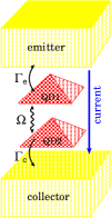
A sketch of the device geometry is shown in Fig. 1 (left). For the considered direction of the current – from top to bottom in Fig. 1 – the emitter barrier is effectively thinner, . The leverage factors for the quantum dots QD1 and QD2, i.e. the ratios of the potential drop between emitter and dot to the applied voltage , are estimated from the device geometry: and , respectively. The Fermi energy in the reservoir can be determined from a comparison with magneto-tunneling experiments for devices with only one layer of quantum dots. For devices with an otherwise identical growth scheme one finds an emitter Fermi level meV Hapke-Wurst et al. (2000).
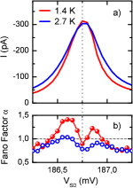
Due to the small size of the InAs quantum dots on AlAs the ground state energies and both lie above the Fermi energy and no current can flow through the device for . Due to the growth condition we also find that the top quantum dot QD1 is larger than the bottom one, . By applying a finite voltage the energy levels of the dots are shifted downwards by and brought into resonance. For we observe a peak in the tunneling current (Fig. 1a) van der Vaart et al. (1995). With increasing temperature the resonance broadens while the maximum remains nearly constant. Also a slight asymmetry with respect to the maximum can be observed. Both facts provide some indication for electron-phonon scattering in the tunneling process Fujisawa et al. (1998); Brandes and Kramer (1999) which will be discussed below in more detail.
The noise properties of the current in the range of the resonant tunneling peak is shown in Fig. 1b. The Fano factor vs. bias voltage displays an asymmetric double-peak structure with the maxima at the edges of the current resonance and values larger than unity indicating super-Poissonian noise. The noise is more sensitive to the temperature than the current: for larger temperatures the Fano factor peaks become smaller, and the super-Poissonian behavior vanishes. Far from the resonance we observe a noise suppression below the Poissonian value which we assume is due to some background current signal originated from leackage channels. In an ideal device the off-resonance electron transfer is Poissonian.
Model. We consider the coupled QD system as sketched in Fig. 1 (left) in the strong Coulomb blockade regime, i.e. only the occupation by a single excess electron is allowed. This restricts the dimension of the Hilbert space of the dot system spanned by the basis states for no excess electrons, for one excess electron in QD1 , and for one excess electron in QD2. The corresponding Hamiltonian can be written as
| (1) |
with the detuning of the QD levels which corresponds to an applied bias voltage, the tunnel coupling between the dots (see Fig. 1), , and . The second part in (1) describes the electron-phonon coupling and the phonon bath where is the creation operator of a phonon mode Q with frequency and is the coupling constant of electrons to phonon mode Q (for more details see Ref. Brandes and Vorrath (2002)). This spin-boson Hamiltonian will be coupled to the external electron reservoirs of emitter and collector contact. The quantum master equation for the reduced density matrix is then obtained from the von-Neumann equation for the total density matrix in Born-Markov approximation for weak contact coupling Elattari and Gurvitz (2002) and second-order perturbation theory in the electron-phonon coupling Brandes and Vorrath (2002):
| (7) |
with the reduced density matrix in vector form and the rates for coupling to the emitter/collector contact , respectively (see Fig. 1 left). The counting field which will be needed to calculate the current and the noise (see below) enters the matrix element in (7), where an electron jumps into the collector Kießlich et al. (2006).
The rates for the electron-phonon interaction in Eq. (7) are Brandes and Vorrath (2002); Brandes (2005)
with a dimensionless coupling constant , a high-frequency cutoff being an effective Debye frequency, and . These rates were derived for a bosonic environment with Ohmic spectral density which corresponds to bulk piezoelectric phonons in the limit and vanishing longitudinal speed of sound. Here and in the following we neglect the imaginary parts of .
The average current and the noise is computed with help of the cumulant generating function . It is defined by
| (9) |
with the distribution function of the number of transferred charges in the time interval . We obtain as the eigenvalue of the transition matrix in Eq. (7) which approaches zero for Kießlich et al. (2006). From the cumulant generating function the cumulants are obtained. Then, the average current is , the zero-frequency noise is , and the Fano factor reads . It is smaller than unity for sub-Poissonian and larger than unity for super-Poissonian charge transfer.
Discussion. Without electron-phonon interaction () we reproduce the known results for the current Stoof and Nazarov (1996); Gurvitz and Prager (1996)
| (10) |
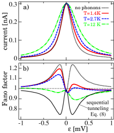
which provides a Lorentzian with respect to the detuning (bias voltage) as shown by the dotted curve in Fig. 2a and the Fano factor Elattari and Gurvitz (2002); Brandes (2005)
| (11) |
By close inspection of the Fano factor expression (11), super-Poissonian charge transfer occurs when the second term becomes negative. This occurs for and . In this case, the Coulomb interaction is more effective due to the smaller collector coupling, and two Fano factor peaks larger than unity and symmetric with respect to the current maximum appear (see dotted curve in Fig. 2b). We emphasize that this super-Poissonian transport behavior is only obtained for (i) coherent coupling between the dots and for (ii) strong Coulomb blockade. In order to verify this, we address these two issues in more detail.
(i) Consider a sequential tunneling approach, i.e. without non-diagonal elements of the density matrix: The master equation in strong Coulomb blockade for the diagonal elements of the density matrix reads
| (15) |
where is Fermi’s golden rule transition rate between states and Sprekeler et al. (2004). Note that due to the Coulomb blockade only the collector coupling enters this rate. Current and noise are computed by means of the cumulant generating function (9). Then this approach yields the same expression for the current (10) as the coherent description. The Fano factor is
| (16) |
Clearly, the sequential (incoherent) charge transfer turns out to be solely sub-Poissonian since the second term in (16) is always positive.
(ii) In order to relax the constraint of strong Coulomb blockade we extend the Hilbert space by the basis state for two excess electrons in the system. This leads to the master equation for the density matrix :
| (23) |
with . Here, for the sake of clarity we neglect the electron-phonon scattering. The resulting Fano factor also indicates overall sub-Poissonian transport behavior as we have checked numerically. Furthermore we can exclude double occupation of one of the dots since it has a rather low probability due to the large on site Coulomb energy in InAs QDs ( meV).
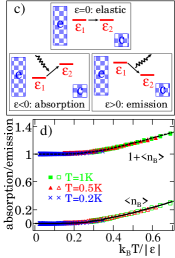
We will now discuss the influence of the finite temperature: With we can assume and for the Fermi functions of the leads for a typical situation as sketched in Fig. 2c. Therefore temperature acts solely due to the coupling to the phonon bath.
With electron-phonon interaction the calculated current and Fano factor vs. level detuning are shown in Fig. 2 a) and b) for three different temperatures. With increasing temperature the current resonance becomes asymmetrically broadened, whereas the maximum is not affected. For phonon absorption and for phonon emission take place, see Fig. 2c. From the data for the computed current we extract the corresponding phonon absorption and emission rates normalized by the rate for spontaneous phonon emission : for and for , respectively. According to the Einstein relations they should equal the Bose-Einstein distribution for absorption and for emission. In Fig. 2d we compare them as a function of Fujisawa et al. (1998).
The double peaks in the Fano factor discussed above, which were symmetric without coupling to the phonon bath (dotted curve in Fig. 2b), now become asymmetric with lower values above the resonance. For higher temperatures the Fano factor peaks decrease. This is in complete agreement with our experimental data (Fig. 1). This demonstrates that in the experiment, the transport of electrons through the dot system can be assumed to be partially coherent, strongly indicating electron-phonon scattering as the dephasing mechanism.
Furthermore, the low-frequency noise behavior enables the clear identification of a sequential and a coherent tunneling regime. In contrast to small temperatures, for higher 12 K (dash-dotted curve in Fig. 2b) the Fano factor indicates sub-Poissonian electron transfer for all bias voltages. Moreover, the Fano factor peaks at the edges of the resonance in the coherent tunneling regime turn into minima. Such behavior is also found by our Fano factor expression for sequential tunneling (16). A corresponding curve is shown in Fig. 2b clearly revealing the double minimum feature. Hence a double peak in the Fano factor refers to a coherent tunneling regime, whereas a double minimum indicates a sequential tunneling regime.
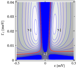
The crossover between these two regimes or between sub- and super-Poissonian charge transfer can also be induced by varying the collector coupling for fixed couplings , and temperature as shown in Fig. 3. The two different transport regimes are clearly distinguished: For small coupling ( 5eV) the sequential tunneling regime is recognized by the double minima with suppressed noise. For increasing a Fano factor larger than unity for indicates positive correlations in the charge transfer and consequently refers to coherent tunneling. Here the increased leads to shorter dwell time of the electrons on the dot and thus a smaller probability of a phonon absorbtion as the bath temperature is kept constant. If we increase above we find again a Fano factor smaller than unity. Therefore the super-Poissonian behavior is most pronounced with a maximum Fano factor for a certain collector coupling.
Conclusions. We have demonstrated that electron shot noise measurements provide a tool to detect the coherent coupling between quantum dots. We have compared low-frequency noise data with calculations based on quantum master equations which clearly demonstrate that the observed enhancement of the low-frequency noise at low temperatures is caused by the combined effect of strong Coulomb blockade and the quantum coherent transfer of electrons between the dots. We have furthermore shown that electron-phonon scattering as a source of decoherence is responsible for the experimental temperature dependence of current and noise.
Acknowledgements.
We acknowledge helpful discussions with Alessandro Braggio. This work was supported by Deutsche Forschungsgemeinschaft in the framework of Sfb 296, project BR/1528/5-1/, the WE-Heraeus foundation and the BMBF, project nanoQuit.References
- (1)
- van der Wiel et al. (2003) W. G. van der Wiel et al., Rev. Mod. Phys. 75, 1 (2003).
- Hayashi et al. (2003) T. Hayashi et al., Phys. Rev. Lett. 91, 226804 (2003).
- Blanter and Büttiker (2000) Y. M. Blanter and M. Büttiker, Phys. Rep. 336, 1 (2000).
- Aguado and Brandes (2004) R. Aguado and T. Brandes, Phys. Rev. Lett. 92, 206601 (2004).
- Fujisawa et al. (2006a) T. Fujisawa, et al., Science 312, 1634 (2006a).
- Barthold et al. (2006) P. Barthold et al., Phys. Rev. Lett. 96, 246804 (2006).
- Iannaccone et al. (1998) G. Iannaccone et al., Phys. Rev. Lett. 80, 1054 (1998).
- Kuznetsov et al. (1998) V. V. Kuznetsov et al., Phys. Rev. B 58, R10159 (1998).
- Safonov et al. (2003) S. S. Safonov et al., Phys. Rev. Lett. 91, 136801 (2003).
- Gustavsson et al. (2006) S. Gustavsson et al., Phys. Rev. B 74, 195305 (2006).
- Zarchin et al. (2007) O. Zarchin, et al., Phys. Rev. Lett. 98, 066801 (2007).
- Kießlich et al. (2003) G. Kießlich, A. Wacker, and E. Schöll, Phys. Rev. B 68, 125320 (2003).
- Thielmann et al. (2005) A. Thielmann et al., Phys. Rev. B 71, 045341 (2005).
- Cottet et al. (2004) A. Cottet, W. Belzig, and C. Bruder, Phys. Rev. B 70, 115315 (2004).
- Belzig (2005) W. Belzig, Phys. Rev. B 71, 161301(R) (2005).
- Djuric et al. (2005) I. Djuric, B. Dong, and H. L. Cui, Appl. Phys. Lett. 87, 032105 (2005).
- Aghassi et al. (2006b) J. Aghassi, et al., Phys. Rev. B 73, 195323 (2006b).
- Hapke-Wurst et al. (2000) I. Hapke-Wurst et al., Phys. Rev. B 62, 12621 (2000).
- van der Vaart et al. (1995) N. van der Vaart et al., Phys. Rev. Lett. 74, 4702 (1995).
- Fujisawa et al. (1998) T. Fujisawa et al., Science 282, 932 (1998).
- Brandes and Kramer (1999) T. Brandes and B. Kramer, Phys. Rev. Lett. 83, 3021 (1999).
- Brandes and Vorrath (2002) T. Brandes and T. Vorrath, Phys. Rev. B 66, 075341 (2002).
- Elattari and Gurvitz (2002) B. Elattari and S. A. Gurvitz, Phys. Lett. A 292, 289 (2002).
- Kießlich et al. (2006) G. Kießlich et al., Phys. Rev. B 73, 033312 (2006).
- Brandes (2005) T. Brandes, Phys. Rep. 408, 315 (2005).
- Stoof and Nazarov (1996) T. H. Stoof and Y. V. Nazarov, Phys. Rev. B 53, 1050 (1996).
- Gurvitz and Prager (1996) S. A. Gurvitz and Y. S. Prager, Phys. Rev. B 53, 15932 (1996).
- Sprekeler et al. (2004) H. Sprekeler et al., Phys. Rev. B 69, 125328 (2004).